EP1071005A2 - Data transfer apparatus for system having plural clock domains - Google Patents
Data transfer apparatus for system having plural clock domains Download PDFInfo
- Publication number
- EP1071005A2 EP1071005A2 EP00114590A EP00114590A EP1071005A2 EP 1071005 A2 EP1071005 A2 EP 1071005A2 EP 00114590 A EP00114590 A EP 00114590A EP 00114590 A EP00114590 A EP 00114590A EP 1071005 A2 EP1071005 A2 EP 1071005A2
- Authority
- EP
- European Patent Office
- Prior art keywords
- clock
- data
- latch
- clocked
- domain
- Prior art date
- Legal status (The legal status is an assumption and is not a legal conclusion. Google has not performed a legal analysis and makes no representation as to the accuracy of the status listed.)
- Ceased
Links
Images



Classifications
-
- H—ELECTRICITY
- H04—ELECTRIC COMMUNICATION TECHNIQUE
- H04L—TRANSMISSION OF DIGITAL INFORMATION, e.g. TELEGRAPHIC COMMUNICATION
- H04L7/00—Arrangements for synchronising receiver with transmitter
-
- G—PHYSICS
- G06—COMPUTING OR CALCULATING; COUNTING
- G06F—ELECTRIC DIGITAL DATA PROCESSING
- G06F5/00—Methods or arrangements for data conversion without changing the order or content of the data handled
- G06F5/06—Methods or arrangements for data conversion without changing the order or content of the data handled for changing the speed of data flow, i.e. speed regularising or timing, e.g. delay lines, FIFO buffers; over- or underrun control therefor
-
- H—ELECTRICITY
- H04—ELECTRIC COMMUNICATION TECHNIQUE
- H04L—TRANSMISSION OF DIGITAL INFORMATION, e.g. TELEGRAPHIC COMMUNICATION
- H04L7/00—Arrangements for synchronising receiver with transmitter
- H04L7/0008—Synchronisation information channels, e.g. clock distribution lines
- H04L7/0012—Synchronisation information channels, e.g. clock distribution lines by comparing receiver clock with transmitter clock
-
- H—ELECTRICITY
- H04—ELECTRIC COMMUNICATION TECHNIQUE
- H04L—TRANSMISSION OF DIGITAL INFORMATION, e.g. TELEGRAPHIC COMMUNICATION
- H04L7/00—Arrangements for synchronising receiver with transmitter
- H04L7/0016—Arrangements for synchronising receiver with transmitter correction of synchronization errors
- H04L7/0045—Correction by a latch cascade
-
- H—ELECTRICITY
- H04—ELECTRIC COMMUNICATION TECHNIQUE
- H04L—TRANSMISSION OF DIGITAL INFORMATION, e.g. TELEGRAPHIC COMMUNICATION
- H04L7/00—Arrangements for synchronising receiver with transmitter
- H04L7/02—Speed or phase control by the received code signals, the signals containing no special synchronisation information
Definitions
- This invention relates to transferring data between systems having a plurality of clocks with a plurality of different frequencies.
- known systems utilize buffer memory and/or condition the phase of the clock in one or both of the clock domains to avoid the metastability.
- An example of this approach is described in United States Patent No. 5,548,620.
- data is clocked through a master and a slave flip-flop at the output of the first domain and a master and a slave flip-flop at the input of the second domain.
- the master flip-flop of the first domain is clocked by the first domain clock.
- the slave flip-flop in the second domain is clocked by the second domain clock.
- the slave flip-flop in the first domain and the master flip-flop in the second domain are both clocked by respectively different clocks that are generated in phase locked loop circuitry.
- the present invention is directed to clock domain interface circuitry for providing data interfacing between clock domains.
- This circuitry includes a first latch at the output of a first clock domain, and a second latch at the input to the second clock domain.
- the first and second latches are clocked by their respective domain clocks.
- An Enable Signal which is a logical function of the respective clocks is applied to enable one of the first and second latches.
- Figure 1 is an interface integrated circuit which is useful in defining an environment of the invention, but is not restrictive.
- the invention may be practiced in any integrated circuit (IC) or other closely packed circuitry such as a multichip IC package or hybrid IC package incorporating multiple clock domains.
- IC integrated circuit
- Other examples may include multiprocessor IC's for multimedia processing, multichannel digital audio processing/editing IC's and systems, just to name a few.
- Figure 1 illustrates an interface or link IC for a multiplatform television system.
- This IC is configured to simultaneously digitally process a plurality of television signals received in different formats.
- the respective processors are circumscribed with dashed lines.
- the circuitry circumscribed with dashed line 10 is configured to process digital direct broadcast satellite signal.
- This circuitry includes two analog to digital converters for processing quadrature signals from a satellite tuner, a digital demodulator and error correction circuitry.
- the respective elements within this circuitry may require different clocking signals such as for example, 18 MHz, 54 MHz and 27 MHz clock signals and thus may include a plurality of clock domains.
- Various control signals from the microprocessor interface may be coupled to ones of these domains.
- a second processing block circumscribed by the dashed line 20 receives and processes high definition digital signals such as may be transmitted according to the Grand Alliance protocol.
- This circuitry includes at least one analog to digital converter, a digital demodulator, an equalizer/phase tracker and error correction circuitry. These elements may require different clocking signals such as, for example, 108 MHz, 54 MHz and 18 MHz clock signals, and thus includes another plurality of clock domains.
- the IC includes an NTSC signal processor circumscribed by the dashed line 31.
- This circuitry includes analog to digital converters, filter circuitry, and digital color decoders. . These elements may require different clocking signals such as, for example, 18 MHz, 36 MHz and 27 MHz clock signals, representing another plurality of clock domains.
- Each of the respective larger blocks of circuitry includes a plurality of clock domains. However it is unlikely that control data will be provided to circuitry in each of the clock domains. It is likely that control data from the microprocessor will be required from more than one domain and that control data will be transferred between different domains.
- the respective clocking signals will be provided by common clock generation circuitry including a phase locked loop 12 to develop a master clock signal and a generator 14 responsive to the master clock signal for providing a plurality of clock signals at different frequencies.
- the master clock is at 108 MHz
- the further clock signals are at 18, 27, 36 and 54 MHz.
- Figure 2 illustrates exemplary timing relationships of these clock signals. These particular clock signals are phase locked to each other and are all simple multiples of 9 MHz. It will be appreciated that a plurality of clock signals widely divergent from those illustrated may be employed in similar or different IC's, and to which the invention will apply.
- Timing margins may be determined by examination of the exemplary waveforms of Figure 2. In Figure 2, all of the clock signals have rising transitions at the points designated A.. Thus there is a zero timing margin between all domains and a high likelihood that a data error may occur if data is transferred at these instances.
- timing margin at point B between the 18 and 27 MHz clock domains.
- Figure 8 illustrates exemplary Enable Pulse timing where data transfer is to occur between 18 MHz, 27 MHz and 36 MHz clock domains. It will be recognized that, if the data is not synchronized to the Enable Pulses, each data word must be present for at least two cycles of the 18 MHz clock to insure data transfer. If a data word is lesser in duration it could occur between the Enable Signal pulses an be lost.
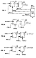
- Figures 3-6 illustrate respective circuits for transferring data between respective clock domains.
- Figure 3 illustrates circuitry for transferring data from a 27 MHz clock domain to a 18 MHz clock domain.
- the circuitry includes an Enabled Data Latch 30 and a simple Data Latch 32. Data is stored or latched into the respective latches coincident with positive going transitions of the respective clock signal.
- This Enabled Data Latch comprises a simple Data Latch 92 and a multiplexor 90
- the multiplexor is connected to feed back the output of the Data Latch 92 when the Enable Pulse is low and to input new data to the Data Latch 92 when the Enable Pulse is high.
- New data is loaded into the latch during positive transitions of the clock signal only when the Enable Signal is in a high logic state.
- the new data loaded into the Data Latch 92 is stored until the next coincidence of the Enable Pulse and a positive transition of the clock pulse.
- new data can be loaded into the Enabled Data Latch 30 at times designated 30T when the 27 MHz clock exhibits a positive transition and enable is high. This data will remain in Enabled Data Latch 30 until at least the next occurring time designated 30T.
- New data loaded in Enabled Data Latch 30, at the output of 27 MHz clock domain will be loaded into Data Latch 32, at the input of the 18MHz clock domain, during the next positive transition of the 18 MHz clock following time 30T. This transition is designated 32T in Figure 8. It will be recognized that there is a full half cycle of the 27 MHz clock timing margin for transfer between clock domains.
- Figure 4 illustrates circuitry for transferring data from a 27 MHz clock domain to a 36 MHz clock domain.
- the circuitry includes an Enabled Data Latch 40 and a simple Data Latch 42.
- Enabled Data Latch 40 is similar in design to Enabled Data Latch 30. Referring to Figure 8, new data can be loaded into the Enabled Data Latch 40 at times designated 30T when the 27 MHz clock exhibits a positive transition and the Enable Signal is high. This data will remain in the Enabled Data Latch 40 until at least the next occurring time designated 30T.
- New data loaded in the Enabled Data Latch 40, at the output of 27 MHz clock domain, will be loaded into Data Latch 42, at the input of the 36 MHz clock domain, during the next positive transition of the 36 MHz clock following time 30T. This occurs at time 32T in Figure 8.
- Figure 5 illustrates circuitry for transferring data from a 18 MHz clock domain to a 27 MHz clock domain.
- the circuitry includes a Data Latch 50 and an Enabled Data latch 52.
- Enabled Data Latch 52 is similar in design to Enabled Data Latch 30.
- new data can be loaded into the Data Latch 50 at all positive transition of the 18 MHz clock. This data will remain in Data Latch 50 until at least the next positive transition of the 18 MHz clock, but remember in this example, data word duration must be at least two cycles of the 18 MHz clock. Assume that new data is loaded in Data Latch 50, at the output of 18 MHz clock domain, at time 50T.
- This data will be loaded into Enabled Data Latch 52, at the input of the 27 MHz clock domain, during the next positive transition of the 27 MHz clock when the Enable Pulse is high. This occurs at time 30T in Figure 8.
- the timing margin for this transfer between clock domains is almost a full cycle of the 27 MHz clock.
- Figure 6 illustrates circuitry for transferring data from a 36 MHz clock domain to a 27 MHz clock domain.
- the circuitry includes a Data Latch 60 and an Enabled Data latch 62.
- Enabled Data Latch 62 is similar in design to Enabled Data Latch 30.
- new data can be loaded into the Data Latch 60 at all positive transition of the 36 MHz clock. This data will remain in Data Latch 60 until at least the next positive transition of the 36 MHz clock, but remember in this example, data word duration must be at least two cycles of the 18 MHz clock. Assume that new data is loaded in Data Latch 60, at the output of 36 MHz clock domain, at time 60T.
- This data will be loaded into Enabled Data Latch 62, at the input of the 27 MHz clock domain, during the next positive transition of the 27 MHz clock when the Enable Pulse is high. This occurs at time 30T in Figure 8.
- the timing margin for this transfer between clock domains is one full cycle of the 108 MHz clock.
- Figure 9 illustrates exemplary circuitry for generating the Enable Signal.
- the 18 MHz, 27 MHz, 36 MHz and 54 MHz clock signals are logically ANDED to generate a reset pulse occurring at time 50T.
- This reset pulse is applied to a counter 70, arranged to count pulses of the complement of the 108 MHz clock signal.
- Counter 70 provides a pulse which is 4 cycles of the 108 MHz clock in duration, and which begins with the negative going transition of the 108 MHz clock following the reset pulse; that is, one half cycle of the 108 MHz clock following time 50T.
- Figure 10 illustrates a second embodiment of an Enable Signal generator.
- Figure 11 shows the relevant waveforms output by respective elements in Figure 10.
- the 18 MHz clock is divided by two in circuit 102 to generate a squarewave (designated 18/2 in Figure 11) delayed one half cycle of the 108 MHz clock and having a cycle time equal to the duration of the enable cycle.
- the complement of this signal is logically ANDED (104) with the complement of the 108 MHz clock signal to provide a gated clock signal (GATED CK).
- the first pulse of the gated clock occurs one half cycle of the 108 MHz clock signal following time 50T.
- the gated clock is applied to a divide by 8 circuit 106.
- the output of the divide by 8 circuit goes high and continues high for the duration of the gated clock pulses.
- the 18/2 signal is applied to the reset input of the divide by 8 circuit 106, and causes the output of the divide by 8 circuit to be reset low coincident with the positive portion of the 18/2 signal.
- the complement of the 18/2 signal is logically ANDED with the complement of the signal from the divide by 8 circuit 106 in the AND circuit 108 to provide the Enable Signal.
- Figure 12 shows a third alternative Enable Signal generating circuit. This circuit is derived from simple logic manipulation of the available clock signals which those skilled in the art of logic design will readily understand.
- a generic graphical approach to generating the Enable Signal is to draw a timing diagram of the relevant clock signals with at least one complete cycle of the lowest common multiple of the clock periods included.
- the rising edges of each output domain clock is examined to determine if any rising edges of the input domain clocks are unacceptably close.
- the Enable Signal is drawn with a low logic level in all areas that the edges are unacceptably close and high otherwise. Thereafter it is generally possible to create an Enable Signal that is a superset (e.g. logical AND) of the various clock signals.
- a state machine may be programmed to generate it. Note, "unacceptably close" edges are determined by worst case jitter/phase variation analysis between input and output clocks, taking the physical location of the relevant interface circuits into consideration.
Landscapes
- Engineering & Computer Science (AREA)
- Computer Networks & Wireless Communication (AREA)
- Signal Processing (AREA)
- Theoretical Computer Science (AREA)
- Physics & Mathematics (AREA)
- General Engineering & Computer Science (AREA)
- General Physics & Mathematics (AREA)
- Synchronisation In Digital Transmission Systems (AREA)
Abstract
Description
| INPUT CLOCK MHz | OUTPUT CLOCK MHz | MARGIN AT A ns | MARGIN AT B ns | MARGIN AT |
| 27 | 18 | 0 | 18.5 | 37.0 |
| 27 | 36 | 0 | 18.5 | 9.3 |
| 18 | 27 | 0 | 37.0 | 18.5 |
| 36 | 27 | 0 | 9.3 | 18.5 |
Claims (8)
- Interface apparatus for interfacing data to a plurality of different clock domains where the clock signals in the different domains are phase locked together and respective clock signals have different frequencies, and the data rate of data to be interfaced is slower than the clock rate of the slowest domain clock, said interface apparatus characterized by:a plurality of cascade connected first and second latches (30,32; 40,42; 50,52; 60, 62) coupled between respective clock domains, one of said first and second latches being a clocked Data Latch (32; 42; 50; 60) and the other of said first and second latches being a clocked and Enabled Data Latch (30; 40; 52; 62), respective clocked Data Latchs having a data and a clock input connection and a data output connection, and respective clocked and Enabled Data Latches each having a clock and an enable input connections and a data output connection;a timing generator (14) having output connections providing respective domain clock signals, wherein a domain clock signal of a domain providing a data signal is applied to the clock input connection of the first latch of a respective cascade connected set of latches and a domain clock signal of a domain receiving said data signal is applied to the second latch of a respective cascade connected set of latches;said timing generator providing a common Enable Signal phase locked (12) to said domain clocked signals, said common Enable Signal being applied to the enable input signal of one of said first and second latches of each set of cascade connected set of latches.
- The interface apparatus set forth in claim 1 characterized in that respective clocked and Enabled Data Latches comprise:a clocked Data Latch having input, output and clock connections;a multiplexor having an output coupled to the input connection of said clocked Data Latch; a first input connection connected to the output connection of said clocked Data Latch, a second input connection for receiving data signal and a control input connected to said Enable Signal; and
wherein the output connection of the clocked Data Latch provides the output signal of the clocked and Enabled Data Latch, and the second input connection of the multiplexor is the input connection of the clocked and Enabled Data Latch. - The interface apparatus set forth in claim 1 arranged for interfacing data from a 27 MHz clock domain to a 36 MHz clock domain characterized in that in said first latch in said cascade connection is a clocked and Enabled Data Latch having its clock input connection connected to a 27 MHz clock signal, and said second latch of said cascade connection is a clocked Data Latch having its clock input connection connected to a 36 MHz clock signal.
- The interface apparatus set forth in claim 1 arranged for interfacing data from a 27 MHz clock domain to a 18 MHz clock domain characterized in that in said first latch in said cascade connection is a clocked and Enabled Data Latch having its clock input connection connected to a 27 MHz clock signal, and said second latch of said cascade connection is a clocked Data Latch having its clock input connection connected to a 18 MHz clock signal.
- The interface apparatus set forth in claim 1 arranged for interfacing data from a 18 MHz clock domain to a 27 MHz clock domain characterized in that in said first latch in said cascade connection is a clocked Data Latch having its clock input connection connected to a 18 MHz clock signal, and said second latch of said cascade connection is a clocked and Enabled Data Latch having its clock input connection connected to a 27 MHz clock signal.
- The interface apparatus set forth in claim 1 arranged for interfacing data from a 36 MHz clock domain to a 27 MHz clock domain characterized in that in said first latch in said cascade connection is a clocked Data Latch having its clock input connection connected to a 36 MHz clock signal, and said second latch of said cascade connection is a clocked and Enabled Data Latch having its clock input connection connected to a 27 MHz clock signal.
- The interface apparatus set forth in claim 6 further characterized by interface apparatus arranged for interfacing data from a 27 MHz clock domain to a 36 MHz clock domain wherein in said first latch in said cascade connection is a clocked and Enabled Data Latch having its clock input connection connected to a 27 MHz clock signal, and said second latch of said cascade connection is clocked Data Latch having its clock input connection connected to a 36 MHz clock signal.
- The interface apparatus set forth in claim 4 further characterized by a further interface apparatus having third and fourth cascade connected latches arranged for interfacing data from a 27 MHz clock domain to a 36 MHz clock domain wherein in said third latch in said cascade connection is a clocked and Enabled Data Latch having its clock input connection connected to a 27 MHz clock signal, and said fourth latch of said cascade connection is a clocked Data Latch having its clock input connection connected to a 36 MHz clock signal.
Applications Claiming Priority (2)
| Application Number | Priority Date | Filing Date | Title |
|---|---|---|---|
| US356820 | 1999-07-19 | ||
| US09/356,820 US6549593B1 (en) | 1999-07-19 | 1999-07-19 | Interface apparatus for interfacing data to a plurality of different clock domains |
Publications (2)
| Publication Number | Publication Date |
|---|---|
| EP1071005A2 true EP1071005A2 (en) | 2001-01-24 |
| EP1071005A3 EP1071005A3 (en) | 2003-06-25 |
Family
ID=23403091
Family Applications (1)
| Application Number | Title | Priority Date | Filing Date |
|---|---|---|---|
| EP00114590A Ceased EP1071005A3 (en) | 1999-07-19 | 2000-07-07 | Data transfer apparatus for system having plural clock domains |
Country Status (5)
| Country | Link |
|---|---|
| US (1) | US6549593B1 (en) |
| EP (1) | EP1071005A3 (en) |
| JP (1) | JP4663070B2 (en) |
| KR (1) | KR100711131B1 (en) |
| CN (1) | CN1201547C (en) |
Cited By (3)
| Publication number | Priority date | Publication date | Assignee | Title |
|---|---|---|---|---|
| WO2004059471A3 (en) * | 2002-12-19 | 2005-06-23 | Mosaid Technologies Inc | Clock skew compensation apparatus and method |
| EP1601131A1 (en) * | 2004-05-24 | 2005-11-30 | Stmicroelectronics, Ltd. | Asynchronous multi-clock system |
| WO2007041107A3 (en) * | 2005-10-03 | 2007-06-07 | Spansion Llc | Digital data transfer between different clock domains |
Families Citing this family (12)
| Publication number | Priority date | Publication date | Assignee | Title |
|---|---|---|---|---|
| US6910145B2 (en) * | 2001-12-13 | 2005-06-21 | Emc Corporation | Data transmission across asynchronous clock domains |
| GB0204144D0 (en) * | 2002-02-22 | 2002-04-10 | Koninkl Philips Electronics Nv | Transferring data between differently clocked busses |
| US6954869B2 (en) * | 2002-09-26 | 2005-10-11 | Analog Devices, Inc. | Methods and apparatus for clock domain conversion in digital processing systems |
| US6958953B2 (en) * | 2003-05-13 | 2005-10-25 | International Business Machines Corporation | Real time clock circuit having an internal clock generator |
| JP4457074B2 (en) * | 2003-11-20 | 2010-04-28 | 株式会社アドバンテスト | Timing comparator, data sampling device, and test device |
| WO2006030904A1 (en) * | 2004-09-16 | 2006-03-23 | Nec Corporation | Semiconductor device and communication control method |
| US7809972B2 (en) * | 2007-03-30 | 2010-10-05 | Arm Limited | Data processing apparatus and method for translating a signal between a first clock domain and a second clock domain |
| JP5431290B2 (en) * | 2010-10-29 | 2014-03-05 | インターナショナル・ビジネス・マシーンズ・コーポレーション | Clock domain crossing data transfer circuit and method |
| US20120198267A1 (en) | 2011-01-31 | 2012-08-02 | Srinjoy Das | System and Method for Facilitating Data Transfer Between a First Clock Domain and a Second Clock Domain |
| GB2503474B (en) * | 2012-06-27 | 2016-06-29 | Nordic Semiconductor Asa | Data transfer between clock domains |
| KR20230033785A (en) * | 2021-09-01 | 2023-03-09 | 삼성전자주식회사 | Error Correcting Circuit using multi-clock and Semiconductor device including the same |
| KR102551602B1 (en) * | 2021-11-02 | 2023-07-04 | 서울시립대학교 산학협력단 | High-speed decision feedback equalizer including a plurality of cascaded latches |
Family Cites Families (17)
| Publication number | Priority date | Publication date | Assignee | Title |
|---|---|---|---|---|
| JPS56140459A (en) | 1980-04-04 | 1981-11-02 | Hitachi Ltd | Data processing system |
| US4970676A (en) * | 1989-04-04 | 1990-11-13 | Rca Licensing Corporation | Digital word-serial multiplier circuitry |
| US5045801A (en) | 1990-05-29 | 1991-09-03 | The United States Of America As Represented By The Secretary Of The Air Force | Metastable tolerant asynchronous interface |
| JPH0556085A (en) | 1991-08-23 | 1993-03-05 | Nec Ic Microcomput Syst Ltd | Interface circuit |
| US5256912A (en) * | 1991-12-19 | 1993-10-26 | Sun Microsystems, Inc. | Synchronizer apparatus for system having at least two clock domains |
| US5392422A (en) | 1992-06-26 | 1995-02-21 | Sun Microsystems, Inc. | Source synchronized metastable free bus |
| US5357613A (en) * | 1992-09-16 | 1994-10-18 | Texas Instruments Incorporated | Time-domain boundary buffer method and apparatus |
| US5422914A (en) | 1993-09-07 | 1995-06-06 | Motorola, Inc. | System and method for synchronizing data communications between two devices operating at different clock frequencies |
| GB2282472B (en) | 1993-10-01 | 1998-07-15 | Nokia Mobile Phones Ltd | An interface between unsynchronised devices |
| JPH07200095A (en) * | 1993-12-28 | 1995-08-04 | Victor Co Of Japan Ltd | Data transfer circuit |
| US5548620A (en) | 1994-04-20 | 1996-08-20 | Sun Microsystems, Inc. | Zero latency synchronized method and apparatus for system having at least two clock domains |
| SG47976A1 (en) * | 1994-05-10 | 1998-04-17 | Intel Corp | Method and apparatus for providing synchronous data transmission between digital devices operating at frequencies having a p/q integer ratio relationship |
| US5510732A (en) | 1994-08-03 | 1996-04-23 | Sun Microsystems, Inc. | Synchronizer circuit and method for reducing the occurrence of metastability conditions in digital systems |
| US5598113A (en) | 1995-01-19 | 1997-01-28 | Intel Corporation | Fully asynchronous interface with programmable metastability settling time synchronizer |
| WO1997006491A1 (en) | 1995-08-10 | 1997-02-20 | International Business Machines Corporation | Synchronizing logic avoiding metastability |
| JPH09233483A (en) * | 1996-02-22 | 1997-09-05 | Sony Corp | Method and apparatus for transmitting digital color video signal |
| JP4130006B2 (en) * | 1998-04-28 | 2008-08-06 | 富士通株式会社 | Semiconductor device |
-
1999
- 1999-07-19 US US09/356,820 patent/US6549593B1/en not_active Expired - Lifetime
-
2000
- 2000-07-07 EP EP00114590A patent/EP1071005A3/en not_active Ceased
- 2000-07-13 KR KR1020000040230A patent/KR100711131B1/en not_active Expired - Fee Related
- 2000-07-18 JP JP2000218010A patent/JP4663070B2/en not_active Expired - Fee Related
- 2000-07-18 CN CNB00120145XA patent/CN1201547C/en not_active Expired - Fee Related
Cited By (12)
| Publication number | Priority date | Publication date | Assignee | Title |
|---|---|---|---|---|
| WO2004059471A3 (en) * | 2002-12-19 | 2005-06-23 | Mosaid Technologies Inc | Clock skew compensation apparatus and method |
| US7010713B2 (en) | 2002-12-19 | 2006-03-07 | Mosaid Technologies, Inc. | Synchronization circuit and method with transparent latches |
| JP2006511899A (en) * | 2002-12-19 | 2006-04-06 | モサイド・テクノロジーズ・インコーポレイテッド | Slave QDRII compliant coprocessor |
| US7596710B2 (en) | 2002-12-19 | 2009-09-29 | Mosaid Technologies Incorporated | Synchronization circuit and method with transparent latches |
| US8069363B2 (en) | 2002-12-19 | 2011-11-29 | Mosaid Technologies Incorporated | Double data rate output latch for static RAM device has edge-triggered flip-flop to output DDR signal to synchronize with a second clock signal |
| US8296598B2 (en) | 2002-12-19 | 2012-10-23 | Mosaid Technologies Incorporated | Double data rate output circuit and method |
| US8533522B2 (en) | 2002-12-19 | 2013-09-10 | Mosaid Technologies Incorporated | Double data rate output circuit |
| EP1601131A1 (en) * | 2004-05-24 | 2005-11-30 | Stmicroelectronics, Ltd. | Asynchronous multi-clock system |
| US7545896B2 (en) | 2004-05-24 | 2009-06-09 | Stmicroelectronics Limited | Asynchronous multi-clock system |
| US7929655B2 (en) | 2004-05-24 | 2011-04-19 | Stmicroelectronics Limited | Asynchronous multi-clock system |
| WO2007041107A3 (en) * | 2005-10-03 | 2007-06-07 | Spansion Llc | Digital data transfer between different clock domains |
| US7813459B2 (en) | 2005-10-03 | 2010-10-12 | Spansion Llc | Digital data transfer between different clock domains |
Also Published As
| Publication number | Publication date |
|---|---|
| JP4663070B2 (en) | 2011-03-30 |
| EP1071005A3 (en) | 2003-06-25 |
| KR20010049781A (en) | 2001-06-15 |
| CN1201547C (en) | 2005-05-11 |
| JP2001077797A (en) | 2001-03-23 |
| US6549593B1 (en) | 2003-04-15 |
| KR100711131B1 (en) | 2007-04-27 |
| CN1281306A (en) | 2001-01-24 |
Similar Documents
| Publication | Publication Date | Title |
|---|---|---|
| US6549593B1 (en) | Interface apparatus for interfacing data to a plurality of different clock domains | |
| US6247082B1 (en) | Method and circuit for providing handshaking to transact information across multiple clock domains | |
| US5274678A (en) | Clock switching apparatus and method for computer systems | |
| US4575644A (en) | Circuit for prevention of the metastable state in flip-flops | |
| JPH05289770A (en) | Method and device for synchronization | |
| GB2074819A (en) | Multi-source/receiver data processing system | |
| US5408641A (en) | Programmable data transfer timing | |
| US5357613A (en) | Time-domain boundary buffer method and apparatus | |
| JPH0784668A (en) | System and method for synchronization of data | |
| US5291529A (en) | Handshake synchronization system | |
| US6087867A (en) | Transaction control circuit for synchronizing transactions across asynchronous clock domains | |
| US6044121A (en) | Method and apparatus for recovery of time skewed data on a parallel bus | |
| CN114911743B (en) | SPI slave device, SPI master device and related communication method | |
| US5442658A (en) | Synchronization apparatus for a synchronous data processing system | |
| US6348828B1 (en) | Clock enable circuit for use in a high speed reprogrammable delay line incorporating glitchless enable/disable functionality | |
| JP3320469B2 (en) | Data processing circuit layout | |
| JPS59229779A (en) | Series-parallel-series type integrated memory circuit | |
| MXPA00007049A (en) | Data transfer apparatus for system having plural clock domains | |
| EP0520836A2 (en) | Apparatus for simultaneous write access to a single bit memory | |
| EP0285892A2 (en) | Clock skew compensation system for pipeline processors | |
| US4809302A (en) | Clock injector circuit | |
| US5023870A (en) | Interface circuit for data transmission between a microprocessor system and a time-division-multiplexed system | |
| JP3688137B2 (en) | Microcomputer | |
| US5530727A (en) | Half synchronizer circuit interface system | |
| US4975911A (en) | Interface circuit for data transmission between a microprocessor system and a time-division-multiplexed system |
Legal Events
| Date | Code | Title | Description |
|---|---|---|---|
| PUAI | Public reference made under article 153(3) epc to a published international application that has entered the european phase |
Free format text: ORIGINAL CODE: 0009012 |
|
| AK | Designated contracting states |
Kind code of ref document: A2 Designated state(s): AT BE CH CY DE DK ES FI FR GB GR IE IT LI LU MC NL PT SE |
|
| AX | Request for extension of the european patent |
Free format text: AL;LT;LV;MK;RO;SI |
|
| PUAL | Search report despatched |
Free format text: ORIGINAL CODE: 0009013 |
|
| AK | Designated contracting states |
Designated state(s): AT BE CH CY DE DK ES FI FR GB GR IE IT LI LU MC NL PT SE |
|
| AX | Request for extension of the european patent |
Extension state: AL LT LV MK RO SI |
|
| 17P | Request for examination filed |
Effective date: 20031213 |
|
| AKX | Designation fees paid |
Designated state(s): DE FR GB IT |
|
| 17Q | First examination report despatched |
Effective date: 20040319 |
|
| STAA | Information on the status of an ep patent application or granted ep patent |
Free format text: STATUS: THE APPLICATION HAS BEEN REFUSED |
|
| 18R | Application refused |
Effective date: 20041025 |