BACKGROUND OF THE INVENTION
The present invention relates to a communication
interface apparatus which is suitable for operation with
electric power received from a communication line.
A communication apparatus (called the "terminal")
adapted to operate with electric power received from
a communication line (called the "power reception") is
utilized for a telephone and a modem unit for use with a
telephone line. The electric power is supplied (called the
"powering") from a subscriber line interface located in an
end office (EO) (hereinafter simply called the "station")
For this reason, a terminal located far away from the
station is concerned with a lower received voltage due to
a loss through the subscriber line, thereby making the
terminal inoperative. As a terminal circuit, an IC-based
telephone is known.
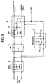
A conventional communication interface is
illustrated in Fig. 9. Referring specifically to Fig. 9,
the communication interface comprises a diode bridge 1
having a terminal connected to a telephone line; a high
pass filter (HPF) 2 having a terminal connected to an output
terminal of the diode bridge 1 on one side; a transmitter/receiver
circuit 3 having a terminal on one side
connected to an output terminal of the HPF 2 and a terminal
on the other side connected to a signal processing
unit; and a power receiving circuit 4 which receives the
output of the diode bridge 1 to supply the transmitter/receiver
circuit 3 with a stabilized direct current
output.
The diode bridge 1, which contains four diodes,
uses a generally called alternating current input side as
a terminal to the telephone line, and a direct current
output side as an opposite terminal.
The HPF 2 includes a capacitor 21 having the
capacitance of approximately 1 µF which is combined with a
terminator of the subsequent transmitter/receiver circuit
3 or of a destination terminal connected through the line
to exhibit an appropriate HPF characteristic.
The transmitter/receiver circuit 3 includes a
transmission amplifier 31, a reception amplifier 32, a
transmission terminator 33, and input resistors 34, 35,
all of which are connected as illustrated to provide a
two-line to four-line conversion function.
The power receiving circuit 4 includes an input
capacitor 41 having a capacitance small enough to exert no
influence on the characteristic of the transmitter/receiver
circuit 3, an output capacitor 42 having a
large capacitance of approximately 1 µF, a resistor 43,
and a Zener diode 44.
The power receiving circuit 4, adapted to
receive an alternating current transmission signal, and
has a signal termination circuit formed in an unbalanced
configuration. Specifically, one of two balanced lines is
referenced, while the other line is driven for transmission,
and a received signal is detected from the other
line during reception.
SUMMARY OF THE INVENTION
A transmission output signal of the transmitter/receiver
circuit 3 has an amplitude generally smaller than
a power supply voltage, so that if the terminal is located
far away from a station, together with its ability of
receiving only a low voltage, a communication available
range is limited.
Also, although the power receiving circuit 4
contains a capacitor of approximately 1 µF to stabilize an
output voltage, it is limited to relatively rough applications
such as a telephone call due to its inherent stability
and noise characteristics.
The application of a high performance voltage
regulator circuit is effective in stabilizing an output
voltage, and a power receiving circuit provided with a
larger output capacitor does increase the stability of the
output voltage. However, as the output voltage increases
the stability, the input impedance of the power supply
becomes smaller than the transmission terminal impedance
in a signal frequency range such as several kHz, as will
be later described, so that the output signal of the
transmitter/receiver circuit 3 is drawn into the power
supply, and accordingly the signal cannot be transmitted.
While a voltage regulator has been implemented
in IC chip and widely used as a three-terminal regulator
and so on, the voltage regulator cannot be used alone in
these applications due to large fluctuations in an input
voltage to the power receiving circuit 4 depending on the
distance between the terminal and a station.
The public communications have become remarkably
pervasive, and a need exists for extending the communication
serviceable range, i.e., increasing the communication
distance. An extended communication distance may be accomplished
by increasing the amplitude of transmission signal.
While a larger amplitude of transmission signal may be
accomplished by increasing a supply voltage, an increase
in supply voltage is limited in the conventional terminal
adapted to operate with the power supplied from the
station.
In view of the problem mentioned above, it is an
object of the present invention to provide a communication
interface apparatus having power receiving means which is
capable of improving the communication performance.
The communication interface apparatus according
to the present invention utilizes any of the following
means alone or some of them in combination.
Transmitting/receiving means is configured in a
balanced circuit so that a sufficient amplitude can be
ensured even if a power receiving circuit provides a low
received voltage.
A low pass filter (LPF) is added in front of the
power receiving circuit to eliminate electrical interference
between the power receiving means and the transmitting/receiving
means, resulting in improved input impedance
frequency characteristics of the power receiving
means.
In the balanced circuit, the LPF is connected to
both plus and minus inputs of the power receiving circuit
such that a bypass capacitor is shared by the plus and
minus inputs, thereby providing a circuit exhibiting well
balanced operation characteristic.
A Zener diode is utilized in the LPF to form a
two-stage stabilizing circuit, so that an IC-based voltage
regulator can be used even with a high input voltage
provided from the power receiving circuit.
BRIEF DESCRIPTION OF THE DRAWINGS
Fig. 1 is a functional block diagram generally
illustrating a line interface circuit according to an
embodiment of the present invention;
Fig. 2 shows the frequency characteristics for
the input impedances of components in the line interface
circuit of Fig. 1;
Fig. 3 a circuit diagram illustrating the line
interface circuit of Fig. 1 in greater detail;
Fig. 4 is a circuit diagram illustrating a line
interface circuit according to another embodiment of the
present invention;
Fig. 5 is a circuit diagram illustrating a line
interface circuit according to a further embodiment of the
present invention;
Fig. 6 is a circuit diagram illustrating a line
interface circuit according to a further embodiment of the
present invention;
Fig. 7 is a functional block diagram illustrating
a line interface circuit according to another embodiment
of the present invention;
Fig. 8 is a functional block diagram illustrating
a further embodiment of the present invention which is
used in a modem system; and
Fig. 9 is a block diagram illustrating a conventional
communication interface.
Fig. 10 is a block diagram illustrating a line
interface circuit according to another embodiment of the
present invention.
DETAILED DESCRIPTION OF THE EMBODIMENTS
The present invention will hereinafter be
described in connection with several embodiments thereof
with reference to the accompanying drawings.
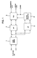
Fig. 1 is a functional block diagram of an
embodiment of the present invention which illustrates a
line interface circuit contained in a modem device for
connection with a telephone line. In the following embodiments,
explanation on a protecting means and a direct
current blocking means is omitted.
Referring specifically to Fig. 1, the illustrated
line interface circuit comprises a diode bridge 1
having a terminal for connection with a telephone line; a
high pass filter (HPF) 2 having a terminal connected with
an output terminal of the diode bridge 1 on one side; a
transmitter/receiver circuit 3 which has a terminal on one
side connected to an output terminal of the HPF 2 and a
terminal on the other side connected to a signal processing
unit; a low pass filter (LPF) 5 which receives the
output of the diode bridge 1 and outputs only a direct
current component; and a voltage regulator (stabilized
power supply) 6 for supplying the transmitter/receiver
circuit 3 with a stabilized direct current output. The LPF
5 and the voltage regulator 6 compose a power receiving
circuit. The diode bridge 1 and the HPF 2 are substantially
similar to those used in a conventional communication
interface previously described in conjunction with
Fig. 9. A protector circuit is omitted in Fig. 1. Also,
in the illustrated circuit, an alternating current transmission
signal superimposed with a direct current voltage
is inputted to the telephone line.
The characteristics of the circuit illustrated
in Fig. 1 will be described with reference to Fig. 2. Fig.
2 shows the frequency characteristics for input impedances
of the HPF 2, LPF 5 and power supply 7. Z1 indicates a
passband impedance of the HPF 2 in which the terminal
impedance of the telephone line appears, and its minimum
value is 600 ohms in direct current resistance. Z2
indicates the off-band impedance value of the LPF 5 which
is tens of kilo-ohms or more. Z3 indicates the passband
impedance value of the LPF 5 which is several ohms or less
in simple characteristic. Z4 indicates the direct current
impedance value of the power supply which is several
hundred kilo-ohms or more. Z5 indicates the input impedance
of the power supply near the signal frequency which
is on the order of several tens of ohms. In Fig. 2, a cut-off
frequency fc is indicated for each of the HPF 2, LPF 5
and power supply 7. Specifically, the cut-off frequency
fc1 of the HPF 2 and the cut-off frequency fc2 of the LPF
6 are set sufficiently lower than the cut-off frequency
fc3 of the voltage regulator 7 (on the order of 1/100 or
less). When observing the impedance from the transmitter/receiver
circuit 3 to the line with the connection
relationship as described above, viewed through the HPF2
are a parallel impedance of an impedance resulting from a
cascade connection of the diode bridge 1, the telephone
line and the station, and an impedance resulting from a
cascade connection of the LPF 5 and the voltage regulator
6.
By designing the configuration and characteristics
of this embodiment as described above, the impedance
observed from the transmitter/receiver circuit 3 is eventually
equal to the impedance value of a line load through
the HPF 2, thus avoiding such a phenomenon that the power
receiving circuit acts as a load to absorb a transmission
signal outputted from the transmitter/receiver circuit 3
in a lower frequency band.
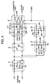
Fig. 3 is a circuit diagram illustrating the
line interface circuit of Fig. 1 in greater detail. Referring
specifically to Fig. 3, the line interface circuit
comprises a diode bridge 1; an HPF 2; a transmitter/receiver
circuit 3; an LPF 5; and a voltage regulator
6. The diode bridge 1 is implemented by Schottky barrier
diodes to reduce an ON-voltage to approximately one half
as much as that of ordinary rectifying diodes. The HPF 2
has 10- µF capacitors 21, 22 in input and output lines,
respectively. The transmitter/receiver circuit 3 includes
transmission amplifier 311, 312; a complementary signal
generator circuit 313; reception amplifiers 314, 315; an
operational amplifier 316; and resistors 317 - 321. The
resistors 317, 320 are 300-ohm terminators. The transmission
amplifiers 311, 312 drive both sides of two lines
(this is called the "balanced driving"). Input signals to
the transmission amplifiers 311, 312 are complementary
signals generated by the complementary signal generator
313 to which a transmission signal is inputted (from a
transmitter data terminal). The resistors 318, 319, which
have the value of 20 kilo-ohms, function to lead a
received signal to one of terminals of the associated
reception amplifiers 314, 315, while the resistors 321,
322 function to lead the transmission signal to the other
terminals of the associated reception amplifiers 314, 315.
Thus, the reception amplifiers 314, 315 act to remove the
transmission signal from the received signal when the
impedance matching is established with the line side. The
outputs of the reception amplifiers 314, 315 are
subtracted in the operational amplifier 316 to remove
common mode noise therefrom, so that only a reception
output signal remains. The LPF 5 is composed of a transistor
51; a common bypass capacitor 52 of approximately 1
µF; a transistor 53; and resistors 54, 55 of several kilo-ohms,
and is configured to connect the collectors of the
transistors 51, 53 on both sides of its input. The cut-off
frequency fc2 of the LPF 5 can be determined by calculating
the time constant from the resistance of the resistor
54 or 55 and the capacitance of the common bypass capacitor
52. The output of the LPF 5 is inputted to the voltage
regulator 6. The voltage regulator 6 is composed of a
Zener diode 62 for generating a reference voltage for the
transistor 61; a bias resistor 63 of approximately 100
kilo-ohms; and an output capacitance 64 of approximately
50 µF.
While the operation of the stabilized power
supply circuit is well known and detailed description
thereon is omitted, the cut-off frequency of the impedance
viewed from the input terminal of the power supply circuit
is as low as on the order of 100 Hz, and merely several
tens of ohms in an audio signal frequency band associated
with modems. However, since the cut-off frequencies of the
HPF 2 and the LPF 5 are at several Hz, the impedance of
the power receiving circuit viewed from the transmitter/receiver
circuit 3 appears as a high impedance of the
HPF2 and the voltage regulator 6 in the vicinity of the
direct current below several Hz, and as an impedance of a
cut-off band of the LPF 5 in the signal frequency band and
higher, so that the power receiving circuit will never
affect the operation of the transmitter/receiver circuit 3.
It should be noted that since the transmitter/receiver
circuit 3 is configured as a balanced circuit,
a transmission power twice higher than that available from
an unbalanced circuit can be obtained from the same power
supply voltage, as long as the balanced and unbalanced
circuits employ the same internal circuit for their transmission/reception
amplifiers. While it has been conventionally
known that the balanced circuit exhibits such
characteristics, there is not a known example in which a
balanced LPF circuit as embodied in the present invention
is applied in a circuit which supplies a transmitter/receiver
circuit with electric power received from a
line.
The LPF 5 implemented by a balanced circuit
shares the bypass capacitor for both plus and minus inputs
of the power receiving circuit. Such a configuration
causes a bypass signal to act also on the circuit on the
opposite side to provide an inexpensive circuit which
however has good operational balance characteristics.
While this embodiment shows the simplest example
of the voltage regulator 6, other high performance
circuits may of course be used in the line interface
circuit of the present invention. Such high performance
voltage regulators may be those including a controlling
transistor having a high amplification ratio and exhibiting
a good controllability; a reference voltage source
having good accuracy and temperature characteristics; an
error amplification configuration for detecting the
difference between an output voltage and a set voltage to
adjust a controlling transistor; and/or a protector
circuit for detecting an excessive voltage or an excessive
current to protect associated circuits. Such alternative
voltage regulators may be implemented irrespective of the
form, i.e., in discrete or integrated circuit.
In this embodiment, a protector circuit is
omitted, as previously mentioned.
Fig. 4 is a circuit diagram illustrating a line
interface circuit according to another embodiment of the
present invention. The line interface circuit of Fig. 4 is
identical to that of Fig. 3 except for the LPF 5. The
reference numerals in Fig. 4 designate the corresponding
components or functions in Fig. 3. The LPF 5 in Fig. 4
differs from the counterpart in Fig. 3 and is characterized
in that the bypass capacitor 52 is replaced with a
Zener diode (voltage regulating element) 57 having a
breakdown voltage of 12 volts, and a small output capacitance
58 of approximately 10 nF is additionally connected.
Since the resulting circuit configuration acts not only as
an LPF, but also as a stabilized power supply having an
output voltage of 12 volts and a high cut-off frequency
fc3, the input voltage requirements to the voltage regulator
6 can be relieved.
Fig. 5 is a circuit diagram illustrating a line
interface circuit according to a further embodiment of the
present invention, where the same reference numerals as
those in Fig. 3 designate the same components or functions.
The line interface circuit of Fig. 5 is characterized by
an unbalanced circuit configuration, where the negative
output of the diode bridge 1 is connected in common
through an HPF 2, a transmitter/receiver circuit 3, an LPF
5, and a voltage regulator 6. In this way, since the HPF 2,
transmitter/receiver circuit 3 and LPF 5 may be applied
only to the positive output of the diode bridge 1, the
line interface circuit of Fig. 5 is advantageous in that
the number of circuit elements can be reduced. It should
be noted that while the transmitter/receiver circuit 3 in
an unbalanced circuit configuration is inferior in driving
capability to the counterpart in a balanced circuit
configuration, the inferior driving capability will not
cause any problem if the driving capability is improved by
any appropriate method such as a BiCMOS device, a rail-to-rail
amplifier circuit or the like, or if the communication
interface is applied to a line of a short distance
from a station which can be accommodated within the driving
capability of the transmitter/receiver circuit 3.
As one implementation of the LPF, a chalk coil
circuit having a core wound with wires may be used. In
addition, a so-called electronic chalk coil circuit, which
is formed of transistors, resistors and a capacitor, is
also known (see for example, "Design of Stabilized Power
Supply Circuit," third edition, published by CQ publications
on April 20, 1972, Fig. 5.5(d) on page 76, and JP-A-9-200388).
Fig. 6 is a circuit diagram illustrating a line
interface circuit according to a further embodiment of the
present invention, where the same reference numerals as
those in Fig. 5 designate the same components or functions.
An LPF 5 in Fig. 6 differs from the counterpart in Fig. 5
and is characterized in that the bypass capacitor 52 is
replaced with a Zener diode (voltage regulating element)
57 having a breakdown voltage of 12 volts, and a small
output capacitance 58 of approximately 10 nF is additionally
connected. Since the resulting circuit configuration
acts not only as an LPF, but also as a stabilized power
supply having an output voltage of 12 volts and a high
cut-off frequency fc3, the input voltage requirements to a
voltage regulator 6 can be relieved.
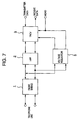
Fig. 7 is a functional block diagram illustrating
a line interface circuit according to another embodiment
of the present invention. In Fig. 7, a diode bridge 1,
an HPF 2 and a transmitter/receiver circuit 3 are identical
in function to those in Fig. 1. An improved voltage
regulator 7, which is a combination of low pass filtering
and voltage regulation functions, simplifies the entire
communication interface in configuration as illustrated,
making it suitable for implementation as a an IC-based or
a modular unit.
Fig. 8 is a functional block diagram illustrating
a further embodiment of the present invention which is
used in a modem system. In Fig. 8, components 1 - 6 are
identical in name and function to the counterparts in Fig.
1. The modem system of Fig. 8 additionally comprises an
audio codec 8 containing an analog-to-digital converter
(ADC) and a digital-to-analog converter (DAC); an isolator
9 for transmitting a signal while isolating an input
terminal from an output terminal; a digital filter 110; a
signal processing unit 120 represented by a host CPU
(Central Processing Unit) such as a digital signal processor
(DSP), a reduced instruction set processor (RISC) or
the like, including a power supply; surge absorbing
capacitors 15, 16; and a ground terminal FG which is a
frame ground.
The isolator 9 is a circuit block which electrically
isolates two circuits from each other but couples a
signal between the two circuits. When the isolator 9 is
utilized, an analog front end (AFE) can be created without
using an insulating transformer. The analog front end is
an interface Circuit for a signal processing device, which
generally includes ADC for converting an analog signal to
a digital signal and/or DAC for converting a digital
signal to an analog signal; a bandpass filter means; a
level adjusting means; and so on, and is used for a line
interface circuit in a modem. In the field of communications,
a high isolation property is required to the boundary
between a network and a terminal (hereinafter called
the "line network") for protecting highly public network
facilities and terminals, and small transformers having
high isolation properties for communications have been
conventionally used to meet the requirement. However, with
increasingly widespread personal terminals, a further
reduction in size and weight has been required to transformers
for use in portable terminals. The requirement to
a reduction in size implies problems which cannot be
sufficiently responded only by improving the material and
structure used in the transformer, so that the application
of isolator in personal terminals has been taken into
account. Also, for applications in measurement and medical
fields, and so on, isolation is often required between a
signal detecting portion and a signal processing portion,
such as between a sensor and a signal processing circuit,
in which case an isolating coupler is known as an isolating
or separating means.
While required characteristics are different,
the isolator may be inserted between the transmitter/receiver
circuit 3 and the audio codec 8. It should be
noted that not only the components 1 - 6 but also the
components 8, 9 on the telephone line side may be
connected to operate with electric power outputted by the
power receiving circuit 6.
For transmitting a signal through the modem
system, a terminal on the telephone line side is connected
to the telephone line, the signal processing unit 120 is
powered on to generate a digital modulated signal which is
passed through an up-channel of the digital filter 110, an
up-channel of the isolator 9, and the DAC of the codec 8
to generate an analog transmission signal which is
inputted to a transmitter data terminal of the transmitter/receiver
circuit 3. In this way, the circuit components
1 - 8 on the line side become operative to
efficiently deliver the transmission signal to the
telephone line as previously described in conjunction with
Fig. 1. Upon reception, the components may be similarly
connected, causing a received signal inputted to the
terminal on the telephone line side to appear at a receive
data terminal as previously described in conjunction with
Fig. 1. Thus, the received signal is converted by the ADC
of the codec 8 to a digital signal which is passed through
a down-channel of the isolator 9 and a down-channel of the
digital filter 110, and inputted to the signal processing
unit 120. In the signal processing unit 120, the received
signal undergoes processing such as demodulation to eventually
provide received data.
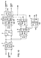
Fig. 10 is a circuit diagram showing another
embodiment of a modem to which the present invention is
applied. In Fig. 10, reference numerals 1-322 indicate
elements having the same function as those in Fig. 6. A
reference numeral 130 indicates an DC termination circuit,
131 to 133 resistors, 134 a capacitor and 135 a transistor.
The DC termination circuit 130 is formed of a well-known
circuit block. The transistor 135 is used to select a
large amplification characteristic of the transistor. The
resistors 131 and 132 serve as a bias circuit for the
transistor and the resistor 132 is connected to the
capacitor 134. The resistor 133 is a load for transistor
135. In operation of the termination circuit 130, when the
modem is connected to the line, the termination circuit
130 flows only a DC current in response to application of
a relevant voltage and exhibits a high impedance to a T
transmission signal which is an AC current. The high
impedance capability to AC current depends on the capacitor
134 and the amplification factor of the transistor 135.
This circuit is similar to the LPF means stated
above. Accordingly, an AC impedance characteristic can be
relaxed by providing the LPF means and the power receiving
circuit. As a result, the capacitor 134 may be dispensed
with or may have a small capacitance value. In other words,
the size and the cost of the modem can be reduced.
The DC termination circuit can be integrally
combined with the LPF means or the power receiving means.
In that case, such combination may contribute the small-sized
and low-cost modem, to advantage.
As described above, according to the present
invention, an output signal having a large amplitude can
be produced even from a low received voltage by the use of
a balanced driving circuit, a BiCMOS device, a rail-to-rail
driving circuit as a circuit configuration having a
high driving performance. Also, an LPF added to a power
receiving circuit results in improved input impedance
frequency characteristics of the power receiving circuit,
and improved output characteristics of a transmitter/receiver
circuit. Further, the balanced driving
circuit employs an LPF applied to both plus and minus
inputs of the power receiving circuit, and a shared bypass
capacitor to provide a circuit configuration which is
inexpensive but has well balanced operational characteristics.
Moreover, an LPF using a Zener diode is added to a
voltage regulator to provide an inexpensive two-stage
stabilizing circuit, in an IC chip, including low pass
filtering and voltage regulating functions, which can
accommodate a high input voltage from the power receiving
circuit.
The arrangement of a DC termination circuit
between the LPF means and the power receiving means can
also contribute to reduce the size and cost of the modem.