EP1069734A2 - Distributed service request bus using tokens to resolve collisions - Google Patents
Distributed service request bus using tokens to resolve collisions Download PDFInfo
- Publication number
- EP1069734A2 EP1069734A2 EP00202514A EP00202514A EP1069734A2 EP 1069734 A2 EP1069734 A2 EP 1069734A2 EP 00202514 A EP00202514 A EP 00202514A EP 00202514 A EP00202514 A EP 00202514A EP 1069734 A2 EP1069734 A2 EP 1069734A2
- Authority
- EP
- European Patent Office
- Prior art keywords
- data
- node
- service request
- transfer
- downstream
- Prior art date
- Legal status (The legal status is an assumption and is not a legal conclusion. Google has not performed a legal analysis and makes no representation as to the accuracy of the status listed.)
- Granted
Links
Images



Classifications
-
- H—ELECTRICITY
- H04—ELECTRIC COMMUNICATION TECHNIQUE
- H04L—TRANSMISSION OF DIGITAL INFORMATION, e.g. TELEGRAPHIC COMMUNICATION
- H04L12/00—Data switching networks
- H04L12/28—Data switching networks characterised by path configuration, e.g. LAN [Local Area Networks] or WAN [Wide Area Networks]
- H04L12/40—Bus networks
- H04L12/407—Bus networks with decentralised control
- H04L12/417—Bus networks with decentralised control with deterministic access, e.g. token passing
-
- G—PHYSICS
- G06—COMPUTING OR CALCULATING; COUNTING
- G06F—ELECTRIC DIGITAL DATA PROCESSING
- G06F13/00—Interconnection of, or transfer of information or other signals between, memories, input/output devices or central processing units
- G06F13/14—Handling requests for interconnection or transfer
- G06F13/36—Handling requests for interconnection or transfer for access to common bus or bus system
- G06F13/368—Handling requests for interconnection or transfer for access to common bus or bus system with decentralised access control
- G06F13/37—Handling requests for interconnection or transfer for access to common bus or bus system with decentralised access control using a physical-position-dependent priority, e.g. daisy chain, round robin or token passing
Definitions
- the technical field of this invention is digital device functional blocks which relates generally to the area of microprocessor design and relates more specifically to the area of digital signal processor devices.
- this invention relates to distributed service request busses such as data transfer request busses.
- the present invention deals with the data transfer connecting various memory port nodes as applied to the transfer controller with hub and ports architecture.
- the transfer controller with hub and ports is the subject of U.K. Patent Application serial number 9909196.6 filed April 21, 1999 having an EPO convention Patent Application No. 00303373.5 filed April 20, 2000.
- the transfer controller with hub and ports is a significant basic improvement in data transfer techniques in complex digital systems and provides many useful features, one of which is the internal memory port which allows connection of a virtually unlimited number of processor/memory nodes to a centralized transfer controller.
- the centralized transfer controller must be able to transfer data from node to node with performance relatively independent of how near or remote a node might be from the transfer controller itself. To clarify the problem solved by the present invention, it is helpful to review the characteristics, architecture, and functional building blocks of the transfer controller with hub and ports.
- the system problem addressed by this invention is that of sending service transaction requests from many sources.
- the many sources may be on a single silicon chip.
- the transaction requests are sent to a common central resource such as a conventional direct memory access controller.
- this direct memory access controller is the transfer controller with hub and ports of the above named patent application.
- the service requests are contained in transaction request packets composed of words, each of which may be many bits wide.
- Non-parallel transaction processing is an alternative. This requires a centralized arbiter to determine order of servicing on service request collisions. This alternative must also force each non-serviced source to re-submit requests until acknowledged and handled. With either parallel or non-parallel transaction processing, the transaction processor would require extensive modifications for each new design adding or removing requestors. This results in poor reusability of chip module designs, making poor use of the scarce resource of design engineers. Additionally, requestors distant from the centralized transaction processor would have longer buses. This requires extra design attention or hardware to ensure that signal paths would not be slow.
- the transfer controller with hub and ports is a unique mechanism which consolidates the functions of a direct memory access and other data movement engines in a digital signal processor system (for example, cache controllers) into a single module.
- the transfer controller with hub and ports to which this invention relates, is a highly parallel and highly pipelined memory transaction processor.
- This transfer controller with hub and ports serves as a backplane to which many peripheral and/or memory ports may be attached.
- any station can start transmitting when it sees no activity on the network. However, in the unarbitrated state, it is possible for multiple stations to start transmitting simultaneously. Stations do not negotiate for ownership of the network. Instead stations check for the conflicting condition by receiving back what was transmitted, and checking to see if it has been corrupted (indicating a collision with another station). If this happens, all stations that started transmission simultaneously will detect the collision and abort their transmission. These stations then wait a random amount of time before attempting to start transmitting again. As each station will pick a random delay, each station eventually gets to transmit its data. Over time this system could provide fair access to all stations.
- a station can start transmitting only if it has the token. When it has finished, it passes the token to the next station, which can either take it and transmit data, or pass the token on again if it is not ready to transmit. This system is very fair, but is somewhat more complex and costly to implement.
- a centralized data transfer controller handling multiple simultaneous data transfer requests must be designed to manage the number of independent data transfer requests in a manner which solves these collision incidents unequivocally and any system design faces obvious compromises.
- This invention provides the solution to collision arbitration with fairness on a network of transfer request nodes.
- the network consists of one transfer request node per transfer requestor, arranged in a transfer request bus.
- the transfer request bus starts at an upstream node and terminates downstream at a receiver node referred to as the request bus master input.
- the previous upstream node can transmit a transfer request to the present node, which it retransmits downstream.
- the requestor attached to the present node itself can transmit a request to the next downstream node. Arbitration of which is to occur is done by a token passing scheme.
- a token signal is active at only one node on the transfer request bus. This token is passed in a downstream direction around the transfer request nodes of the bus on each clock cycle. Thus one and only one transfer request node holds the token at any given time. The token is passed from the extreme downsteam request node to the extreme upstream request node to form a token loop.
- Arbitration of requests takes place as follows. If the present node is not ready to insert a transfer request from its transfer requestor, then any upstream request is transmitted to the present node. This happens independent of whether the present node has the token. If the present node is ready to insert a request, it cannot occur except under certain conditions. If there is no request from a upstream node, then the present node may transmit its request downstream regardless of whether it has the token. If the present node receives a request from the immediate upstream node, then its action depends upon whether it holds the token. If the present node does not hold the token, then it must retransmit the request signal from the upstream node. If the present node holds the token, then it can transmit its own request. In this case the present node, sends a stall signal to the next upstream node, stalling its request. No requests are aborted. Any previously stalled upstream requests may proceed as soon as the token passes from the present node.
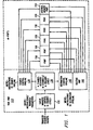
- Figure 1 illustrates a block diagram of the basic features of the transfer controller with hub and ports.
- the transfer controller with hub and ports is basically a data transfer controller which has at its front end portion, a queue manager 100 receiving, prioritizing, and dispatching data in the form of transfer request packets.
- This queue manager 100 connects within the hub unit 110 to the channel registers 120.
- Channel registers 12 receives the data transfer request packets and processes them first by prioritizing them and assigning them to one of the N channels. Each channel represents a priority level.
- These channel registers 120 interface with the source control pipeline 130 and destination control pipeline 140. These are address calculation units for source (read) and destination (write) operations.
- Outputs from these pipelines are broadcast to M Ports (six shown in Figure 1 as 150 through 155).
- the ports 150 to 155 are clocked either at the main processor clock frequency or at a lower external device clock frequency.
- Read data from one port, e.g. port 150, having a destination write address of port 153 is returned to the hub destination control pipeline through the routing unit.
- the transfer controller with hub and ports introduces several new ideas supplanting the previous transfer controller technology.
- the transfer controller with hub and ports contains multiple external ports, all of which look identical to the hub. Thus peripherals and memory may be freely interchanged without affecting the transfer controller with hub and ports.
- the transfer controller with hub and ports concurrently executes transfers. That is, up to N transfers may occur in parallel on the multiple ports of the device, where N is the number of channels in the transfer controller with hub and ports core. Each channel in the transfer controller with hub and ports core is functionally just a set of registers.
- the transfer controller with hub and ports includes a mechanism for queuing transfers up in a dedicated queue RAM.
- FIG. 2 illustrates from a higher level an overview of an multiprocessor integrated circuit employing the transfer controller with hub and ports of this invention.
- the transfer controller with hub and ports 220 and the ports including ports external port interface units 230 to 233 and internal memory port 260, are the first two main functional blocks. Though four external port interface units 230, 231, 232 and 233 are illustrated, this is an example only and more or less could be employed.
- the other two main functional blocks are the transfer request feed mechanism 245 and the data transfer bus (DTB) 255. These are closely associated functional units that are but not a part of the transfer controller with hub and ports 220. Transfer request feed mechanism 245 is coupled to plural internal memory port nodes 270, 271 and 272.
- Each of these internal memory port nodes preferable includes an independently programmable data processor, which may be a digital signal processor, and corresponding cache memory or other local memory.
- the internal construction of these internal memory port nodes 270, 271 and 272 is not important for this invention. For the purpose of this invention it sufficient that each of the internal memory port nodes 270, 271 and 272 can submit transfer requests via transfer request feed mechanism 245 and has memory that can be a source or destination for data. Transfer request feed mechanism 245 prioritizes these packet transfer requests.
- Transfers originating from or destined for internal memory port nodes 270, 271 or 272 are coupled to transfer controller with hub and ports 220 via data transfer bus 255 and internal memory port master 260.
- Figure 2 highlights the possible connection of data transfer bus 255 to multiple internal memory port nodes 270, 271 and 272 and the possible connection of multiple transfer request nodes to transfer request feed mechanism 245.
- the transfer controller with hub and ports need not be modified if the number of transfer requestors is changed.
- the transfer controller with hub and ports design can be highly modular.
- the modularity of the transfer request bus is a significant component of the modularity of the transfer controller with hub and ports.
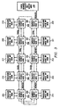
- FIG. 3 illustrates the connection of transfer request nodes in a bus with nodes labeled 300 through 309.
- Node 300 being nearest to the queue manager request bus master input 320, is referred to as the nearest or most downstream node.
- Node 309 is referred to as the farthest or most upstream node.
- a processor/cache internal memory node (nodes 310 through 319) is attached. These processor cache internal memory nodes 310 to 319 are the same as processor/cache internal memory nodes 270, 271 and 272 illustrated in Figure 2. Each of these processor/cache internal memory nodes has the capability for placing local transfer requests on the bus.
- transfer requests are passed from one node downstream to the next node. Such transfer requests ultimately reach queue manager request bus master input 320 for service of the transfer request.
- An upstream request has priority for being passed onward until a local request becomes active.
- the transfer request node determines if the token is present. If not, the local request stalls.
- the token is simply a signal circulated in the upper path, marked “token” in Figure 3, around the transfer request nodes. The token moves one position each clock cycle. This movement is downstream like the transfer requests. After reaching transfer request node "0" 300, the token wraps around to transfer request node "9" 309.
- the upstream request must be stalled to allow the local request to take priority.
- any local request may be placed on the local transfer request node regardless of the presence of the token.
- the middle path marked "stall” carries the individual stalls which hold off upstream requests in favor of local requests having the token.
- the lower path marked "requests” in Figure 3 represents the flow of "requests" from upstream nodes toward downstream nodes.
- FIG 4 illustrates the basic structure for a transfer request node 300.
- Each transfer request node 300 to 309 preferably has this structure.
- the request path illustrated in Figure 3 is divided into a request path and a transfer request packet path.
- Each request for service preferably includes both a request and data in a packet.
- the packet indicates the data to be transferred by, for example, source and destination addresses and data size.
- Local requests for service from the corresponding processor/cache internal memory port node 310 to 318 are received on local request input 401 and local transfer data packets 407 are received on local data input 400.
- Requests for service from upstream nodes are received on upstream request input 402 and upstream transfer data packets 417 are received on upstream data input 404.
- Transfer request node control block 410 also receives the token on upstream token input 404 and a downstream stall signal from a downstream node on downstream stall input 421. Transfer request node control block 410 produces a downstream request signal on downstream request output 422, an upstream stall signal on upstream stall output 403, a local stall signal on local stall output 418 and supplies the token to the downstream node on downstream token output 419.
- Transfer request packet registers and recirculation logic 411 receives local transfer data packet 407 and upstream transfer data packet 417. Transfer request packet registers and recirculation logic 411 supplies downstream data packet 408 to the downstream node on transfer data packet output 409. Transfer request packet registers and recirculation logic 411 also includes a local data recirculation path 414 and an upstream data recirculation path 416. The local data packet recirculates during a local stall. Similarly, the upstream data packet recirculates during an upstream stall.
- Transfer request node control block controls operation of the transfer request node as shown in Table 1. Inputs Outputs Upstream Request Local Request Token Downstream Request Upstream Stall Local Stall No No ----- None No No Yes No ----- Upstream Request No No Yes Yes Absent Upstream Request No Yes Yes Yes Present Local Request Yes No No Yes ----- Local Request No No No
- the transfer request node control block receives a transfer request from both the upstream node and the current node, the presence or absence of the token is not relevant.
- the token is used only to resolve priority when both an upstream request and a local request occur simultaneously. Accordingly, Table 1 shows a "----" or "don't care” status for the token for these conditions.
- FIG. 5 illustrates a block diagram of an example of a preferred processor and cache memory combination implementing the internal memory nodes 270, 271 and 272 of Figure 2.
- Each internal memory node 270, 271 and 272 preferably includes a digital signal processor core and corresponding instruction and data cache memory.
- Transfer controller with hub and ports 220 provides for all data communication among internal memory nodes 270, 271 and 272, external input/output (I/O) devices and peripherals at external ports 230 to 233, and internal memory at internal memory port master 260.
- I/O input/output
- Each internal memory node 270, 271 and 272 preferably comprises a very long instruction word (VLIW) digital signal processor core 44, program memory controller (PMC) 46, data memory controller (DMC) 48, an emulation, test, analysis and debug block 50, local memory and data transfer bus (DTB) interface 52.
- VLIW very long instruction word
- PMC program memory controller
- DMC data memory controller
- DTB local memory and data transfer bus
- Internal memory nodes 270, 271 and 272 and transfer controller with hub and ports 220 communicate over a pair of high throughput buses.
- Transfer request feed mechanism 245 is used by digital signal processor cores 44 to specify and request transactions in transfer controller with hub and ports 220.
- Data transfer bus (DTB) 255 is used to load and store data from objects in the global memory map.
- any given digital signal processor core 44 can access its own internal local memory within the cluster without permission from transfer controller with hub and ports 220, any access to global memory outside of its local memory requires a transfer controller directed data transfer, whether the access is to external memory or to another digital signal processor local memory.
- the overall architecture is scalable, allowing for the implementation of many internal memory nodes, although three is currently the preferred embodiment. It should be noted that architectural details, such as the number of digital signal processor cores, and their instruction set architectures are not essential to the invention. This microprocessor architecture is exemplary only, and the invention is applicable to many microprocessor architectures.
- FIG. 6 is a block diagram illustrating more detail of digital signal processor core 44 illustrated in Figure 5.
- Digital signal processor core 44 is a 32-bit eight-way VLIW pipelined processor.
- the instruction set consists of fixed length 32-bit reduced instruction set computer (RISC) type instructions that are tuned for digital signal processing applications. Almost all instructions perform register-to-register operations and all memory accesses are performed using explicit load/store instructions.
- instruction pipeline 58 consists of fetch stage 60 and decode stage 62.
- Fetch stage 60 retrieves program codes into the processor core from instruction cache 64 under control of program memory controller 46 in groups of eight instructions called a fetch packet.
- Decode stage 62 parses the fetch packet, determines parallelism and resource availability and constructs an execute packet of up to eight instructions.
- Execution pipeline 66 consists of two symmetrical datapaths, datapath A 68 and datapath B 70, a common 64-bit load/store unit group D-unit group 72, and a common branch unit group P-unit group 74.
- Each datapath contains 32-word register file (RF) 76, and four execution unit groups, A-unit group 78, C-unit group 80, S-unit group 82, and M-unit group 84.
- RF register file
- the memory at internal memory nodes 270, 271 and 272 is preferably partitioned between instruction cache memory 64 controlled via program memory controller 46 and data cache memory and random access memory 88 controlled via data memory controller 48. These memory partitions are employed by digital signal processor core 44 in a conventional manner.
- Each digital signal processor core 44 may request data transfers in is several ways.
- Digital signal processor core 44 may issue a data transfer request to transfer controller with hub and ports 220 in response to an explicit data transfer instruction.
- the data transfer instruction must specify the data source, the data destination and the data amount. These specifications may be by immediate fields in the instructions or by parameters stored in registers or memory. It is preferable that each digital signal processor core 44 be capable of requesting any data transfer that can be serviced by transfer controller with hub and ports 220. Thus any digital signal processor core 44 may transfer data internally or externally and load or read any internal memory node.
- Each digital processor core 44 preferably also includes automatic mechanisms for generating requests for data transfer for cache service.
- an instruction cache miss preferably causes program memory controller 46 to generate a data transfer request from another data source to fill a line of instruction cache 64 with data including program instructions stored at the address generating the cache miss.
- a data cache miss on a data read preferably causes data memory controller 48 to generate a data transfer request to retrieve data to fill a line in data cache/random access memory 88 with corresponding data.
- These instruction and data are stored in a higher level of memory. This higher level of memory may be an on-chip combined cache used by all digital signal processor cores 44 or it may be external to the multiprocessor integrated circuit. There are two alternatives for data cache misses on data writes.
- a data write by digital processor core 44 that misses data cache/random access memory 88 causes data memory controller 48 to generate a data transfer request to store the write data in the appropriate location in a higher level of memory.
- a data write by digital processor core 44 that misses data cache/random access memory 88 causes data memory controller 48 to generate a data transfer request to recall corresponding data in the appropriate location from a higher level of memory for storage in data cache/random access memory 88.
- the write data is then written into data cache/random access memory 88 overwriting the corresponding data just recalled from the higher level of memory. This process is referred to as write allocation within the data cache.
- Data memory controller 48 preferably also employs a data transfer request to handle data writeback to a higher level memory upon cache eviction of a dirty entry.
- a dirty cache entry includes data that has been modified since it was recalled from a higher level of memory. This modified data corresponds to a later state of the program than the data stored in the higher level of memory. When such data must be replaced to make room for new cache data, referred to as cache eviction, this dirty data must be written back to the higher level of memory to maintain the proper program state.
- Transfer controller with hub and ports 220 is preferably employed for this writeback of evicted dirty cache entries.
- This priority technique operates fairly under a variety of loading conditions. When loading is light and there is a low probability of generating a local request or receiving an upstream request, there are few collisions. Under these conditions nearly all local requests are immediately transmitted downstream. During moderate loading the upstream nodes have a greater probability of passing to the queue master node but are further away than the downstream nodes. During heavy loading when there is a high probability of both receiving an upstream request and generating a local request, the token ensures each node has fair access. Thus the priority technique of this invention provides generally fair access to all nodes under all conditions. This technique is scalable by the selection of the number of nodes. The loading on each node is independent of the number of nodes because each node connects to only its neighbors.
- This invention has been described in conjunction with the preferred embodiment in which the requests are for data transfer. Those skilled in the art would realize that this type request is not only type that can be serviced by this invention.
- This invention can be used to connect and prioritize any data processing function that can be requested by plural requestors and is serviced by a central application unit.
Landscapes
- Engineering & Computer Science (AREA)
- Theoretical Computer Science (AREA)
- Physics & Mathematics (AREA)
- Signal Processing (AREA)
- General Engineering & Computer Science (AREA)
- General Physics & Mathematics (AREA)
- Computer Networks & Wireless Communication (AREA)
- Multi Processors (AREA)
- Small-Scale Networks (AREA)
- Computer And Data Communications (AREA)
- Bus Control (AREA)
- Saccharide Compounds (AREA)
- Air Bags (AREA)
Abstract
Description
| Inputs | Outputs | ||||
| Upstream Request | Local Request | Token | Downstream Request | Upstream Stall | Local Stall |
| No | No | ----- | None | No | No |
| Yes | No | ----- | Upstream Request | No | No |
| Yes | Yes | Absent | Upstream Request | No | Yes |
| Yes | Yes | Present | Local Request | Yes | No |
| No | Yes | ----- | Local Request | No | No |
Claims (19)
- A method of scheduling service requests from a plurality of nodes, each capable of generating a service request, said method comprising the steps of:disposing the plurality of nodes in a chain having an upstream most node and a downstream most node, said downstream most node connected to application device capable of servicing the service requests;sequentially passing a token among the plurality of nodes from the upstream most node to the downstream most node following the chain, said token passing from the downstream most node to the upstream most node in a loop;determining at each node whether a service request is received from a next upstream node;determining at each node whether that node generates a service request;determining at each node whether that node holds the token;passing a service request received at one of the plurality of nodes from a next upstream node to a next downstream node if that node does not generate a service request, the downstream most node passing the service request to the application device;passing a service request received at one of the plurality of nodes from the next upstream node to the next downstream node if that node generates a service request and that node does not hold the token;passing a service request generated by a node to the next downstream node if that node generates a service request and does not receive a service request from the next upstream node; andpassing a service request generated by a node to the next downstream node if that node generates a service request and that node holds the token.
- The method of claim 1, wherein:sending a stall signal from a node to the next upstream node if that node generates a service request, holds the token and receives a service request from the next upstream node or if that node receives a stall signal from the next downstream node; andstalling passing a service request from a node to the next downstream node if that node receives a stall signal.
- The method of claim 1, wherein:said service requests are data transfer requests for transfer of data; andtransferring data under control of said application device in response to receipt of a data transfer request.
- The method of claim 3, wherein:said step of generating a data transfer request generates an indication of source address, an indication of destination address and an indication of data amount.
- The method of claim 3, wherein each of the plurality of nodes includes a data processor and an instruction cache for temporarily storing program instructions controlling the data processor, the method further comprising:generating at a node a data transfer request for program cache fill from a system memory upon a read access miss to the instruction cache of that node;transferring data under control of said application device from a system memory to the instruction cache of a node generating a data transfer request for program cache fill.
- The method of claim 3, wherein each of plurality of nodes includes a data processor and a data cache for temporarily storing data employed by the data processor, further comprising:generating at a node a data transfer request for data cache fill from a system memory upon a read access miss to said data cache of that node; andtransferring data under control of said application device from a system memory to the data cache of a node generating a data transfer request for data cache fill.
- The method of claim 3, wherein each of the plurality of nodes includes a data processor and a data cache for temporarily storing data employed by the data processor, further comprising:generating at a node a data transfer request for data writeback to a system memory upon a write miss to said data cache of that node; andtransferring data under control of said application device from a node generating a data transfer request for data writeback to the system memory.
- The method of claim 3, wherein each of the plurality of nodes includes a data processor and a data cache for temporarily storing data employed by the data processor, further comprising:generating at a node a data transfer request for write data allocation from a system memory to said data cache upon a write miss to said data cache of that node; andtransferring data under control of said application device from a system memory to the data cache of a node generating a data transfer request for write data allocation.
- The method of claim 3, wherein each of the plurality of nodes includes a data processor and a data cache for temporarily storing data employed by the data processor, further comprising:generating at a node a data transfer for data writeback to said system memory upon eviction of dirty data from the data cache of that node; andtransferring data under control of said application device from a node generating a data transfer request for eviction of dirty data to the system memory.
- A data processing apparatus comprising:an application device capable of servicing requested data processing operations in response to corresponding service requests;a plurality of nodes disposed in a chain having an upstream most node and a downstream most node, each of said plurality of nodes havingan operation unit capable of generating service requests,a token input for receiving a token from a next upstream node in said chain, said token input of said upstream most node receiving said token from said downstream most node,an upstream service request input for receiving a service request from a next upstream node in said chain, said upstream most node not receiving any signal on said upstream service request input,a local service request input for receiving a service request from said operation unit,a token output for supplying said token to a next downstream node in said chain, said downstream most node supplying said token to said token input of said upstream most node,a downstream service request output for supplying a service request to a next downstream node in said chain, said downstream most node supplying said service request to said application device,a control block connected to said token input, said token output, said upstream service request input, said local service request input and said downstream service request output, said control block operative topass said token from said upstream most token input to said downstream token output,pass a service request received at said upstream service request input to said downstream service request output if that node does not generate a local service request, the downstream most node passing the service request to the application device;pass a service request received at said next upstream service request input to said downstream service request output if that node generates a local service request and that node does not hold the token;pass a local service request to said downstream service request output if that node generates a local service request and does not receive a service request from said upstream service request input; andpass a local service request to said downstream service request output if that node generates a local service request and that node holds the token.
- The data processing system of claim 10, wherein: each node further includesa downstream stall input for receiving a stall signal from a next downstream node, said downstream most node not receiving any signal on said downstream stall input, andan upstream stall output for supplying a stall signal to said downstream stall input of a next upstream node, said upstream stall output of said upstream most node not connected; and wherein said control block is further operative togenerate a stall signal on said upstream stall output if that node generates a local service request, receives a service request from said upstream service request input and that node holds the token or if that node receives a stall signal from said next downstream node, andstall supply of a service request on said downstream service request output if that node receives a stall signal on said downstream stall input.
- The data processing system of claim 10, further comprising:a system memory connected to said application device;
wherein said operation unit of each node is capable of generating data transfer service requests; and
wherein said application device is capable of transferring data with said system memory in response to data transfer service requests. - The data processing system of claim 12, wherein:said operation unit of each node is capable of generating said data transfer service requests including a transfer data packet including an indication of source address, an indication of destination address and an indication of data amount;each node further includesa transfer data packet input for receiving a transfer data packet from a next upstream node, said upstream most node not receiving any signal on said transfer data packet input, anda transfer data packet output for supplying a transfer data packet to a said transfer data packet output of a next downstream node, said transfer data packet output of said downstream most node connected to said applications device; andsaid applications device controlling data transfer from an address corresponding to said indication of source address, to an address corresponding to said indication of destination address and in an amount corresponding to said indication of data amount.
- The data processing system of claim 12, wherein:each of said plurality of nodes includes a data processor and an instruction cache for temporarily storing program instructions controlling said data processor, said data processor generating a data transfer service request for program cache fill from said system memory upon a read access miss to said instruction cache; andsaid application device transferring data from said system memory to said instruction cache of a node generating a data transfer request for program cache fill.
- The data processing system of claim 12, wherein:each of said plurality of nodes includes a data processor and a data cache for temporarily storing data employed by said data processor, said data processor generating a data transfer service request for data cache fill from said system memory upon a read access miss to said data cache;said application device transferring data from said system memory to said data cache of a node generating a data transfer request for data cache fill.
- The data processing system of claim 12, wherein:each of said plurality of nodes includes a data processor and a data cache for temporarily storing data employed by said data processor, said data processor generating a data transfer service request for data writeback to said system memory upon a write miss to said data cache; andsaid application device transferring data from said data cache of a node generating a data transfer service request for data writeback to said system memory.
- The data processing system of claim 12, wherein:each of said plurality of nodes includes a data processor and a data cache for temporarily storing data used by said data processor, said data processor generating a data transfer service request for write data allocation from said system memory to said data cache upon a write miss to said data cache; andsaid application device transferring data from said system memory to said data cache of a node generating a data transfer service request for write data allocation.
- The data processing system of claim 12, wherein:each of said plurality of nodes includes a data processor and a data cache for temporarily storing data used by said data processor, said data processor generating a data transfer for data writeback to said system memory upon eviction of dirty data from said data cache;said application device transferring data from to said data cache of a node generating a data transfer service request for data writeback to said system memory.
- The data processing system of claim 12, wherein:said application device and said plurality of nodes are disposed on a single integrated circuit.
Applications Claiming Priority (2)
| Application Number | Priority Date | Filing Date | Title |
|---|---|---|---|
| GB9916704 | 1999-07-16 | ||
| GB9916704A GB2352143A (en) | 1999-07-16 | 1999-07-16 | Token passing scheme |
Publications (3)
| Publication Number | Publication Date |
|---|---|
| EP1069734A2 true EP1069734A2 (en) | 2001-01-17 |
| EP1069734A3 EP1069734A3 (en) | 2003-08-13 |
| EP1069734B1 EP1069734B1 (en) | 2005-10-05 |
Family
ID=10857361
Family Applications (1)
| Application Number | Title | Priority Date | Filing Date |
|---|---|---|---|
| EP00202514A Expired - Lifetime EP1069734B1 (en) | 1999-07-16 | 2000-07-14 | Distributed service request bus using tokens to resolve collisions |
Country Status (6)
| Country | Link |
|---|---|
| US (1) | US6651083B1 (en) |
| EP (1) | EP1069734B1 (en) |
| JP (1) | JP2001069161A (en) |
| AT (1) | ATE306103T1 (en) |
| DE (1) | DE60022952T2 (en) |
| GB (1) | GB2352143A (en) |
Cited By (1)
| Publication number | Priority date | Publication date | Assignee | Title |
|---|---|---|---|---|
| WO2009115777A1 (en) * | 2008-03-20 | 2009-09-24 | Cambridge Silicon Radio Ltd | Sharing of access to a storage device |
Families Citing this family (4)
| Publication number | Priority date | Publication date | Assignee | Title |
|---|---|---|---|---|
| US20080082708A1 (en) * | 2006-09-29 | 2008-04-03 | Kar Leong Wong | Token hold off for chipset communication |
| JP6766609B2 (en) * | 2016-11-17 | 2020-10-14 | 株式会社Jvcケンウッド | Communication system, communication device, control device |
| US10579428B2 (en) | 2017-12-01 | 2020-03-03 | International Business Machines Corporation | Data token management in distributed arbitration systems |
| US20240272905A1 (en) * | 2023-02-10 | 2024-08-15 | Akeana, Inc. | Access request dynamic multilevel arbitration |
Family Cites Families (9)
| Publication number | Priority date | Publication date | Assignee | Title |
|---|---|---|---|---|
| US3629854A (en) * | 1969-07-22 | 1971-12-21 | Burroughs Corp | Modular multiprocessor system with recirculating priority |
| US4449183A (en) * | 1979-07-09 | 1984-05-15 | Digital Equipment Corporation | Arbitration scheme for a multiported shared functional device for use in multiprocessing systems |
| US4414624A (en) * | 1980-11-19 | 1983-11-08 | The United States Of America As Represented By The Secretary Of The Navy | Multiple-microcomputer processing |
| US4566097A (en) * | 1983-12-23 | 1986-01-21 | International Business Machines Corp. | Token ring with secondary transmit opportunities |
| US4926419A (en) * | 1985-03-15 | 1990-05-15 | Wang Laboratories, Inc. | Priority apparatus |
| US5088024A (en) * | 1989-01-31 | 1992-02-11 | Wisconsin Alumni Research Foundation | Round-robin protocol method for arbitrating access to a shared bus arbitration providing preference to lower priority units after bus access by a higher priority unit |
| US5560030A (en) * | 1994-03-08 | 1996-09-24 | Texas Instruments Incorporated | Transfer processor with transparency |
| US5551048A (en) * | 1994-06-03 | 1996-08-27 | Digital Equipment Corporation | Ring based distributed communication bus for a multiprocessor network |
| GB9909196D0 (en) * | 1999-04-21 | 1999-06-16 | Texas Instruments Ltd | Transfer controller with hub and ports architecture |
-
1999
- 1999-07-16 GB GB9916704A patent/GB2352143A/en not_active Withdrawn
-
2000
- 2000-07-13 US US09/615,172 patent/US6651083B1/en not_active Expired - Lifetime
- 2000-07-14 AT AT00202514T patent/ATE306103T1/en not_active IP Right Cessation
- 2000-07-14 DE DE60022952T patent/DE60022952T2/en not_active Expired - Lifetime
- 2000-07-14 EP EP00202514A patent/EP1069734B1/en not_active Expired - Lifetime
- 2000-07-17 JP JP2000216091A patent/JP2001069161A/en not_active Abandoned
Cited By (2)
| Publication number | Priority date | Publication date | Assignee | Title |
|---|---|---|---|---|
| WO2009115777A1 (en) * | 2008-03-20 | 2009-09-24 | Cambridge Silicon Radio Ltd | Sharing of access to a storage device |
| US8438237B2 (en) | 2008-03-20 | 2013-05-07 | Cambridge Silicon Radio Ltd. | Sharing of access to a storage device |
Also Published As
| Publication number | Publication date |
|---|---|
| ATE306103T1 (en) | 2005-10-15 |
| GB9916704D0 (en) | 1999-09-15 |
| US6651083B1 (en) | 2003-11-18 |
| EP1069734A3 (en) | 2003-08-13 |
| GB2352143A (en) | 2001-01-17 |
| EP1069734B1 (en) | 2005-10-05 |
| DE60022952T2 (en) | 2006-07-13 |
| JP2001069161A (en) | 2001-03-16 |
| DE60022952D1 (en) | 2006-02-16 |
Similar Documents
| Publication | Publication Date | Title |
|---|---|---|
| US6594713B1 (en) | Hub interface unit and application unit interfaces for expanded direct memory access processor | |
| US7225279B2 (en) | Data distributor in a computation unit forwarding network data to select components in respective communication method type | |
| CN103793342B (en) | Multichannel direct memory access (DMA) controller | |
| US6606676B1 (en) | Method and apparatus to distribute interrupts to multiple interrupt handlers in a distributed symmetric multiprocessor system | |
| US6587906B2 (en) | Parallel multi-threaded processing | |
| US6557069B1 (en) | Processor-memory bus architecture for supporting multiple processors | |
| EP1069509B1 (en) | Improvements in or relating to microprocessors | |
| US20080109569A1 (en) | Remote DMA systems and methods for supporting synchronization of distributed processes in a multi-processor system using collective operations | |
| US6725307B1 (en) | Method and system for controlling data transfers with physical separation of data functionality from address and control functionality in a distributed multi-bus multiprocessor system | |
| EP1412871B1 (en) | Method and apparatus for transmitting packets within a symmetric multiprocessor system | |
| US20060168283A1 (en) | Programmable network protocol handler architecture | |
| US7610451B2 (en) | Data transfer mechanism using unidirectional pull bus and push bus | |
| US20080109573A1 (en) | RDMA systems and methods for sending commands from a source node to a target node for local execution of commands at the target node | |
| US20050138249A1 (en) | Inter-process communication mechanism | |
| KR20010029853A (en) | Method and Apparatus for Achieving Correct Order Among Bus Memory Transactions in a Physically Distributed SMP System | |
| KR20010029854A (en) | Method and Apparatus Using A Distrbuted System Structure to Support Bus-Based Cache-Coherence Protocols for Symmetric Multiprocessor | |
| US8086766B2 (en) | Support for non-locking parallel reception of packets belonging to a single memory reception FIFO | |
| KR100378389B1 (en) | Data Processing System for Providing Global Coherence | |
| US6694385B1 (en) | Configuration bus reconfigurable/reprogrammable interface for expanded direct memory access processor | |
| WO2023016910A2 (en) | Interconnecting reconfigurable regions in an field programmable gate array | |
| US6651083B1 (en) | Distributed service request system for providing fair arbitration using token passing scheme to resolve collisions | |
| CN100356355C (en) | Arbitration device and arbitration method thereof | |
| EP1069511B1 (en) | Data Transfer Controller with Plural Ports | |
| US20080109604A1 (en) | Systems and methods for remote direct memory access to processor caches for RDMA reads and writes | |
| US6693914B1 (en) | Arbitration mechanism for packet transmission |
Legal Events
| Date | Code | Title | Description |
|---|---|---|---|
| PUAI | Public reference made under article 153(3) epc to a published international application that has entered the european phase |
Free format text: ORIGINAL CODE: 0009012 |
|
| AK | Designated contracting states |
Kind code of ref document: A2 Designated state(s): AT BE CH CY DE DK ES FI FR GB GR IE IT LI LU MC NL PT SE |
|
| AX | Request for extension of the european patent |
Free format text: AL;LT;LV;MK;RO;SI |
|
| PUAL | Search report despatched |
Free format text: ORIGINAL CODE: 0009013 |
|
| AK | Designated contracting states |
Designated state(s): AT BE CH CY DE DK ES FI FR GB GR IE IT LI LU MC NL PT SE |
|
| AX | Request for extension of the european patent |
Extension state: AL LT LV MK RO SI |
|
| RIC1 | Information provided on ipc code assigned before grant |
Ipc: 7G 06F 12/08 B Ipc: 7G 06F 13/37 A Ipc: 7H 04L 12/417 B |
|
| 17P | Request for examination filed |
Effective date: 20040213 |
|
| 17Q | First examination report despatched |
Effective date: 20040312 |
|
| AKX | Designation fees paid |
Designated state(s): AT BE CH CY DE DK ES FI FR GB GR IE IT LI LU MC NL PT SE |
|
| GRAP | Despatch of communication of intention to grant a patent |
Free format text: ORIGINAL CODE: EPIDOSNIGR1 |
|
| GRAS | Grant fee paid |
Free format text: ORIGINAL CODE: EPIDOSNIGR3 |
|
| GRAA | (expected) grant |
Free format text: ORIGINAL CODE: 0009210 |
|
| AK | Designated contracting states |
Kind code of ref document: B1 Designated state(s): AT BE CH CY DE DK ES FI FR GB GR IE IT LI LU MC NL PT SE |
|
| PG25 | Lapsed in a contracting state [announced via postgrant information from national office to epo] |
Ref country code: IT Free format text: LAPSE BECAUSE OF FAILURE TO SUBMIT A TRANSLATION OF THE DESCRIPTION OR TO PAY THE FEE WITHIN THE PRESCRIBED TIME-LIMIT;WARNING: LAPSES OF ITALIAN PATENTS WITH EFFECTIVE DATE BEFORE 2007 MAY HAVE OCCURRED AT ANY TIME BEFORE 2007. THE CORRECT EFFECTIVE DATE MAY BE DIFFERENT FROM THE ONE RECORDED. Effective date: 20051005 Ref country code: FI Free format text: LAPSE BECAUSE OF FAILURE TO SUBMIT A TRANSLATION OF THE DESCRIPTION OR TO PAY THE FEE WITHIN THE PRESCRIBED TIME-LIMIT Effective date: 20051005 Ref country code: NL Free format text: LAPSE BECAUSE OF FAILURE TO SUBMIT A TRANSLATION OF THE DESCRIPTION OR TO PAY THE FEE WITHIN THE PRESCRIBED TIME-LIMIT Effective date: 20051005 Ref country code: BE Free format text: LAPSE BECAUSE OF FAILURE TO SUBMIT A TRANSLATION OF THE DESCRIPTION OR TO PAY THE FEE WITHIN THE PRESCRIBED TIME-LIMIT Effective date: 20051005 Ref country code: CH Free format text: LAPSE BECAUSE OF FAILURE TO SUBMIT A TRANSLATION OF THE DESCRIPTION OR TO PAY THE FEE WITHIN THE PRESCRIBED TIME-LIMIT Effective date: 20051005 Ref country code: LI Free format text: LAPSE BECAUSE OF FAILURE TO SUBMIT A TRANSLATION OF THE DESCRIPTION OR TO PAY THE FEE WITHIN THE PRESCRIBED TIME-LIMIT Effective date: 20051005 Ref country code: AT Free format text: LAPSE BECAUSE OF FAILURE TO SUBMIT A TRANSLATION OF THE DESCRIPTION OR TO PAY THE FEE WITHIN THE PRESCRIBED TIME-LIMIT Effective date: 20051005 |
|
| REG | Reference to a national code |
Ref country code: GB Ref legal event code: FG4D |
|
| REG | Reference to a national code |
Ref country code: CH Ref legal event code: EP |
|
| REG | Reference to a national code |
Ref country code: IE Ref legal event code: FG4D |
|
| PG25 | Lapsed in a contracting state [announced via postgrant information from national office to epo] |
Ref country code: GR Free format text: LAPSE BECAUSE OF FAILURE TO SUBMIT A TRANSLATION OF THE DESCRIPTION OR TO PAY THE FEE WITHIN THE PRESCRIBED TIME-LIMIT Effective date: 20060105 Ref country code: DK Free format text: LAPSE BECAUSE OF FAILURE TO SUBMIT A TRANSLATION OF THE DESCRIPTION OR TO PAY THE FEE WITHIN THE PRESCRIBED TIME-LIMIT Effective date: 20060105 Ref country code: SE Free format text: LAPSE BECAUSE OF FAILURE TO SUBMIT A TRANSLATION OF THE DESCRIPTION OR TO PAY THE FEE WITHIN THE PRESCRIBED TIME-LIMIT Effective date: 20060105 |
|
| PG25 | Lapsed in a contracting state [announced via postgrant information from national office to epo] |
Ref country code: ES Free format text: LAPSE BECAUSE OF FAILURE TO SUBMIT A TRANSLATION OF THE DESCRIPTION OR TO PAY THE FEE WITHIN THE PRESCRIBED TIME-LIMIT Effective date: 20060116 |
|
| REF | Corresponds to: |
Ref document number: 60022952 Country of ref document: DE Date of ref document: 20060216 Kind code of ref document: P |
|
| NLV1 | Nl: lapsed or annulled due to failure to fulfill the requirements of art. 29p and 29m of the patents act | ||
| PG25 | Lapsed in a contracting state [announced via postgrant information from national office to epo] |
Ref country code: PT Free format text: LAPSE BECAUSE OF FAILURE TO SUBMIT A TRANSLATION OF THE DESCRIPTION OR TO PAY THE FEE WITHIN THE PRESCRIBED TIME-LIMIT Effective date: 20060306 |
|
| REG | Reference to a national code |
Ref country code: CH Ref legal event code: PL |
|
| ET | Fr: translation filed | ||
| PG25 | Lapsed in a contracting state [announced via postgrant information from national office to epo] |
Ref country code: IE Free format text: LAPSE BECAUSE OF NON-PAYMENT OF DUE FEES Effective date: 20060714 |
|
| PG25 | Lapsed in a contracting state [announced via postgrant information from national office to epo] |
Ref country code: MC Free format text: LAPSE BECAUSE OF NON-PAYMENT OF DUE FEES Effective date: 20060731 |
|
| PLBE | No opposition filed within time limit |
Free format text: ORIGINAL CODE: 0009261 |
|
| STAA | Information on the status of an ep patent application or granted ep patent |
Free format text: STATUS: NO OPPOSITION FILED WITHIN TIME LIMIT |
|
| 26N | No opposition filed |
Effective date: 20060706 |
|
| REG | Reference to a national code |
Ref country code: IE Ref legal event code: MM4A |
|
| PG25 | Lapsed in a contracting state [announced via postgrant information from national office to epo] |
Ref country code: LU Free format text: LAPSE BECAUSE OF NON-PAYMENT OF DUE FEES Effective date: 20060714 |
|
| PG25 | Lapsed in a contracting state [announced via postgrant information from national office to epo] |
Ref country code: CY Free format text: LAPSE BECAUSE OF FAILURE TO SUBMIT A TRANSLATION OF THE DESCRIPTION OR TO PAY THE FEE WITHIN THE PRESCRIBED TIME-LIMIT Effective date: 20051005 |
|
| REG | Reference to a national code |
Ref country code: FR Ref legal event code: PLFP Year of fee payment: 16 |
|
| PGFP | Annual fee paid to national office [announced via postgrant information from national office to epo] |
Ref country code: GB Payment date: 20150624 Year of fee payment: 16 |
|
| PGFP | Annual fee paid to national office [announced via postgrant information from national office to epo] |
Ref country code: FR Payment date: 20150624 Year of fee payment: 16 |
|
| PGFP | Annual fee paid to national office [announced via postgrant information from national office to epo] |
Ref country code: DE Payment date: 20150731 Year of fee payment: 16 |
|
| REG | Reference to a national code |
Ref country code: DE Ref legal event code: R119 Ref document number: 60022952 Country of ref document: DE |
|
| GBPC | Gb: european patent ceased through non-payment of renewal fee |
Effective date: 20160714 |
|
| PG25 | Lapsed in a contracting state [announced via postgrant information from national office to epo] |
Ref country code: DE Free format text: LAPSE BECAUSE OF NON-PAYMENT OF DUE FEES Effective date: 20170201 Ref country code: FR Free format text: LAPSE BECAUSE OF NON-PAYMENT OF DUE FEES Effective date: 20160801 |
|
| REG | Reference to a national code |
Ref country code: FR Ref legal event code: ST Effective date: 20170331 |
|
| PG25 | Lapsed in a contracting state [announced via postgrant information from national office to epo] |
Ref country code: GB Free format text: LAPSE BECAUSE OF NON-PAYMENT OF DUE FEES Effective date: 20160714 |