EP1069646A2 - Antenne à microbande - Google Patents
Antenne à microbande Download PDFInfo
- Publication number
- EP1069646A2 EP1069646A2 EP00305729A EP00305729A EP1069646A2 EP 1069646 A2 EP1069646 A2 EP 1069646A2 EP 00305729 A EP00305729 A EP 00305729A EP 00305729 A EP00305729 A EP 00305729A EP 1069646 A2 EP1069646 A2 EP 1069646A2
- Authority
- EP
- European Patent Office
- Prior art keywords
- patch
- antenna
- ground plane
- frequency
- pairs
- Prior art date
- Legal status (The legal status is an assumption and is not a legal conclusion. Google has not performed a legal analysis and makes no representation as to the accuracy of the status listed.)
- Ceased
Links
- 239000000523 sample Substances 0.000 claims abstract description 19
- 239000003990 capacitor Substances 0.000 abstract description 5
- 230000009977 dual effect Effects 0.000 description 5
- 238000002955 isolation Methods 0.000 description 3
- 230000005855 radiation Effects 0.000 description 3
- 230000002411 adverse Effects 0.000 description 1
- 238000003491 array Methods 0.000 description 1
- 230000008878 coupling Effects 0.000 description 1
- 238000010168 coupling process Methods 0.000 description 1
- 238000005859 coupling reaction Methods 0.000 description 1
- 230000007423 decrease Effects 0.000 description 1
- 238000009434 installation Methods 0.000 description 1
- 238000005259 measurement Methods 0.000 description 1
- 239000002184 metal Substances 0.000 description 1
- 230000000007 visual effect Effects 0.000 description 1
Images

Classifications
-
- H—ELECTRICITY
- H01—ELECTRIC ELEMENTS
- H01Q—ANTENNAS, i.e. RADIO AERIALS
- H01Q9/00—Electrically-short antennas having dimensions not more than twice the operating wavelength and consisting of conductive active radiating elements
- H01Q9/04—Resonant antennas
- H01Q9/0407—Substantially flat resonant element parallel to ground plane, e.g. patch antenna
- H01Q9/0428—Substantially flat resonant element parallel to ground plane, e.g. patch antenna radiating a circular polarised wave
- H01Q9/0435—Substantially flat resonant element parallel to ground plane, e.g. patch antenna radiating a circular polarised wave using two feed points
-
- H—ELECTRICITY
- H01—ELECTRIC ELEMENTS
- H01Q—ANTENNAS, i.e. RADIO AERIALS
- H01Q5/00—Arrangements for simultaneous operation of antennas on two or more different wavebands, e.g. dual-band or multi-band arrangements
- H01Q5/40—Imbricated or interleaved structures; Combined or electromagnetically coupled arrangements, e.g. comprising two or more non-connected fed radiating elements
-
- H—ELECTRICITY
- H01—ELECTRIC ELEMENTS
- H01Q—ANTENNAS, i.e. RADIO AERIALS
- H01Q9/00—Electrically-short antennas having dimensions not more than twice the operating wavelength and consisting of conductive active radiating elements
- H01Q9/04—Resonant antennas
- H01Q9/0407—Substantially flat resonant element parallel to ground plane, e.g. patch antenna
- H01Q9/0414—Substantially flat resonant element parallel to ground plane, e.g. patch antenna in a stacked or folded configuration
Definitions
- This invention relates to a patch antenna.
- the invention consists in an antenna for radiating at a plurality of frequencies including a ground plane for a first patch and a patch for each frequency, the patches being spaced and arranged in a stack with the ground plane such that the or each preceding patch constitute the ground plane for its succeeding patch; each patch being electrically surrounded by its respective ground plane whereby each ground plane will not resonate at its respective patches associated frequency .
- each preceding patch as a ground plane for the succeeding patch enables a precisely co-located compact multi-band antenna to be constructed.
- the area of the ground plane is preferably at least 50% greater than the area of the patch and ratio of 2:1 has been found to provide good 'forward' radiation.
- the antenna includes respective means for feeding each patch. It is particularly preferred that these feeding means feed the patches for dual polarised operation because of the improvement in reception in adverse environments. If dual polarisation is used, then it is desirable that there is a high degree of isolation not only between the polarisations within the frequency band but also between the bands themselves.
- Each feeding means may include two pairs of voltage sources connected to align points on the ground plane of a respective patch and probes extending from the points to the patch. For dual polarised operation the respective lines joining the pairs of points are orthogonal. To put this more broadly each means for feeding may include two pairs of diametrically placed capacitively coupled probes.
- the means for feeding may include a wire probe, in which case the probe may be coupled to its respective patch by an aperture in the patch.
- the probe may be coupled to its respective patch by an aperture in the patch.
- the patches may be of geometrically regular shape and are preferably square. In any event it is preferred that they are coaxial.
- the resonant frequency of a patch is approximately twice the resonant frequency of its preceding patch, so that the resonant frequency increases as one moves along the stack from the ground plane.
- Each patch may be separated from its ground plane by less than a quarter of the wave length of its operating or resonant frequency.
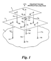
- a conducting ground plane 1 is provided and stacked above that are patches 2 and 3.
- the ground plane 1 co-operates with the patch 2 serving as a reflector against which the patch 2 is electrically driven.
- the patch 2 is resonant at a frequency in the lower operating frequency band, whilst the patch 3 is intended to resonant at a frequency in the upper frequency band and utilises the patch 2 as its ground plane.
- Each of the patches is spaced from its respective ground plane by less than a quarter of a wave length at the patch operating frequency and each is shaped so that it can operate in two mutually orthogonal modes and radiate respective orthogonal polarisations.
- the lower patch is driven from voltage sources 4a, 4b and 5a, 5b established on the ground plane 1 and connected to the patch 2 by means of probe wires 10a - 10d and series capacitors 8a - 8d formed within the patch.
- the upper patch 3 is driven by voltage sources 6a, 6b and 7a, 7b established in the lower frequency patch and connected by respective wire probes 11a - 11d and series capacitors 9a - 9d within the upper frequency patch.
- imaginary lines drawn between the diametrically opposed probes e.g. 10a, 10c and 10b, 10d are orthogonal and hence well isolated dual polarised radiation can be achieved.
- the probe ends within a diagonal set are placed on the voltage node line of the mode orthogonal to that set ensuring that the feed voltages at for example, 4a and 4b and 5a and 5b are equal and opposite in magnitude.
- the series capacitors, patch size and height and the length of cable between pairs of probes the antenna can be made to have a VSWR (Voltage Standing Wave Ratio) of less than 1.2:1 across each frequency band.
- VSWR Voltage Standing Wave Ratio
- the feed to a pair of voltage sources is arranged such that the feed is initially to a first of the pair and then by a delay cable from the first of the pair to the second. If the delay cable is selected to create a delay of half a wavelength, then the two associated probes can be fed 180° out of phase at the operating frequency of the patch.
- the upper frequency patch should be central with respect to the lower frequency patch and this should certainly be the best case for pattern symmetry.
- isolation between each band has been found to be adequate for the GSM and PCN bands. This is attributed to the fact that each patch is considerably off resonance with respect to the other.
- the resonance frequency of an upper patch in a pair is approximately at least twice the frequency of the resonance frequency of the lower one in a pair.
- the ground plane 1 and patches 2 and 3 are conveniently formed from squares of double sided printed circuit board, and for convenience, are spaced from each other by insulating pillars 13, 14.
- the patch 2 is fed via cables 4 and 5 and delay cables 12a, 12b, whilst patch 3 is similarly fed by cables 8 and 9 and corresponding delay cables 15a and 15b.
- the two sides of the double printed circuit 16 board forming the ground plane are electrically connected together so that even though the patch 2 extends slightly beyond the printed circuit board 16 it is electrically surrounded by the much larger ground plane 1. This ensures that the ground plane 1 does not resonate at the design resonant frequency of the patch 2 and reflects the radiation in the patch 2 away from the ground plane 1.
- top metallic layer 1a overlaps the hole 17 in the board 16 and is strongly capacitively coupled to ground via the intervening dielectric. This enables RF connection of the two sides which make up the ground plane 16 to ground without the usual metallic connection problems of dissimilar metal junctions.
- probes 10 and 11 are coupled into the patches by respective dielectric bushes, for example those shown at 8a - 8d, and these allow for a controlled capacitive coupling.
- the patch 3 is significantly smaller than the patch 2 and in any case should not extend beyond the ground plane constituted by the patch 2.
- the corners of the patch 3 are removed simply for assembly purposes and to all intents and purposes the patch 3 is effectively square.
Landscapes
- Physics & Mathematics (AREA)
- Electromagnetism (AREA)
- Waveguide Aerials (AREA)
- Variable-Direction Aerials And Aerial Arrays (AREA)
- Aerials With Secondary Devices (AREA)
Applications Claiming Priority (2)
| Application Number | Priority Date | Filing Date | Title |
|---|---|---|---|
| GB9916146A GB2352091B (en) | 1999-07-10 | 1999-07-10 | Patch antenna |
| GB9916146 | 1999-07-10 |
Publications (2)
| Publication Number | Publication Date |
|---|---|
| EP1069646A2 true EP1069646A2 (fr) | 2001-01-17 |
| EP1069646A3 EP1069646A3 (fr) | 2001-07-04 |
Family
ID=10856973
Family Applications (1)
| Application Number | Title | Priority Date | Filing Date |
|---|---|---|---|
| EP00305729A Ceased EP1069646A3 (fr) | 1999-07-10 | 2000-07-06 | Antenne à microbande |
Country Status (2)
| Country | Link |
|---|---|
| EP (1) | EP1069646A3 (fr) |
| GB (1) | GB2352091B (fr) |
Cited By (7)
| Publication number | Priority date | Publication date | Assignee | Title |
|---|---|---|---|---|
| WO2002050940A3 (fr) * | 2000-12-21 | 2002-08-29 | Kathrein Werke Kg | Antenne a plaque, conçue pour fonctionner dans au moins deux gammes de frequences |
| WO2004051798A1 (fr) * | 2002-12-02 | 2004-06-17 | Obschestvo S Ogranichennoy Otvetstvennostju 'algoritm' | Dispositif d'antenne a diagramme de directivite reglable et antenne planaire directionnelle |
| EP1531517A1 (fr) * | 2003-11-12 | 2005-05-18 | Alps Electric Co., Ltd. | Antenne haute fiabilité à polarisation circulaire en tole métallique |
| WO2006059937A1 (fr) * | 2004-11-30 | 2006-06-08 | Powerwave Technologies Sweden Ab | Descente d'antenne double bande |
| US7292201B2 (en) | 2005-08-22 | 2007-11-06 | Airgain, Inc. | Directional antenna system with multi-use elements |
| WO2014091458A3 (fr) * | 2012-12-13 | 2014-11-06 | Poynting Antennas (Pty) Limited | Agencement d'antennes à plaque à double polarisation |
| US11652301B2 (en) | 2018-04-11 | 2023-05-16 | Qualcomm Incorporated | Patch antenna array |
Family Cites Families (8)
| Publication number | Priority date | Publication date | Assignee | Title |
|---|---|---|---|---|
| US4660048A (en) * | 1984-12-18 | 1987-04-21 | Texas Instruments Incorporated | Microstrip patch antenna system |
| GB8501225D0 (en) * | 1985-01-17 | 1985-02-20 | Cossor Electronics Ltd | Antenna |
| US5003318A (en) * | 1986-11-24 | 1991-03-26 | Mcdonnell Douglas Corporation | Dual frequency microstrip patch antenna with capacitively coupled feed pins |
| US4947178A (en) * | 1988-05-02 | 1990-08-07 | Lotfollah Shafai | Scanning antenna |
| US5043738A (en) * | 1990-03-15 | 1991-08-27 | Hughes Aircraft Company | Plural frequency patch antenna assembly |
| US5153600A (en) * | 1991-07-01 | 1992-10-06 | Ball Corporation | Multiple-frequency stacked microstrip antenna |
| FR2709878B1 (fr) * | 1993-09-07 | 1995-11-24 | Univ Limoges | Antenne fil-plaque monopolaire. |
| US5880694A (en) * | 1997-06-18 | 1999-03-09 | Hughes Electronics Corporation | Planar low profile, wideband, wide-scan phased array antenna using a stacked-disc radiator |
-
1999
- 1999-07-10 GB GB9916146A patent/GB2352091B/en not_active Expired - Fee Related
-
2000
- 2000-07-06 EP EP00305729A patent/EP1069646A3/fr not_active Ceased
Non-Patent Citations (1)
| Title |
|---|
| None * |
Cited By (11)
| Publication number | Priority date | Publication date | Assignee | Title |
|---|---|---|---|---|
| WO2002050940A3 (fr) * | 2000-12-21 | 2002-08-29 | Kathrein Werke Kg | Antenne a plaque, conçue pour fonctionner dans au moins deux gammes de frequences |
| US6861988B2 (en) | 2000-12-21 | 2005-03-01 | Kathrein-Werke Kg | Patch antenna for operating in at least two frequency ranges |
| WO2004051798A1 (fr) * | 2002-12-02 | 2004-06-17 | Obschestvo S Ogranichennoy Otvetstvennostju 'algoritm' | Dispositif d'antenne a diagramme de directivite reglable et antenne planaire directionnelle |
| EP1531517A1 (fr) * | 2003-11-12 | 2005-05-18 | Alps Electric Co., Ltd. | Antenne haute fiabilité à polarisation circulaire en tole métallique |
| US7075486B2 (en) | 2003-11-12 | 2006-07-11 | Alps Electric Co., Ltd. | Circularly polarized wave antenna made of sheet metal with high reliability |
| WO2006059937A1 (fr) * | 2004-11-30 | 2006-06-08 | Powerwave Technologies Sweden Ab | Descente d'antenne double bande |
| US7292201B2 (en) | 2005-08-22 | 2007-11-06 | Airgain, Inc. | Directional antenna system with multi-use elements |
| WO2014091458A3 (fr) * | 2012-12-13 | 2014-11-06 | Poynting Antennas (Pty) Limited | Agencement d'antennes à plaque à double polarisation |
| US11652301B2 (en) | 2018-04-11 | 2023-05-16 | Qualcomm Incorporated | Patch antenna array |
| EP3776735B1 (fr) * | 2018-04-11 | 2024-07-17 | QUALCOMM Incorporated | Réseau d'antennes à plaque |
| US12136766B2 (en) | 2018-04-11 | 2024-11-05 | Qualcomm Incorporated | Patch antenna array |
Also Published As
| Publication number | Publication date |
|---|---|
| GB9916146D0 (en) | 1999-09-08 |
| EP1069646A3 (fr) | 2001-07-04 |
| GB2352091A (en) | 2001-01-17 |
| GB2352091B (en) | 2003-09-17 |
Similar Documents
| Publication | Publication Date | Title |
|---|---|---|
| US11777229B2 (en) | Antennas including multi-resonance cross-dipole radiating elements and related radiating elements | |
| US6317099B1 (en) | Folded dipole antenna | |
| US6734828B2 (en) | Dual band planar high-frequency antenna | |
| AU724045B2 (en) | Antenna mutual coupling neutralizer | |
| EP1118138B1 (fr) | Antenne resonante dielectrique a polarisation circulaire | |
| KR100997895B1 (ko) | 2중-피드, 다중-대역, 평면 안테나 | |
| US7015868B2 (en) | Multilevel Antennae | |
| US6509882B2 (en) | Low SAR broadband antenna assembly | |
| EP3813192B1 (fr) | Élément rayonnant à double polarisation et bande ultra large pour antenne de station de base | |
| AU778969B2 (en) | Folded dipole antenna | |
| US20110001682A1 (en) | Compact single feed dual-polarized dual-frequency band microstrip antenna array | |
| US20040145526A1 (en) | Dual-band dual-polarized antenna array | |
| US20030103015A1 (en) | Skeleton slot radiation element and multi-band patch antenna using the same | |
| JP2003258540A (ja) | 積層パッチアンテナ組立体 | |
| KR100616545B1 (ko) | 이중 커플링 급전을 이용한 다중밴드용 적층형 칩 안테나 | |
| EP3387706B1 (fr) | Antenne et élément rayonnant pour antenne | |
| JP2003514422A (ja) | プリントアンテナ | |
| US12512606B2 (en) | Multiband cross-dipole radiating elements and base station antennas including arrays of such radiating elements | |
| JPH11150415A (ja) | 多周波アンテナ | |
| US6885343B2 (en) | Stripline parallel-series-fed proximity-coupled cavity backed patch antenna array | |
| US11264730B2 (en) | Quad-port radiating element | |
| US6956533B2 (en) | Antenna having a monopole design, for use in several wireless communication services | |
| KR101992620B1 (ko) | 고이득 전방향성 안테나 | |
| US20030103008A1 (en) | In-building low profile antenna | |
| EP1069646A2 (fr) | Antenne à microbande |
Legal Events
| Date | Code | Title | Description |
|---|---|---|---|
| PUAI | Public reference made under article 153(3) epc to a published international application that has entered the european phase |
Free format text: ORIGINAL CODE: 0009012 |
|
| AK | Designated contracting states |
Kind code of ref document: A2 Designated state(s): AT BE CH CY DE DK ES FI FR GB GR IE IT LI LU MC NL PT SE |
|
| AX | Request for extension of the european patent |
Free format text: AL;LT;LV;MK;RO;SI |
|
| PUAL | Search report despatched |
Free format text: ORIGINAL CODE: 0009013 |
|
| AK | Designated contracting states |
Kind code of ref document: A3 Designated state(s): AT BE CH CY DE DK ES FI FR GB GR IE IT LI LU MC NL PT SE |
|
| AX | Request for extension of the european patent |
Free format text: AL;LT;LV;MK;RO;SI |
|
| 17P | Request for examination filed |
Effective date: 20011227 |
|
| AKX | Designation fees paid |
Free format text: AT BE CH CY DE DK ES FI FR GB GR IE IT LI LU MC NL PT SE |
|
| RBV | Designated contracting states (corrected) |
Designated state(s): AT BE CH CY DE DK ES FI FR GR IE IT LI LU MC NL PT SE |
|
| 17Q | First examination report despatched |
Effective date: 20040906 |
|
| STAA | Information on the status of an ep patent application or granted ep patent |
Free format text: STATUS: THE APPLICATION HAS BEEN REFUSED |
|
| 18R | Application refused |
Effective date: 20061112 |
|
| REG | Reference to a national code |
Ref country code: HK Ref legal event code: WD Ref document number: 1035265 Country of ref document: HK |