EP1069644A2 - Antenna assembly - Google Patents
Antenna assembly Download PDFInfo
- Publication number
- EP1069644A2 EP1069644A2 EP00114186A EP00114186A EP1069644A2 EP 1069644 A2 EP1069644 A2 EP 1069644A2 EP 00114186 A EP00114186 A EP 00114186A EP 00114186 A EP00114186 A EP 00114186A EP 1069644 A2 EP1069644 A2 EP 1069644A2
- Authority
- EP
- European Patent Office
- Prior art keywords
- antenna assembly
- hexahedron
- convex portions
- conductive film
- pattern
- Prior art date
- Legal status (The legal status is an assumption and is not a legal conclusion. Google has not performed a legal analysis and makes no representation as to the accuracy of the status listed.)
- Granted
Links
Images

Classifications
-
- H—ELECTRICITY
- H01—ELECTRIC ELEMENTS
- H01Q—ANTENNAS, i.e. RADIO AERIALS
- H01Q1/00—Details of, or arrangements associated with, antennas
- H01Q1/12—Supports; Mounting means
- H01Q1/22—Supports; Mounting means by structural association with other equipment or articles
- H01Q1/24—Supports; Mounting means by structural association with other equipment or articles with receiving set
- H01Q1/241—Supports; Mounting means by structural association with other equipment or articles with receiving set used in mobile communications, e.g. GSM
- H01Q1/242—Supports; Mounting means by structural association with other equipment or articles with receiving set used in mobile communications, e.g. GSM specially adapted for hand-held use
- H01Q1/243—Supports; Mounting means by structural association with other equipment or articles with receiving set used in mobile communications, e.g. GSM specially adapted for hand-held use with built-in antennas
-
- H—ELECTRICITY
- H01—ELECTRIC ELEMENTS
- H01Q—ANTENNAS, i.e. RADIO AERIALS
- H01Q1/00—Details of, or arrangements associated with, antennas
-
- H—ELECTRICITY
- H01—ELECTRIC ELEMENTS
- H01Q—ANTENNAS, i.e. RADIO AERIALS
- H01Q1/00—Details of, or arrangements associated with, antennas
- H01Q1/36—Structural form of radiating elements, e.g. cone, spiral, umbrella; Particular materials used therewith
- H01Q1/38—Structural form of radiating elements, e.g. cone, spiral, umbrella; Particular materials used therewith formed by a conductive layer on an insulating support
-
- H—ELECTRICITY
- H01—ELECTRIC ELEMENTS
- H01Q—ANTENNAS, i.e. RADIO AERIALS
- H01Q9/00—Electrically-short antennas having dimensions not more than twice the operating wavelength and consisting of conductive active radiating elements
- H01Q9/04—Resonant antennas
- H01Q9/0407—Substantially flat resonant element parallel to ground plane, e.g. patch antenna
- H01Q9/0421—Substantially flat resonant element parallel to ground plane, e.g. patch antenna with a shorting wall or a shorting pin at one end of the element
-
- Y—GENERAL TAGGING OF NEW TECHNOLOGICAL DEVELOPMENTS; GENERAL TAGGING OF CROSS-SECTIONAL TECHNOLOGIES SPANNING OVER SEVERAL SECTIONS OF THE IPC; TECHNICAL SUBJECTS COVERED BY FORMER USPC CROSS-REFERENCE ART COLLECTIONS [XRACs] AND DIGESTS
- Y10—TECHNICAL SUBJECTS COVERED BY FORMER USPC
- Y10T—TECHNICAL SUBJECTS COVERED BY FORMER US CLASSIFICATION
- Y10T29/00—Metal working
- Y10T29/49—Method of mechanical manufacture
- Y10T29/49002—Electrical device making
- Y10T29/49016—Antenna or wave energy "plumbing" making
Definitions
- the present invention relates to an antenna assembly comprising a hexahedron of a dielectric material on the surface of which a patterned conductive film is formed.
- the main body of this antenna is assembled so that a desired pattern of a conductive film is formed on each surface of a hexahedron of a dielectric material.
- the conductive film has been formed either by printing, plating, vapor deposition or sputtering.
- the method for forming the conductive film either by plating, vapor deposition or sputtering comprises: a lift-off method in which the conductive film is formed after forming a resist film on the area where the conductive film is not formed on each face, followed by removing the resist film; and an etching method in which, after forming a conductive film on the entire surfaces on which the pattern is to be formed, a pattern of a resist film is formed on the foregoing film, followed by removing the conductive film in the area not covered with the resist film by etching.
- the object of the present invention in view of the problems as set forth above is to provide a cheap antenna assembly suitable for mass-production, wherein a patterned conductive film is formed on the surface of a dielectric hexahedron.
- the present invention for solving the foregoing problems provided an antenna assembly comprising a hexahedron of a dielectric material on each surface of which convex portions to serve as a circuit pattern are formed, wherein the circuit pattern comprising a conductive film is only formed on the convex portions.
- the present invention provides a method for manufacturing an antenna assembly, wherein concave and convex portions are machined on the surface of a hexahedron of a dielectric material, and a desired pattern of a conductive film is formed on the convex portions using a roll coater.
- hexahedron denotes not only a cube or a rectangular parallelpiped column, but also any type of hexahedrons so far as they have six faces. However, any of the two faces among the six faces are preferably in a parallel relation one another in view of the spirit of the present invention.
- Such hexahedrons having concave and convex portions formed on the surfaces of a hexahedron such as a cube or a rectangular parallelpiped column, or those having hollow spaces also belong to the hexahedron according to the present invention.
- the dielectric material constituting the hexahedron desirably comprises a ceramic, glass or a mixture of a ceramic and glass in view of mechanical strength
- any dielectric materials may be used so long as it is not contrary to the spirit of the present invention. Accordingly, plastics are acceptable for that purpose.
- a film comprising a pure metal or metal alloy may be advantageously used as the conductive film, use of other conductive materials such as a conductive resin is also possible.
- the edge angle between the surface of the hexahedron and the inner wall of the concave portion is 80 degree or more and 135 degree or less.
- the edge may be chipped on the edge when the angle is less than 80 degree while, when the angle is larger than 135 degree, inner faces of the concave portion may be contaminated during deposition of the conductive film to compromise the function of the antenna.
- a edge angle of more than 90 degree and less than 120 degree is desirable when the function of the antenna is emphasized.
- the conductive film should be continuously formed through the mutually adjoining faces on the hexahedron in the present invention, and the edges are desirably chamfered, because the conductive film formed by coating a conductive paste may be possibly interrupted at the edge when the edges are not chamfered.
- the radius of chamfering is desirably 0.1 mm or more and 0.5 mm or less. The effect of chamfering will be invalid when the radius of chamfering is less than 0.1 mm, while the conductive paste can be hardly spread on the chamfered edge during coating to rather interrupt the conductive film when the radius of chamfering is larger than 0.5 mm.
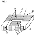
- FIG. 1 shows a perspective view representing one embodiment of the antenna assembly according to the present invention.
- the pattern of the conductive film shown in FIG. 1 is merely one example among existing various patterns, and the present invention is never restricted to the pattern as set forth herein.
- the conductive film may be also formed on the remaining faces on which the conductive films have not been formed yet, or on the faces having no concave and convex portions, after forming the convex and concave portions.
- the antenna assembly 10 is a hexahedron on the four surfaces 11 , 12 , 13 , and 14 of which concave and convex portions are formed.
- Conductive films 30 are formed on the convex portions on the four surfaces 11 , 12 , 13 , and 14 .
- the dielectric material in this embodiment comprises a mixture of a ceramic and glass, and the conductive films 30 comprise an Ag/Pd film.
- the surface 12 shown in FIG. 1 serves as an emission pattern face of the antenna, and the surface 13 serves as a power feed pattern face of the antenna.
- a Short-circuit pattern face and grounding face of the antenna are formed as well on the surfaces 11 and 14 , respectively, although they are not illustrated.
- Concave portions with a depth of 200 ⁇ m are formed on the area not indicated by the dotted lines in this perspective view. Since the Ag/Pd film is not deposited on the concave portions, a prescribed pattern that functions as an antenna is formed on the antenna assembly 10 . No machining is applied on the remaining faces of the hexahedron in this embodiment.
- a mixture of an alumina powder, and two kinds of glass powders of CaO-Al 2 O 3 -SiO 2 based and PbO-BaO-SiO 2 based glasses are firstly prepared as a starting material of the dielectric material.
- the mixed powder is kneaded and granulated after adding water, an organic binder and a surface active agent.
- the granules are subjected to a press molding that also serves for forming concave and convex portions, thereby manufacturing hexahedrons, or rectangular parallelpiped columns, on the surfaces of which a pattern of the concave and convex portions are formed.
- the hexahedron is fired to manufacture a hexahedron of a dielectric material.
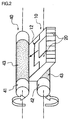
- conductive films are formed on the four faces 11 , 12 , 13 , and 14 of the fired hexahedron using a roll coater shown in FIG. 2.
- FIG. 2 shows a schematic drawing of the method for forming the conductive film using the roll coater in FIG. 2.
- the roll coater has a pair of rolls 41 and 42 rotating along the opposite directions with each other, and an Ag/Pd paste is coated on the rolls 41 and 42 .
- an antenna assembly 10 on the surface of which convex portions 20 are formed are inserted between two rollers so that the surfaces 12 and 14 make slight contact with either the roller 41 or the roller 42 . Since the Ag/Pd paste only adheres on the convex portions after printing with the roll coater 40 , the Ag/Pd films comprising a pattern of the emission face and a pattern of the grounding face of the antenna assembly are formed on the surface 12 and on the back face 14 .
- the antenna assembly 10 is inserted between the rollers of the roll coater 40 by allowing the insertion angle of the antenna assembly 10 relative to the roll coater 40 to rotate by an angle of 90 degree, to simultaneously print the short-circuit pattern face and the power feed pattern face of the antenna on the surfaces 11 and 13 , respectively, thereby obtaining the antenna assembly on the four surfaces 11 , 12 , 13 , and 14 of which the Ag/Pd films with desired patterns are formed.
- a plurality of the antenna assemblies may be simultaneously manufactured in this embodiment by simultaneously inserting a plurality of antennae between the rollers of the roll coater.
- An antenna assembly fired by the same method as described above is also prepared in the method for forming the conductive film in this embodiment. While the roll coater 40 having the same feature as described above (see FIG. 2) is also used in this embodiment, a solution of palladium chloride is coated on the roll coater in this method.
- the antenna assembly 10 coated with an aqueous solution of palladium chloride on its convex portions is dipped in a nickel electroless plating bath (not shown) in the next step to apply nickel plating on the portions where palladium chloride has been coated. In other words the conductive films are formed on the convex portions.
- FIGS. 3A to 3D denote expanded drawings of the assembly manufactured In the third embodiment of the method for manufacturing the antenna assembly according to the present invention.
- FIGS. 3A to 3D The expanded drawings of the assembly manufactured in the third embodiment of the method for manufacturing the assembly 50 according to the present invention are illustrated in FIGS. 3A to 3D.
- the assembly 50 comprises a hexahedron of a ceramic, wherein concave portions 60 (the portions not indicated by the dotted lines) with a width of 200 ⁇ m and a depth of 400 ⁇ m are formed on the surface 52 among the four surfaces 51 , 52 , 53 , and 54 .
- An aluminum film 70 (the portions indicated by the dotted lines) that is a different material from the constituting material of the assembly 50 is formed on the portions of the surface 52 excluding the concave portion 60 .
- the surface 52 shown in FIG. 3B corresponds to a top face of the assembly 50
- the surface 54 shown in FIG. 3D denotes a bottom face.
- a plurality of these assemblies were arranged along the horizontal direction with the surface 52 as the top face upward, and the Al film was formed by sputtering on the five surfaces of each assembly except the surface 54 as a bottom face.
- the Al film was adhered on a part of the inner wall face of the concave portion, no film adhered on the wall face at a depth of 200 ⁇ m or more, indicating that patterned films can be formed on the surface of the polyhedron by the method for manufacturing the assembly according to the present invention.
- Such assembly as described above can be machined to utilized it as an antenna assembly.
- the same result as described in the third embodiment can be also obtained when the Al film is deposited by using a vapor deposition method, instead of the sputtering method used in the third embodiment.
- the conductive films are formed only on the convex portions of the hexahedron of the dielectric material on the surface of which the concave and convex portions are formed in the antenna assembly according to the present invention. Consequently, the conductive films that are essential for the antenna assembly can be precisely and easily deposited to enable the good quality antenna assembly to be cheaply manufactured in large scale.
Landscapes
- Engineering & Computer Science (AREA)
- Computer Networks & Wireless Communication (AREA)
- Details Of Aerials (AREA)
Abstract
Description
Claims (2)
- An antenna assembly 10 comprising a hexahedron on each surface of which convex portions to serve as a circuit pattern are formed, characterized in that the circuit pattern comprising a conductive film 30 is formed only on the convex portions.
- A method for manufacturing an antenna assembly 10, characterized in that concave and convex portions are machined on the surface of a hexahedron of a dielectric material, and a desired pattern of a conductive film 30 is formed on the convex portions using a roll coater.
Applications Claiming Priority (2)
| Application Number | Priority Date | Filing Date | Title |
|---|---|---|---|
| JP20281899A JP2000228603A (en) | 1998-12-01 | 1999-07-16 | Antenna structure |
| JP20281899 | 1999-07-16 |
Publications (3)
| Publication Number | Publication Date |
|---|---|
| EP1069644A2 true EP1069644A2 (en) | 2001-01-17 |
| EP1069644A3 EP1069644A3 (en) | 2002-05-02 |
| EP1069644B1 EP1069644B1 (en) | 2008-01-02 |
Family
ID=16463716
Family Applications (1)
| Application Number | Title | Priority Date | Filing Date |
|---|---|---|---|
| EP00114186A Expired - Lifetime EP1069644B1 (en) | 1999-07-16 | 2000-07-13 | Antenna assembly |
Country Status (5)
| Country | Link |
|---|---|
| US (1) | US6531983B1 (en) |
| EP (1) | EP1069644B1 (en) |
| KR (1) | KR100702089B1 (en) |
| DE (1) | DE60037620T2 (en) |
| TW (1) | TW497249B (en) |
Families Citing this family (16)
| Publication number | Priority date | Publication date | Assignee | Title |
|---|---|---|---|---|
| US7006050B2 (en) * | 2001-02-15 | 2006-02-28 | Integral Technologies, Inc. | Low cost antennas manufactured from conductive loaded resin-based materials having a conducting wire center core |
| US6947005B2 (en) * | 2001-02-15 | 2005-09-20 | Integral Technologies, Inc. | Low cost antennas and electromagnetic (EMF) absorption in electronic circuit packages or transceivers using conductive loaded resin-based materials |
| CN100454661C (en) * | 2001-07-31 | 2009-01-21 | 日立麦克赛尔株式会社 | Planar antenna and manufacturing method thereof |
| US6873298B1 (en) | 2002-09-25 | 2005-03-29 | Integral Technologies, Inc. | Plastenna flat panel antenna |
| KR100781667B1 (en) * | 2005-03-31 | 2007-12-04 | 엘지전자 주식회사 | Mobile communication terminal |
| USD534544S1 (en) * | 2005-04-22 | 2007-01-02 | Microsoft Corporation | Icon for a portion of a display screen |
| US7642918B2 (en) * | 2005-10-21 | 2010-01-05 | Georgia Tech Research Corporation | Thin flexible radio frequency identification tags and subsystems thereof |
| KR100881120B1 (en) | 2007-04-10 | 2009-02-11 | 주식회사 광현에어텍 | Cellular Intenna and Manufacturing Method |
| JP4788791B2 (en) * | 2009-02-27 | 2011-10-05 | Tdk株式会社 | Antenna device |
| JP2012525065A (en) * | 2009-04-21 | 2012-10-18 | モレックス インコーポレイテド | 3D antenna |
| US8745853B2 (en) * | 2010-07-05 | 2014-06-10 | Universal Display Corporation | Antenna fabrication with three-dimensional contoured substrates |
| TWI508366B (en) * | 2011-06-20 | 2015-11-11 | Jieng Tai Internat Electric Corp | Method of forming antenna |
| JP5914142B2 (en) | 2011-09-14 | 2016-05-11 | タイコエレクトロニクスジャパン合同会社 | Conductive member and conductive member assembly |
| USD768115S1 (en) * | 2015-02-05 | 2016-10-04 | Armen E. Kazanchian | Module |
| US9914184B2 (en) | 2015-10-02 | 2018-03-13 | Te Connectivity Corporation | 3D formed LDS liner and method of manufacturing liner |
| KR101782950B1 (en) * | 2016-04-19 | 2017-09-28 | (주)파트론 | Antenna structure |
Family Cites Families (9)
| Publication number | Priority date | Publication date | Assignee | Title |
|---|---|---|---|---|
| US4677404A (en) * | 1984-12-19 | 1987-06-30 | Martin Marietta Corporation | Compound dielectric multi-conductor transmission line |
| DE3732986C2 (en) * | 1987-09-30 | 1997-12-18 | Daimler Benz Aerospace Ag | Group antenna with patch radiating elements |
| CA2070204A1 (en) * | 1992-06-02 | 1993-12-03 | Nobuo Shiga | Receiver device |
| CN1094663C (en) * | 1994-03-08 | 2002-11-20 | 泰利泰尔有限责任公司 | Hand-held transmitting and/or receiving apparatus |
| US5815122A (en) * | 1996-01-11 | 1998-09-29 | The Regents Of The University Of Michigan | Slot spiral antenna with integrated balun and feed |
| TW356610B (en) * | 1996-02-19 | 1999-04-21 | Murata Mfg Corp | Antenna apparatus and communication apparatus using the same |
| US6060121A (en) * | 1996-03-15 | 2000-05-09 | President And Fellows Of Harvard College | Microcontact printing of catalytic colloids |
| JPH10125820A (en) * | 1996-10-18 | 1998-05-15 | Sumitomo Metal Ind Ltd | Ceramic circuit board and method of manufacturing the same |
| EP1028483B1 (en) * | 1999-02-10 | 2006-09-27 | AMC Centurion AB | Method and device for manufacturing a roll of antenna elements and for dispensing said antenna elements |
-
2000
- 2000-07-13 DE DE60037620T patent/DE60037620T2/en not_active Expired - Lifetime
- 2000-07-13 EP EP00114186A patent/EP1069644B1/en not_active Expired - Lifetime
- 2000-07-14 TW TW089114138A patent/TW497249B/en not_active IP Right Cessation
- 2000-07-14 KR KR1020000040468A patent/KR100702089B1/en not_active Expired - Lifetime
- 2000-07-17 US US09/618,062 patent/US6531983B1/en not_active Expired - Lifetime
Also Published As
| Publication number | Publication date |
|---|---|
| KR20010021083A (en) | 2001-03-15 |
| US6531983B1 (en) | 2003-03-11 |
| KR100702089B1 (en) | 2007-04-02 |
| EP1069644B1 (en) | 2008-01-02 |
| TW497249B (en) | 2002-08-01 |
| DE60037620D1 (en) | 2008-02-14 |
| EP1069644A3 (en) | 2002-05-02 |
| DE60037620T2 (en) | 2008-12-24 |
Similar Documents
| Publication | Publication Date | Title |
|---|---|---|
| EP1069644A2 (en) | Antenna assembly | |
| US6576497B2 (en) | Chip-type electronic component | |
| US7796087B2 (en) | Antenna apparatus having a ground plate and feeding unit | |
| EP1042079A1 (en) | Improved miniature surface mount capacitor and method of making same | |
| EP0971379B1 (en) | Inductor device and process of production thereof | |
| JPS6356942A (en) | Work holder | |
| CN1204651C (en) | Central electrode subassembly and its production method, nonreciprocal circuit device, communication device | |
| CN101257140A (en) | Method for manufacturing antenna module by laser engraving | |
| JP2000228603A (en) | Antenna structure | |
| EP1122810B1 (en) | Antenna device | |
| US20090322468A1 (en) | Chip Resistor and Manufacturing Method Thereof | |
| CN214226651U (en) | Array type chip resistor | |
| CN215266659U (en) | Plastic metallized vibrator unit and communication equipment | |
| JPH06204100A (en) | Mask jig for forming external electrode of chip-shape circuit component | |
| JPH10189305A (en) | Angular plate type chip resistor and its manufacture | |
| WO2022105378A1 (en) | Glass plate, manufacturing method, housing, and electronic device | |
| JPH05175719A (en) | Microstrip antenna manufacturing method and resonance frequency adjusting method | |
| JP3493958B2 (en) | Coaxial dielectric resonator and method of manufacturing the same | |
| JPH01264805A (en) | Manufacture of ceramic substrate | |
| SU815979A1 (en) | Printed circuit board manufacturing method | |
| JPH11176603A (en) | Chip resistor | |
| CN110690567B (en) | Fractal monopole array ultra-wideband positioning beacon antenna | |
| JPH0144032B2 (en) | ||
| JPH0218080A (en) | Printing on three-dimensional surface | |
| CN120810252A (en) | Manufacturing method of antenna assembly, antenna module and communication equipment |
Legal Events
| Date | Code | Title | Description |
|---|---|---|---|
| PUAI | Public reference made under article 153(3) epc to a published international application that has entered the european phase |
Free format text: ORIGINAL CODE: 0009012 |
|
| AK | Designated contracting states |
Kind code of ref document: A2 Designated state(s): DE FI GB SE Kind code of ref document: A2 Designated state(s): AT BE CH CY DE DK ES FI FR GB GR IE IT LI LU MC NL PT SE |
|
| AX | Request for extension of the european patent |
Free format text: AL;LT;LV;MK;RO;SI |
|
| PUAL | Search report despatched |
Free format text: ORIGINAL CODE: 0009013 |
|
| AK | Designated contracting states |
Kind code of ref document: A3 Designated state(s): AT BE CH CY DE DK ES FI FR GB GR IE IT LI LU MC NL PT SE |
|
| AX | Request for extension of the european patent |
Free format text: AL;LT;LV;MK;RO;SI |
|
| 17P | Request for examination filed |
Effective date: 20020911 |
|
| AKX | Designation fees paid |
Free format text: DE FI GB SE |
|
| 17Q | First examination report despatched |
Effective date: 20031028 |
|
| 17Q | First examination report despatched |
Effective date: 20031028 |
|
| GRAP | Despatch of communication of intention to grant a patent |
Free format text: ORIGINAL CODE: EPIDOSNIGR1 |
|
| GRAS | Grant fee paid |
Free format text: ORIGINAL CODE: EPIDOSNIGR3 |
|
| GRAA | (expected) grant |
Free format text: ORIGINAL CODE: 0009210 |
|
| AK | Designated contracting states |
Kind code of ref document: B1 Designated state(s): DE FI GB SE |
|
| REG | Reference to a national code |
Ref country code: GB Ref legal event code: FG4D |
|
| REF | Corresponds to: |
Ref document number: 60037620 Country of ref document: DE Date of ref document: 20080214 Kind code of ref document: P |
|
| REG | Reference to a national code |
Ref country code: SE Ref legal event code: TRGR |
|
| PLBE | No opposition filed within time limit |
Free format text: ORIGINAL CODE: 0009261 |
|
| STAA | Information on the status of an ep patent application or granted ep patent |
Free format text: STATUS: NO OPPOSITION FILED WITHIN TIME LIMIT |
|
| 26N | No opposition filed |
Effective date: 20081003 |
|
| PGFP | Annual fee paid to national office [announced via postgrant information from national office to epo] |
Ref country code: FI Payment date: 20190722 Year of fee payment: 20 Ref country code: DE Payment date: 20190719 Year of fee payment: 20 Ref country code: SE Payment date: 20190719 Year of fee payment: 20 |
|
| PGFP | Annual fee paid to national office [announced via postgrant information from national office to epo] |
Ref country code: GB Payment date: 20190719 Year of fee payment: 20 |
|
| REG | Reference to a national code |
Ref country code: DE Ref legal event code: R071 Ref document number: 60037620 Country of ref document: DE |
|
| REG | Reference to a national code |
Ref country code: GB Ref legal event code: PE20 Expiry date: 20200712 |
|
| REG | Reference to a national code |
Ref country code: FI Ref legal event code: MAE |
|
| REG | Reference to a national code |
Ref country code: SE Ref legal event code: EUG |
|
| REG | Reference to a national code |
Ref country code: SE Ref legal event code: EUG |
|
| PG25 | Lapsed in a contracting state [announced via postgrant information from national office to epo] |
Ref country code: GB Free format text: LAPSE BECAUSE OF EXPIRATION OF PROTECTION Effective date: 20200712 |