EP1069617A2 - Multilayer wiring board - Google Patents
Multilayer wiring board Download PDFInfo
- Publication number
- EP1069617A2 EP1069617A2 EP00114903A EP00114903A EP1069617A2 EP 1069617 A2 EP1069617 A2 EP 1069617A2 EP 00114903 A EP00114903 A EP 00114903A EP 00114903 A EP00114903 A EP 00114903A EP 1069617 A2 EP1069617 A2 EP 1069617A2
- Authority
- EP
- European Patent Office
- Prior art keywords
- power
- layer
- source
- wiring
- conductive pattern
- Prior art date
- Legal status (The legal status is an assumption and is not a legal conclusion. Google has not performed a legal analysis and makes no representation as to the accuracy of the status listed.)
- Withdrawn
Links
Images








Classifications
-
- H—ELECTRICITY
- H05—ELECTRIC TECHNIQUES NOT OTHERWISE PROVIDED FOR
- H05K—PRINTED CIRCUITS; CASINGS OR CONSTRUCTIONAL DETAILS OF ELECTRIC APPARATUS; MANUFACTURE OF ASSEMBLAGES OF ELECTRICAL COMPONENTS
- H05K1/00—Printed circuits
- H05K1/02—Details
- H05K1/11—Printed elements for providing electric connections to or between printed circuits
- H05K1/111—Pads for surface mounting, e.g. lay-out
- H05K1/112—Pads for surface mounting, e.g. lay-out directly combined with via connections
- H05K1/114—Pad being close to via, but not surrounding the via
-
- H—ELECTRICITY
- H10—SEMICONDUCTOR DEVICES; ELECTRIC SOLID-STATE DEVICES NOT OTHERWISE PROVIDED FOR
- H10W—GENERIC PACKAGES, INTERCONNECTIONS, CONNECTORS OR OTHER CONSTRUCTIONAL DETAILS OF DEVICES COVERED BY CLASS H10
- H10W70/00—Package substrates; Interposers; Redistribution layers [RDL]
- H10W70/60—Insulating or insulated package substrates; Interposers; Redistribution layers
- H10W70/611—Insulating or insulated package substrates; Interposers; Redistribution layers for connecting multiple chips together
-
- H—ELECTRICITY
- H10—SEMICONDUCTOR DEVICES; ELECTRIC SOLID-STATE DEVICES NOT OTHERWISE PROVIDED FOR
- H10W—GENERIC PACKAGES, INTERCONNECTIONS, CONNECTORS OR OTHER CONSTRUCTIONAL DETAILS OF DEVICES COVERED BY CLASS H10
- H10W70/00—Package substrates; Interposers; Redistribution layers [RDL]
- H10W70/60—Insulating or insulated package substrates; Interposers; Redistribution layers
- H10W70/62—Insulating or insulated package substrates; Interposers; Redistribution layers characterised by their interconnections
- H10W70/63—Vias, e.g. via plugs
- H10W70/635—Through-vias
-
- H—ELECTRICITY
- H10—SEMICONDUCTOR DEVICES; ELECTRIC SOLID-STATE DEVICES NOT OTHERWISE PROVIDED FOR
- H10W—GENERIC PACKAGES, INTERCONNECTIONS, CONNECTORS OR OTHER CONSTRUCTIONAL DETAILS OF DEVICES COVERED BY CLASS H10
- H10W70/00—Package substrates; Interposers; Redistribution layers [RDL]
- H10W70/60—Insulating or insulated package substrates; Interposers; Redistribution layers
- H10W70/62—Insulating or insulated package substrates; Interposers; Redistribution layers characterised by their interconnections
- H10W70/65—Shapes or dispositions of interconnections
-
- H—ELECTRICITY
- H05—ELECTRIC TECHNIQUES NOT OTHERWISE PROVIDED FOR
- H05K—PRINTED CIRCUITS; CASINGS OR CONSTRUCTIONAL DETAILS OF ELECTRIC APPARATUS; MANUFACTURE OF ASSEMBLAGES OF ELECTRICAL COMPONENTS
- H05K1/00—Printed circuits
- H05K1/02—Details
- H05K1/0286—Programmable, customizable or modifiable circuits
- H05K1/0287—Programmable, customizable or modifiable circuits having an universal lay-out, e.g. pad or land grid patterns or mesh patterns
- H05K1/0289—Programmable, customizable or modifiable circuits having an universal lay-out, e.g. pad or land grid patterns or mesh patterns having a matrix lay-out, i.e. having selectively interconnectable sets of X-conductors and Y-conductors in different planes
-
- H—ELECTRICITY
- H05—ELECTRIC TECHNIQUES NOT OTHERWISE PROVIDED FOR
- H05K—PRINTED CIRCUITS; CASINGS OR CONSTRUCTIONAL DETAILS OF ELECTRIC APPARATUS; MANUFACTURE OF ASSEMBLAGES OF ELECTRICAL COMPONENTS
- H05K1/00—Printed circuits
- H05K1/02—Details
- H05K1/11—Printed elements for providing electric connections to or between printed circuits
- H05K1/115—Via connections; Lands around holes or via connections
-
- H—ELECTRICITY
- H05—ELECTRIC TECHNIQUES NOT OTHERWISE PROVIDED FOR
- H05K—PRINTED CIRCUITS; CASINGS OR CONSTRUCTIONAL DETAILS OF ELECTRIC APPARATUS; MANUFACTURE OF ASSEMBLAGES OF ELECTRICAL COMPONENTS
- H05K2201/00—Indexing scheme relating to printed circuits covered by H05K1/00
- H05K2201/09—Shape and layout
- H05K2201/09209—Shape and layout details of conductors
- H05K2201/095—Conductive through-holes or vias
- H05K2201/09627—Special connections between adjacent vias, not for grounding vias
-
- H—ELECTRICITY
- H05—ELECTRIC TECHNIQUES NOT OTHERWISE PROVIDED FOR
- H05K—PRINTED CIRCUITS; CASINGS OR CONSTRUCTIONAL DETAILS OF ELECTRIC APPARATUS; MANUFACTURE OF ASSEMBLAGES OF ELECTRICAL COMPONENTS
- H05K2201/00—Indexing scheme relating to printed circuits covered by H05K1/00
- H05K2201/09—Shape and layout
- H05K2201/09209—Shape and layout details of conductors
- H05K2201/09654—Shape and layout details of conductors covering at least two types of conductors provided for in H05K2201/09218 - H05K2201/095
- H05K2201/09709—Staggered pads, lands or terminals; Parallel conductors in different planes
-
- H—ELECTRICITY
- H05—ELECTRIC TECHNIQUES NOT OTHERWISE PROVIDED FOR
- H05K—PRINTED CIRCUITS; CASINGS OR CONSTRUCTIONAL DETAILS OF ELECTRIC APPARATUS; MANUFACTURE OF ASSEMBLAGES OF ELECTRICAL COMPONENTS
- H05K2201/00—Indexing scheme relating to printed circuits covered by H05K1/00
- H05K2201/09—Shape and layout
- H05K2201/09818—Shape or layout details not covered by a single group of H05K2201/09009 - H05K2201/09809
- H05K2201/09854—Hole or via having special cross-section, e.g. elliptical
-
- H—ELECTRICITY
- H05—ELECTRIC TECHNIQUES NOT OTHERWISE PROVIDED FOR
- H05K—PRINTED CIRCUITS; CASINGS OR CONSTRUCTIONAL DETAILS OF ELECTRIC APPARATUS; MANUFACTURE OF ASSEMBLAGES OF ELECTRICAL COMPONENTS
- H05K2201/00—Indexing scheme relating to printed circuits covered by H05K1/00
- H05K2201/10—Details of components or other objects attached to or integrated in a printed circuit board
- H05K2201/10613—Details of electrical connections of non-printed components, e.g. special leads
- H05K2201/10621—Components characterised by their electrical contacts
- H05K2201/10674—Flip chip
-
- H—ELECTRICITY
- H10—SEMICONDUCTOR DEVICES; ELECTRIC SOLID-STATE DEVICES NOT OTHERWISE PROVIDED FOR
- H10W—GENERIC PACKAGES, INTERCONNECTIONS, CONNECTORS OR OTHER CONSTRUCTIONAL DETAILS OF DEVICES COVERED BY CLASS H10
- H10W90/00—Package configurations
- H10W90/701—Package configurations characterised by the relative positions of pads or connectors relative to package parts
- H10W90/721—Package configurations characterised by the relative positions of pads or connectors relative to package parts of bump connectors
- H10W90/724—Package configurations characterised by the relative positions of pads or connectors relative to package parts of bump connectors between a chip and a stacked insulating package substrate, interposer or RDL
Definitions
- each of the 1aM layer, the 2aM layer, the 4aM layer, the 5aM layer, and the 7aM layer acts as a signal layer.
- Each of the 0aM layer, the 3aM layer, and the 6aM layer acts as the grounding layer.
- the 8aM layer acts as a cover surface layer.
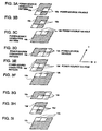
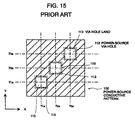
- a power-source conductive pattern 100a with power-source via holes 112 is formed on each of the 8aM layer, the 7aM layer, the 4am layer, and the 1aM.
- a power-source conductive pattern 100b is formed on each of the 6aM layer, the 3aM layer, and the 0aM layer.
- a power-source conductive pattern 100c is formed on each of the 5aM layer and the 2aM layer.
- the power-source via holes 112a to 112c are positioned in such a way that the projected positions of the power-source via holes 112a to 112c are not aligned with each other when the power-source conductive patterns 100a to 100c are piled up.
- both the power-source via hole 112b formed on the power-source conductive pattern 100b and the power-source via hole 112c formed on the power-source conductive pattern 100c are not electrically connected to the power-source via hole 112a in the power-source conductive pattern 100a because the power-source via hole 112a is arranged as shown in the above example.
- FIG. 19 is a plan view schematically and partially illustrating a conventional build-up board.
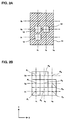
- FIG. 1A is a plan view illustrating a polyimide/ceramic multilayer wiring board according to a first embodiment of the present invention.
- FIG. 1B is a cross-sectional view schematically illustrating the polyimide/ceramic multilayer wiring board taken along the line A-A of FIG. 1A.
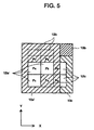
- the line segments X 1 , X 2 and X 3 and the line segments Y 1 , Y 2 and Y 3 shown in FIG. 2B correspond to those in FIG. 2A, respectively.
- P 1 to P 9 respectively represent cross points between the line segments.
- Areas surrounded by solid lines in FIG. 2B represent power-source via holes 12a, 12a', 12b, and 12c.
- three power-source via holes 12 in FIG. 2A are formed at the positions p 1 , P 4 and p 5 shown in FIG. 2B, respectively.
- a via hole is not formed at the position P 9 .
- the present invention should not be limited to only this embodiment. If necessary, a via hole may be formed at the position P 9 .
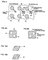
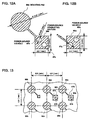
- Round mounting pads 86a and 86b are arranged at equal intervals, as shown in FIG. 8.
- the mounting pad 86a is electrically connected to two power-source via holes 87b for power supplying, which are formed on the square power-source conductive pattern 90b.
- the mounting pad 88b is electrically connected to the signal via hole 89 for signal transmission.
Landscapes
- Engineering & Computer Science (AREA)
- Microelectronics & Electronic Packaging (AREA)
- Production Of Multi-Layered Print Wiring Board (AREA)
Abstract
Description
Claims (6)
- A multilayer wiring board, comprising:a first wiring layer having a first wiring pattern;a second wiring layer having a second wiring pattern;the wiring direction of said first wiring pattern and the wiring direction of said second wiring pattern being substantially perpendicularly to each other, said first wiring layer and second wiring layer being laminated; anda plurality of conductive patterns formed on each of said first and second wiring layers in such a way that each of long sides is oriented substantially in the same direction as the wiring direction of a wiring pattern formed on each wiring layer, each of said conductive patterns in which a plurality of via holes are formed, each of said conductive patterns having a nearly rectangular form.
- The multilayer wiring board defined in claim 1,
wherein a position at which each via hole in each of said conductive patterns formed on said first wiring layer is projected is not aligned with a position at which each via hole in each of said conductive patterns formed on said second wiring layer. - The multilayer wiring board defined in Claim 1 or 2,
wherein a long side of each of said conductive patterns corresponds to the length along which at least three via holes can be formed and wherein a short side of each of said conductive patterns corresponds to the length along which at least two via holes can be formed. - The multilayer wiring board defined in Claim 2 or 3,
wherein at least two via holes are formed in each of said conductive patterns. - A multilayer wiring board comprising:a first wiring layer and a second wiring layer laminated to each other;a plurality of first conductive patterns arranged on said first wiring layer, each of said plurality of first conductive patterns having a plurality of power-source via holes; anda plurality of second conductive patterns arranged on said second wiring layer, each of said plurality of second conductive patterns having a plurality of power-source via holes at positions which are not aligned with positions where said via holes in said first pattern are projected.
- A multilayer wiring board, comprising:a first wiring layer and a second wiring layer laminated to each other;a plurality of first conductive patterns arranged on said first wiring layer, each of said plurality of first conductive patterns having a plurality of grounding via holes; anda plurality of second conductive patterns arranged on said second wiring layer, each of said plurality of second conductive patterns having a plurality of grounding via holes at positions which are not aligned with positions where said via holes in said first pattern are projected.
Applications Claiming Priority (2)
| Application Number | Priority Date | Filing Date | Title |
|---|---|---|---|
| JP20375699A JP3562568B2 (en) | 1999-07-16 | 1999-07-16 | Multilayer wiring board |
| JP20375699 | 1999-07-16 |
Publications (2)
| Publication Number | Publication Date |
|---|---|
| EP1069617A2 true EP1069617A2 (en) | 2001-01-17 |
| EP1069617A3 EP1069617A3 (en) | 2004-11-03 |
Family
ID=16479326
Family Applications (1)
| Application Number | Title | Priority Date | Filing Date |
|---|---|---|---|
| EP00114903A Withdrawn EP1069617A3 (en) | 1999-07-16 | 2000-07-14 | Multilayer wiring board |
Country Status (3)
| Country | Link |
|---|---|
| US (1) | US6407343B1 (en) |
| EP (1) | EP1069617A3 (en) |
| JP (1) | JP3562568B2 (en) |
Cited By (4)
| Publication number | Priority date | Publication date | Assignee | Title |
|---|---|---|---|---|
| WO2004017687A1 (en) * | 2002-05-23 | 2004-02-26 | International Business Machines Corporation | Improved structure of stacked vias in multiple layer electronic device carriers |
| US7240429B2 (en) | 2001-06-13 | 2007-07-10 | Denso Corporation | Manufacturing method for a printed circuit board |
| CN104377183A (en) * | 2013-08-16 | 2015-02-25 | 台湾积体电路制造股份有限公司 | Metal pad offset for multi-layer metal layout |
| EP4447622A4 (en) * | 2022-04-24 | 2025-04-16 | Huawei Technologies Co., Ltd. | ELECTRONIC DEVICE, AND PRINTED CIRCUIT BOARD AND METHOD FOR MANUFACTURING SAME |
Families Citing this family (18)
| Publication number | Priority date | Publication date | Assignee | Title |
|---|---|---|---|---|
| US20040212103A1 (en) * | 2000-06-19 | 2004-10-28 | Herman Kwong | Techniques for pin arrangements in circuit chips |
| US7069646B2 (en) * | 2000-06-19 | 2006-07-04 | Nortel Networks Limited | Techniques for reducing the number of layers in a multilayer signal routing device |
| US7725860B1 (en) | 2000-06-19 | 2010-05-25 | Herman Kwong | Contact mapping using channel routing |
| US7259336B2 (en) | 2000-06-19 | 2007-08-21 | Nortel Networks Limited | Technique for improving power and ground flooding |
| US7256354B2 (en) * | 2000-06-19 | 2007-08-14 | Wyrzykowska Aneta O | Technique for reducing the number of layers in a multilayer circuit board |
| US7107673B2 (en) * | 2000-06-19 | 2006-09-19 | Nortel Networks Limited | Technique for accommodating electronic components on a multiplayer signal routing device |
| US7281326B1 (en) | 2000-06-19 | 2007-10-16 | Nortel Network Limited | Technique for routing conductive traces between a plurality of electronic components of a multilayer signal routing device |
| US6602078B2 (en) * | 2001-03-16 | 2003-08-05 | Cenix, Inc. | Electrical interconnect having a multi-layer circuit board structure and including a conductive spacer for impedance matching |
| JP3864093B2 (en) * | 2002-01-10 | 2006-12-27 | シャープ株式会社 | Printed circuit board, radio wave receiving converter and antenna device |
| DE10205450A1 (en) * | 2002-02-08 | 2003-08-28 | Infineon Technologies Ag | Circuit carrier and manufacture of the same |
| US7405364B2 (en) * | 2002-12-30 | 2008-07-29 | Intel Corporation | Decoupled signal-power substrate architecture |
| JPWO2005024863A1 (en) * | 2003-09-01 | 2006-11-16 | 株式会社村田製作所 | Multilayer coil component and manufacturing method thereof |
| JP5201983B2 (en) * | 2007-12-28 | 2013-06-05 | 富士通株式会社 | Electronic components |
| TWI347810B (en) * | 2008-10-03 | 2011-08-21 | Po Ju Chou | A method for manufacturing a flexible pcb and the structure of the flexible pcb |
| KR20110113980A (en) * | 2010-04-12 | 2011-10-19 | 삼성전자주식회사 | Multilayer printed circuit board including film and manufacturing method thereof |
| KR101218985B1 (en) * | 2011-05-31 | 2013-01-04 | 삼성전기주식회사 | Chip-type coil component |
| US9275925B2 (en) | 2013-03-12 | 2016-03-01 | Taiwan Semiconductor Manufacturing Company, Ltd. | System and method for an improved interconnect structure |
| US10244629B1 (en) * | 2017-11-03 | 2019-03-26 | Innovium, Inc. | Printed circuit board including multi-diameter vias |
Family Cites Families (14)
| Publication number | Priority date | Publication date | Assignee | Title |
|---|---|---|---|---|
| FR2512315A1 (en) * | 1981-09-02 | 1983-03-04 | Rouge Francois | MULTI-LAYER ELECTRIC CIRCUIT BLANK AND METHOD FOR MANUFACTURING MULTILAYER CIRCUITS WITH APPLICATION |
| JPH023631Y2 (en) * | 1984-12-28 | 1990-01-29 | ||
| US5288949A (en) * | 1992-02-03 | 1994-02-22 | Ncr Corporation | Connection system for integrated circuits which reduces cross-talk |
| US5410107A (en) * | 1993-03-01 | 1995-04-25 | The Board Of Trustees Of The University Of Arkansas | Multichip module |
| JPH06291216A (en) * | 1993-04-05 | 1994-10-18 | Sony Corp | Substrate and ceramic package |
| US5378927A (en) * | 1993-05-24 | 1995-01-03 | International Business Machines Corporation | Thin-film wiring layout for a non-planar thin-film structure |
| JP3408590B2 (en) * | 1993-09-29 | 2003-05-19 | 富士通株式会社 | Wiring structure of multilayer printed circuit board |
| KR100194130B1 (en) * | 1994-03-30 | 1999-06-15 | 니시무로 타이죠 | Semiconductor package |
| US5574630A (en) * | 1995-05-11 | 1996-11-12 | International Business Machines Corporation | Laminated electronic package including a power/ground assembly |
| JP3287181B2 (en) * | 1995-08-15 | 2002-05-27 | ソニー株式会社 | Connection structure of multilayer wiring |
| JP3732927B2 (en) * | 1997-07-31 | 2006-01-11 | 京セラ株式会社 | Multilayer wiring board |
| US6175088B1 (en) * | 1998-10-05 | 2001-01-16 | Avaya Technology Corp. | Multi-layer printed-wiring boards with inner power and ground layers |
| US6201194B1 (en) * | 1998-12-02 | 2001-03-13 | International Business Machines Corporation | Multi-voltage plane, multi-signal plane circuit card with photoimageable dielectric |
| US6184477B1 (en) * | 1998-12-02 | 2001-02-06 | Kyocera Corporation | Multi-layer circuit substrate having orthogonal grid ground and power planes |
-
1999
- 1999-07-16 JP JP20375699A patent/JP3562568B2/en not_active Expired - Fee Related
-
2000
- 2000-07-13 US US09/615,942 patent/US6407343B1/en not_active Expired - Fee Related
- 2000-07-14 EP EP00114903A patent/EP1069617A3/en not_active Withdrawn
Cited By (6)
| Publication number | Priority date | Publication date | Assignee | Title |
|---|---|---|---|---|
| US7240429B2 (en) | 2001-06-13 | 2007-07-10 | Denso Corporation | Manufacturing method for a printed circuit board |
| WO2004017687A1 (en) * | 2002-05-23 | 2004-02-26 | International Business Machines Corporation | Improved structure of stacked vias in multiple layer electronic device carriers |
| CN104377183A (en) * | 2013-08-16 | 2015-02-25 | 台湾积体电路制造股份有限公司 | Metal pad offset for multi-layer metal layout |
| US9659859B2 (en) | 2013-08-16 | 2017-05-23 | Taiwan Semiconductor Manufacturing Company, Ltd. | Metal pad offset for multi-layer metal layout |
| CN104377183B (en) * | 2013-08-16 | 2017-06-13 | 台湾积体电路制造股份有限公司 | For the metal pad skew of multiple layer metal layout |
| EP4447622A4 (en) * | 2022-04-24 | 2025-04-16 | Huawei Technologies Co., Ltd. | ELECTRONIC DEVICE, AND PRINTED CIRCUIT BOARD AND METHOD FOR MANUFACTURING SAME |
Also Published As
| Publication number | Publication date |
|---|---|
| US6407343B1 (en) | 2002-06-18 |
| JP2001036247A (en) | 2001-02-09 |
| EP1069617A3 (en) | 2004-11-03 |
| JP3562568B2 (en) | 2004-09-08 |
Similar Documents
| Publication | Publication Date | Title |
|---|---|---|
| EP1069617A2 (en) | Multilayer wiring board | |
| US6344616B1 (en) | Cable capable of connecting between integrated circuit elements in a reduced space | |
| US6000130A (en) | Process for making planar redistribution structure | |
| US6281446B1 (en) | Multi-layered circuit board and method of manufacturing the same | |
| US5432677A (en) | Multi-chip integrated circuit module | |
| KR101218011B1 (en) | Flip chip interconnect pad layout semiconductor package and its production method | |
| EP0883330B1 (en) | Circuit board with primary and secondary through holes | |
| US5471090A (en) | Electronic structures having a joining geometry providing reduced capacitive loading | |
| US5847936A (en) | Optimized routing scheme for an integrated circuit/printed circuit board | |
| US6388200B2 (en) | Electronic interconnection medium having offset electrical mesh plane | |
| US5290971A (en) | Printed circuit board provided with a higher density of terminals for hybrid integrated circuit and method of fabricating the same | |
| JP2005515611A (en) | High performance low cost micro circuit package with interposer | |
| CN1203546C (en) | High density design for organic chip carrier | |
| US7243423B2 (en) | Chip package with degassing holes | |
| EP1075026A2 (en) | Multilayer circuit board layout | |
| US6121678A (en) | Wrap-around interconnect for fine pitch ball grid array | |
| EP0414204A2 (en) | Multilayer interconnection substrate and semiconductor integrated circuit device using the same | |
| EP0268111A2 (en) | Interposer chip technique for making engineering changes between interconnected semiconductor chips | |
| KR19990029636A (en) | Semiconductor chip | |
| US6946727B2 (en) | Vertical routing structure | |
| JP3408590B2 (en) | Wiring structure of multilayer printed circuit board | |
| US7105926B2 (en) | Routing scheme for differential pairs in flip chip substrates | |
| US5489500A (en) | Flexible strip structure for a parallel processor and method of fabricating the flexible strip | |
| US7143509B2 (en) | Circuit board and processing method thereof | |
| JPH02116195A (en) | Multilayer thick film hybrid integrated circuit |
Legal Events
| Date | Code | Title | Description |
|---|---|---|---|
| PUAI | Public reference made under article 153(3) epc to a published international application that has entered the european phase |
Free format text: ORIGINAL CODE: 0009012 |
|
| AK | Designated contracting states |
Kind code of ref document: A2 Designated state(s): AT BE CH CY DE DK ES FI FR GB GR IE IT LI LU MC NL PT SE |
|
| AX | Request for extension of the european patent |
Free format text: AL;LT;LV;MK;RO;SI |
|
| PUAL | Search report despatched |
Free format text: ORIGINAL CODE: 0009013 |
|
| AK | Designated contracting states |
Kind code of ref document: A3 Designated state(s): AT BE CH CY DE DK ES FI FR GB GR IE IT LI LU MC NL PT SE |
|
| AX | Request for extension of the european patent |
Extension state: AL LT LV MK RO SI |
|
| 17P | Request for examination filed |
Effective date: 20040924 |
|
| AKX | Designation fees paid |
Designated state(s): DE FR |
|
| STAA | Information on the status of an ep patent application or granted ep patent |
Free format text: STATUS: THE APPLICATION IS DEEMED TO BE WITHDRAWN |
|
| 18D | Application deemed to be withdrawn |
Effective date: 20060810 |