EP1069615A2 - Semiconductor device - Google Patents
Semiconductor device Download PDFInfo
- Publication number
- EP1069615A2 EP1069615A2 EP00305878A EP00305878A EP1069615A2 EP 1069615 A2 EP1069615 A2 EP 1069615A2 EP 00305878 A EP00305878 A EP 00305878A EP 00305878 A EP00305878 A EP 00305878A EP 1069615 A2 EP1069615 A2 EP 1069615A2
- Authority
- EP
- European Patent Office
- Prior art keywords
- interconnection wiring
- insulating layer
- external connection
- wiring lines
- terminals
- Prior art date
- Legal status (The legal status is an assumption and is not a legal conclusion. Google has not performed a legal analysis and makes no representation as to the accuracy of the status listed.)
- Withdrawn
Links
Images


Classifications
-
- H—ELECTRICITY
- H10—SEMICONDUCTOR DEVICES; ELECTRIC SOLID-STATE DEVICES NOT OTHERWISE PROVIDED FOR
- H10W—GENERIC PACKAGES, INTERCONNECTIONS, CONNECTORS OR OTHER CONSTRUCTIONAL DETAILS OF DEVICES COVERED BY CLASS H10
- H10W72/00—Interconnections or connectors in packages
- H10W72/20—Bump connectors, e.g. solder bumps or copper pillars; Dummy bumps; Thermal bumps
-
- H—ELECTRICITY
- H10—SEMICONDUCTOR DEVICES; ELECTRIC SOLID-STATE DEVICES NOT OTHERWISE PROVIDED FOR
- H10W—GENERIC PACKAGES, INTERCONNECTIONS, CONNECTORS OR OTHER CONSTRUCTIONAL DETAILS OF DEVICES COVERED BY CLASS H10
- H10W72/00—Interconnections or connectors in packages
- H10W72/90—Bond pads, in general
-
- H—ELECTRICITY
- H10—SEMICONDUCTOR DEVICES; ELECTRIC SOLID-STATE DEVICES NOT OTHERWISE PROVIDED FOR
- H10W—GENERIC PACKAGES, INTERCONNECTIONS, CONNECTORS OR OTHER CONSTRUCTIONAL DETAILS OF DEVICES COVERED BY CLASS H10
- H10W70/00—Package substrates; Interposers; Redistribution layers [RDL]
- H10W70/60—Insulating or insulated package substrates; Interposers; Redistribution layers
-
- H—ELECTRICITY
- H10—SEMICONDUCTOR DEVICES; ELECTRIC SOLID-STATE DEVICES NOT OTHERWISE PROVIDED FOR
- H10W—GENERIC PACKAGES, INTERCONNECTIONS, CONNECTORS OR OTHER CONSTRUCTIONAL DETAILS OF DEVICES COVERED BY CLASS H10
- H10W72/00—Interconnections or connectors in packages
- H10W72/20—Bump connectors, e.g. solder bumps or copper pillars; Dummy bumps; Thermal bumps
- H10W72/241—Dispositions, e.g. layouts
- H10W72/242—Dispositions, e.g. layouts relative to the surface, e.g. recessed, protruding
-
- H—ELECTRICITY
- H10—SEMICONDUCTOR DEVICES; ELECTRIC SOLID-STATE DEVICES NOT OTHERWISE PROVIDED FOR
- H10W—GENERIC PACKAGES, INTERCONNECTIONS, CONNECTORS OR OTHER CONSTRUCTIONAL DETAILS OF DEVICES COVERED BY CLASS H10
- H10W72/00—Interconnections or connectors in packages
- H10W72/20—Bump connectors, e.g. solder bumps or copper pillars; Dummy bumps; Thermal bumps
- H10W72/241—Dispositions, e.g. layouts
- H10W72/244—Dispositions, e.g. layouts relative to underlying supporting features, e.g. bond pads, RDLs or vias
-
- H—ELECTRICITY
- H10—SEMICONDUCTOR DEVICES; ELECTRIC SOLID-STATE DEVICES NOT OTHERWISE PROVIDED FOR
- H10W—GENERIC PACKAGES, INTERCONNECTIONS, CONNECTORS OR OTHER CONSTRUCTIONAL DETAILS OF DEVICES COVERED BY CLASS H10
- H10W72/00—Interconnections or connectors in packages
- H10W72/20—Bump connectors, e.g. solder bumps or copper pillars; Dummy bumps; Thermal bumps
- H10W72/251—Materials
-
- H—ELECTRICITY
- H10—SEMICONDUCTOR DEVICES; ELECTRIC SOLID-STATE DEVICES NOT OTHERWISE PROVIDED FOR
- H10W—GENERIC PACKAGES, INTERCONNECTIONS, CONNECTORS OR OTHER CONSTRUCTIONAL DETAILS OF DEVICES COVERED BY CLASS H10
- H10W72/00—Interconnections or connectors in packages
- H10W72/20—Bump connectors, e.g. solder bumps or copper pillars; Dummy bumps; Thermal bumps
- H10W72/29—Bond pads specially adapted therefor
-
- H—ELECTRICITY
- H10—SEMICONDUCTOR DEVICES; ELECTRIC SOLID-STATE DEVICES NOT OTHERWISE PROVIDED FOR
- H10W—GENERIC PACKAGES, INTERCONNECTIONS, CONNECTORS OR OTHER CONSTRUCTIONAL DETAILS OF DEVICES COVERED BY CLASS H10
- H10W72/00—Interconnections or connectors in packages
- H10W72/50—Bond wires
- H10W72/531—Shapes of wire connectors
- H10W72/536—Shapes of wire connectors the connected ends being ball-shaped
-
- H—ELECTRICITY
- H10—SEMICONDUCTOR DEVICES; ELECTRIC SOLID-STATE DEVICES NOT OTHERWISE PROVIDED FOR
- H10W—GENERIC PACKAGES, INTERCONNECTIONS, CONNECTORS OR OTHER CONSTRUCTIONAL DETAILS OF DEVICES COVERED BY CLASS H10
- H10W72/00—Interconnections or connectors in packages
- H10W72/50—Bond wires
- H10W72/59—Bond pads specially adapted therefor
-
- H—ELECTRICITY
- H10—SEMICONDUCTOR DEVICES; ELECTRIC SOLID-STATE DEVICES NOT OTHERWISE PROVIDED FOR
- H10W—GENERIC PACKAGES, INTERCONNECTIONS, CONNECTORS OR OTHER CONSTRUCTIONAL DETAILS OF DEVICES COVERED BY CLASS H10
- H10W72/00—Interconnections or connectors in packages
- H10W72/90—Bond pads, in general
- H10W72/941—Dispositions of bond pads
- H10W72/942—Dispositions of bond pads relative to underlying supporting features, e.g. bond pads, RDLs or vias
Definitions
- the present invention relates to a chip size package, i.e., a semiconductor device having substantially the same size as that of a semiconductor chip included therein.
- a chip size package is a semiconductor device having substantially the same size as that of a semiconductor chip included therein and having an electrode terminal carrying surface including electrode terminals, electrically connected to external connection terminals, in the form of solder balls, etc.
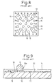
- Figure 7 shows a cross-sectional view of a CSP including a semiconductor chip 10 and external connection terminals 12, which are arranged entirely over an electrode carrying surface 11 of the semiconductor chip 10 that has a very small area.
- a protective film 14 protects the electrode carrying surface 11.
- Figure 8 is a plan view showing an arrayed arrangement of external connection terminals 12 over the electrode carrying surface 11 of the semiconductor chip 10.
- the arrangement of the electrode terminals 16 on the electrode terminal carrying surface 11 varies with the types of CSP 10.
- the shown type of semiconductor chip includes the electrode terminals 16 arranged along the periphery of the electrode terminal carrying surface 11 and interconnection wiring lines 18 outwardly extending from the arrayed external connection terminals 12 to the electrode terminals 16 to provide electrical connection between the electrode terminals 16 and the external connection terminals 12.
- Figure 9 is an enlarged partial cross-sectional view showing that the interconnection wiring lines 18 have a part forming a land 18a with a sufficient size for bonding to the external connection terminals 12, i.e., the interconnection wiring lines 18 have one end bonded to the electrode terminals 16 and the other end forming the land 18a positioned for bonding to the external connection terminals 12.
- An insulating layer 20 covers the surface of the semiconductor chip 10 and has openings at positions corresponding to the electrode terminals 16. After the insulating layer 20 having the openings is formed on the electrode terminal carrying surface 11 of the semiconductor chip 10, a conductor layer is formed on the insulating layer 20, by sputtering, etc., and is then patterned by etching to form the interconnection wiring lines 18 each having one end forming a land 18a.
- a chip size package has a problem that, as the number or density of the external connection terminals 12 is increased, the space between neighboring external connection terminals 12 becomes too small to allow the interconnection wiring lines 18 to run therethrough. There may be a case in which a plurality of interconnection wiring lines 18 must run through the space between neighboring external connection terminals 12.
- CSPs will have a further increased number of in/out terminals or external connection terminals to provide multipin CSPs, and in an extreme case, it may not be possible to run interconnection wiring lines 18 through the space between neighboring external connection terminals 12.
- the object of the present invention is to go at least some way towards providing a CSP or a semiconductor device having substantially the same size as that of a semiconductor chip included therein, particularly a multipin CSP structure which enables interconnection wiring lines connecting electrode terminals with external connection terminals to be easily provided for semiconductor chips having increased number or density of external connection terminals as in/out terminals.
- a semiconductor device including a semiconductor chip having electrode terminals electrically connected to external connection terminals, the semiconductor chip having an electrode terminal carrying surface including the electrode terminals and interconnection wiring lines, each of the interconnection wiring lines having one end bonded to one of the electrode terminals and the other end forming a pad;
- the lands are smaller in diameter than the pad.
- the via is preferably formed of a conductor layer coating a side wall and a bottom of a through hole penetrating the insulating layer, the bottom of the through hole being defined by a surface of the interconnection wiring lines.
- the lands occupy areas of the insulating layer that overlap areas of the electrode terminal carrying surface that are occupied by the interconnection wiring lines.
- FIG. 1 is a partial cross-sectional view showing a semiconductor device structure according to a preferred embodiment of the present invention.
- the shown device structure includes a semiconductor chip 10 having an electrode terminal carrying surface 11 having an electrode terminal (not shown) formed thereon and electrically connected to an external connection terminal or solder ball 12 through an interconnection wiring line 30 having one end (a first end, not shown) bonded to the electrode terminal and the other end (a second end) forming a pad 30a bonded to a via 36 defined by a part of a conductor land 32 bonded to the external connection terminal 12 formed thereon, in which the interconnection wiring line 30 and the land 32 are disposed on the electrode terminal carrying surface 11 and on an insulating layer 34, respectively, to prevent mutual interference therebetween while providing electrical connection therebetween through the via 30a.
- the interconnection wiring line 30 is formed on an insulating layer 20 coating the electrode terminal carrying surface 11 of the semiconductor chip 10 and has one end (the first end) bonded to an electrode terminal of the chip 10.
- the conventional semiconductor device as shown in Fig. 9, has an interconnection wiring line 18 having one end (a first end) bonded to an electrode terminal 16 of a semiconductor chip 10 and the other end (a second end) forming a conductor land 18a bonded to an external connection terminal or solder ball 12.
- the interconnection wiring line 30 has the second end forming a pad 30a connected to the land 32 through the via 36 penetrating through the insulating layer 34 intervening between the interconnection wiring line 30 and the land 32.
- the pad 30a forms a part of the interconnection wiring line 30, electrically connects the interconnection wiring line 30 to the land 32 through the via 36 and has a diameter equivalent to the width of the interconnection wiring line 30 and smaller than the diameter of the land 32.
- the via 36 is formed by first forming a via hole penetrating through the insulating layer 34 so that the pad 30a is exposed to define the bottom of the via hole and then coating the inner surface of the via hole with a conductor layer.
- the land 32 has a diameter far greater than the width of the interconnection wiring line 30.
- the positional relationship between the land 32, or the external connection terminal or solder ball 12, and the interconnection wiring line 30 is shown by Fig. 1 in a cross-sectional view or by Fig. 2 in a plan view.
- the interconnection wiring line 30 and the land 32 form separate layers with the insulating layer 34 intervening therebetween, so that the interconnection wiring line 30 and the land 32 can occupy areas overlapping on a plan view, i.e., the former runs under the latter without mutual interference except for the intended connection between the pad 30a and the via 36.
- the conventional semiconductor device has a structure in which interconnection wiring lines and external connection terminals are disposed in the same layer, i.e., on an electrode terminal carrying surface of a semiconductor chip, and the number or density of the external connection terminals is limited because spaces between the external connection terminals must be sufficient for the interconnection wiring lines(s) running therethrough in order to prevent interference between the interconnection wiring lines and the external connection terminals.
- external connection terminals are disposed on lands formed on a surface of an insulating layer separate from an electrode terminal carrying surface on which interconnection wiring lines are formed, so that the interconnection wiring lines can run through the areas of the electrode terminal carrying surface that were conventionally occupied by the external connection terminals and so that the areas for the interconnection wiring lines and the external connection terminals are substantially increased to provide a semiconductor device with an increased number or density of the external connection terminals.
- the interconnection wiring line 30 is designed to be connected at one end to an electrode terminal of the semiconductor chip 10 and to be connected at the other end forming the pad 30a to the land 32.
- the pad 30a is formed at a position for bonding to the land 32 through the via 36 formed by a part of the land 32.
- the land 32 shown in Fig. 2 has the via 36 at its center, the position of the via 36 is not necessarily so limited but may be formed by any part of the land 32.
- the pad 30a is designed to be positioned within an area in a top plan view that is occupied by the land 32 and the land 32 is designed to have a part forming the via 36 that corresponds to the position of the pad 30a. This provides an improved freedom of designing the arrangement of the interconnection wiring lines, including the pads, with respect to the positions of the lands or the external connection terminals.
- Figure 3 shows a semiconductor device according to another preferred embodiment of the present invention, in which the external connection terminal 12 is in the form of a lead pin in replacement for a solder ball.
- a land 32 is formed on an insulating layer 34 which covers an interconnection wiring line 30, a via 36 electrically connects the interconnection wiring line 30 with the land 32 and an external connection terminal or lead pin 12 standing on and bonded to, the land 32.
- Solder 40 bonds the lead pin 12 to the land 32.
- the interconnection wiring line 30 is arranged to cause no interference with the external connection terminal or lead pin 12.
- a protective film 38 protects the surface of the insulating layer 34 on which surface the land 32 is formed.
- the semiconductor device shown in Figs. 1 and 2 can be produced through the process steps shown in Figs. 4 and 5.
- Figure 4 shows the process steps for forming interconnection wiring lines on an electrode terminal carrying surface of a semiconductor chip.
- an insulating layer 20 is formed on an electrode terminal carrying surface 11 of a semiconductor chip 10, by either applying a polyimide or other insulating resin or bonding an insulating resin film to the electrode terminal carrying surface 11.
- the insulating layer 20 is chemically etched or laser-irradiated to form an opening through which an electrode terminal 16 of the semiconductor chip 10 is exposed.
- a conductor layer 42 is formed to cover the insulating layer 20 and the opening including the side wall thereof and the exposed surface of the electrode terminal 16, by sputtering, plating, or other suitable coating method.
- the conductor layer 42 having a desired thickness is preferably formed by forming a thin conductor layer by sputtering or by electroless copper plating, followed by electrolytic copper plating using the thin conductor layer as a current supply layer.
- the conductor layer 42 is patterned by chemical etching to form interconnection wiring lines 30. Specifically, a photosensitive resist is applied to the surface of the conductor layer 42, the thus-formed resist layer is exposed to light and developed to form a resist pattern having a reversed pattern of the interconnection wiring 30, the conductor layer 42 is etched using the resist pattern as an etching mask, and the resist pattern is removed by dissolution to leave the patterned interconnection wiring 30 on the insulating layer 20.
- the each interconnection wiring line 30 has one end connected to the electrode terminal 16 of the semiconductor chip 10 and the other end forming the pad 30a.
- an insulating layer 34 is formed by applying a polyimide or other insulating resin or by bonding an insulating resin film to the surface on which the interconnection wiring line 30 is formed.
- Figure 5 shows the process steps for forming a land 32 on the insulating layer 34, the land 32 being electrically connected to the interconnection wiring line 30.
- the insulating layer 34 is either etched or laser-irradiated to form a via hole 34a penetrating through the insulating layer 34 to expose the upper surface of the pad 30a of the interconnection wiring line 30.
- the via hole 34 has a side wall defined by an exposed surface of the insulating layer 34 and a bottom defined by the exposed upper surface of the pad 30a.
- the via hole 34 is positioned on the pad 30a of the interconnection wiring line 30 and defines the site for forming a via providing electrical connection between the pad 30a and a land on the insulating layer 34.
- a conductor layer 44 is formed by sputtering or plating to cover the insulating layer 34 and the via hole 34a.
- the conductor layer 44 adheres to the side wall and bottom of the via hole 34a.
- the conductor layer 34 may be thickened, if necessary, by further electrolytic copper plating, etc.
- the conductor layer 44 is patterned by etching to form a land 32 on the insulating layer 34, i.e., by forming on the conductor layer 44 a resist pattern having a reversed pattern of the land 32 and etching the conductor layer 44 using the resist pattern as an etching mask, as mentioned above referring to Fig. 4(d).
- the thus-formed land 32 lies on the insulating layer 34 and has a part forming a via 36 filling the via hole 34a and electrically connecting the land 32 with the pad 30a of the underlying interconnection wiring line 30.
- the land 32 may be further plated with a protective film of gold, etc.
- a solder resist or other protective film 38 is formed on the surface on which the land 32 is formed, to cover the surface except for the area occupied by the land 32.
- a solder ball 12 as an external connection terminal is formed on, and bonded to, the land 32, typically by placing a solder ball on the land 32 and reflowing the solder ball, to complete a semiconductor device according to the present invention, in which the interconnection wiring line 30 and the land 32 are separated from each other by the intervening insulating layer 34 except for the via 36 connecting the interconnection wiring line 30 with the land 32 to consequently provide electrical connection between the electrode terminal 16 of the semiconductor chip 10 and the external connection terminal 12 through the interconnection wiring line 30.
- the interconnection wiring line 30 and the land 32 may be formed by other methods as follows.
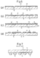
- the interconnection wiring line 30 may be formed by a so-called semi-additive process as shown in Fig. 6.
- sputtering or electroless copper plating is carried out to form a current supply layer or thin conductor layer 46 on the insulating layer 20 including the opening having a side wall and a bottom defined by the exposed surface of the electrode terminal 16.
- a photosensitive resist is then applied to the surface of the thin conductor layer 46, followed by exposure to light and development to form a resist pattern 48 having a reversed pattern of the interconnection wiring 30.
- electrolytic copper plating is carried out to form a conductor layer 50 on the thin conductor layer 46 in the portions exposed through the resist pattern 48.
- the resist pattern 48 is removed by solution thereof to leave the conductor layer 50 in a patterned form and the underlying thin conductor layer 46 in a continuous form. Chemical etching is then carried out to only remove the thin conductor layer 46 in the portions exposed through the patterned conductor layer 50, thereby completing an interconnection wiring line 30 lying on the insulating layer 20 and being composed of an upper substantial portion of the conductor layer 50 and a lower portion of the thin conductor layer 46.
- the thin conductor layer 46 is only necessary to provide a current supply layer for the subsequent electrolytic plating of the conductor layer 50 and can be extremely thin to be easily removed by etching while causing no substantial etching of the conductor layer 50 in the absence of a resist or other protection.
- the land 32 on the insulating layer 34 shown in Fig. 5(c) may be formed by the above-described process.
- an insulating layer 34 is formed to cover the interconnection wiring 30, a thin conductor layer for electrolytic plating is formed on the insulating layer 34, a resist pattern having a reversed pattern of the land 32 is formed on the thin conductor layer, electrolytic copper plating is carried out to form the land 32 on the thin conductor layer in the portion exposed through the resist pattern, the resist pattern is then removed by solution thereof, and the thus-exposed portion of the thin conductor layer is removed to leave the land 32 on the insulating layer 34.
- a plurality of semiconductor devices may be otherwise collectively produced on the same wafer by the same process as described referring to Figs. 4 to 6 and the wafer is then cut to plural semiconductor devices each including a single piece of the semiconductor chip 10.
- the present invention provides a semiconductor device having interconnection wiring lines 30 on a layer separate from a layer of the external connection terminals 12, so that the interconnection wiring lines 30 can be arranged more freely with respect to the arrangement of the external connection terminals 12 and the number or density of the external connection terminals 12 can be further increased to facilitate production of multipin CSPs without using multilayer interconnection wiring required in the conventional CSP structure.
Landscapes
- Internal Circuitry In Semiconductor Integrated Circuit Devices (AREA)
Abstract
Description
Claims (4)
- A semiconductor device including a semiconductor chip (10) having electrode terminals (16) electrically connected to external connection terminals (12), the semiconductor device chip (10) having an electrode terminal carrying surface (11) including the electrode terminals (16) and interconnection wiring lines (30), each of the interconnection wiring lines (30) having one end bonded to one of the electrode terminals (16) and the other end forming a pad (30a);an insulating layer (34) formed over the electrode terminal carrying surface (11) to cover the electrode terminals (16), the interconnection wiring lines (30) and the remaining area of the electrode terminal carrying surface (11);conductor lands (32) formed on the insulating layer (34), each of the conductor lands (32) having a part forming a via (36) extending through the insulating layer (34) to the pad (30a) of one of the interconnection wiring lines (30); andthe external connection terminals (12) formed on the lands (32).
- A semiconductor device according to claim 1, wherein the lands (32) are smaller in diameter than the pads (30a)
- A semiconductor device according to claim 1 or claim 2, wherein the via (36) is formed of a conductor layer (44) coating a side wall and a bottom of a through hole (34a) penetrating the insulating layer (34), the bottom of the through hole (34a) being defined by a surface of an interconnection wiring line (30).
- A semiconductor device according to any one of the preceding claims, wherein the lands (32) occupy areas of the insulating layer (34) that overlap areas of the electrode terminal carrying surface (11) that are occupied by the interconnection wiring lines (30).
Applications Claiming Priority (2)
| Application Number | Priority Date | Filing Date | Title |
|---|---|---|---|
| JP19866899 | 1999-07-13 | ||
| JP19866899A JP3606769B2 (en) | 1999-07-13 | 1999-07-13 | Semiconductor device |
Publications (2)
| Publication Number | Publication Date |
|---|---|
| EP1069615A2 true EP1069615A2 (en) | 2001-01-17 |
| EP1069615A3 EP1069615A3 (en) | 2002-04-03 |
Family
ID=16395068
Family Applications (1)
| Application Number | Title | Priority Date | Filing Date |
|---|---|---|---|
| EP00305878A Withdrawn EP1069615A3 (en) | 1999-07-13 | 2000-07-12 | Semiconductor device |
Country Status (3)
| Country | Link |
|---|---|
| US (1) | US6465886B1 (en) |
| EP (1) | EP1069615A3 (en) |
| JP (1) | JP3606769B2 (en) |
Cited By (3)
| Publication number | Priority date | Publication date | Assignee | Title |
|---|---|---|---|---|
| WO2003079434A3 (en) * | 2002-03-13 | 2004-03-11 | Motorola Inc | Semiconductor device having a wire bond pad and method therefor |
| WO2011047479A1 (en) | 2009-10-23 | 2011-04-28 | Ati Technologies Ulc | A routing layer for mitigating stress in a semiconductor die |
| WO2012142701A1 (en) | 2011-04-22 | 2012-10-26 | Ati Technologies Ulc | A routing layer for mitigating stress in a semiconductor die |
Families Citing this family (16)
| Publication number | Priority date | Publication date | Assignee | Title |
|---|---|---|---|---|
| TW448524B (en) * | 1997-01-17 | 2001-08-01 | Seiko Epson Corp | Electronic component, semiconductor device, manufacturing method therefor, circuit board and electronic equipment |
| US7005727B2 (en) * | 2001-12-28 | 2006-02-28 | Intel Corporation | Low cost programmable CPU package/substrate |
| JP3678239B2 (en) * | 2003-06-30 | 2005-08-03 | セイコーエプソン株式会社 | Semiconductor device and manufacturing method thereof, circuit board, and electronic apparatus |
| JP2008140886A (en) * | 2006-11-30 | 2008-06-19 | Shinko Electric Ind Co Ltd | Wiring board and manufacturing method thereof |
| TWI337059B (en) * | 2007-06-22 | 2011-02-01 | Princo Corp | Multi-layer substrate and manufacture method thereof |
| US8349721B2 (en) * | 2008-03-19 | 2013-01-08 | Stats Chippac, Ltd. | Semiconductor device and method of forming insulating layer on conductive traces for electrical isolation in fine pitch bonding |
| US7683493B2 (en) * | 2008-04-29 | 2010-03-23 | International Business Machines Corporation | Intermetallic diffusion block device and method of manufacture |
| JP5544872B2 (en) | 2009-12-25 | 2014-07-09 | 富士通セミコンダクター株式会社 | Semiconductor device and manufacturing method thereof |
| US9224688B2 (en) * | 2013-01-04 | 2015-12-29 | Taiwan Semiconductor Manufacturing Company, Ltd. | Metal routing architecture for integrated circuits |
| US9508637B2 (en) | 2014-01-06 | 2016-11-29 | Taiwan Semiconductor Manufacturing Company, Ltd. | Protrusion bump pads for bond-on-trace processing |
| US9418928B2 (en) | 2014-01-06 | 2016-08-16 | Taiwan Semiconductor Manufacturing Company, Ltd. | Protrusion bump pads for bond-on-trace processing |
| US9275967B2 (en) | 2014-01-06 | 2016-03-01 | Taiwan Semiconductor Manufacturing Company, Ltd. | Protrusion bump pads for bond-on-trace processing |
| US9305890B2 (en) | 2014-01-15 | 2016-04-05 | Taiwan Semiconductor Manufacturing Company, Ltd. | Package having substrate with embedded metal trace overlapped by landing pad |
| KR102793907B1 (en) * | 2020-08-24 | 2025-04-08 | 삼성전자주식회사 | semiconductor package |
| US11862588B2 (en) * | 2021-01-14 | 2024-01-02 | Taiwan Semiconductor Manufacturing Co., Ltd. | Semiconductor device and method |
| JP7715590B2 (en) | 2021-09-27 | 2025-07-30 | 新光電気工業株式会社 | Wiring board and method of manufacturing the same |
Family Cites Families (5)
| Publication number | Priority date | Publication date | Assignee | Title |
|---|---|---|---|---|
| JPS59181041A (en) * | 1983-03-31 | 1984-10-15 | Toshiba Corp | Semiconductor integrated circuit device |
| DE69014871T2 (en) * | 1990-07-31 | 1995-05-24 | Ibm | Process for the formation of metallic contact surfaces and connections on semiconductor chips. |
| EP0734059B1 (en) * | 1995-03-24 | 2005-11-09 | Shinko Electric Industries Co., Ltd. | Chip sized semiconductor device and a process for making it |
| US5723822A (en) * | 1995-03-24 | 1998-03-03 | Integrated Device Technology, Inc. | Structure for fabricating a bonding pad having improved adhesion to an underlying structure |
| JPH10284634A (en) * | 1997-04-03 | 1998-10-23 | Matsushita Electron Corp | Semiconductor device and manufacture therefor |
-
1999
- 1999-07-13 JP JP19866899A patent/JP3606769B2/en not_active Expired - Fee Related
-
2000
- 2000-07-12 EP EP00305878A patent/EP1069615A3/en not_active Withdrawn
- 2000-07-13 US US09/615,558 patent/US6465886B1/en not_active Expired - Lifetime
Cited By (8)
| Publication number | Priority date | Publication date | Assignee | Title |
|---|---|---|---|---|
| WO2003079434A3 (en) * | 2002-03-13 | 2004-03-11 | Motorola Inc | Semiconductor device having a wire bond pad and method therefor |
| US6846717B2 (en) | 2002-03-13 | 2005-01-25 | Freescale Semiconductor, Inc. | Semiconductor device having a wire bond pad and method therefor |
| WO2011047479A1 (en) | 2009-10-23 | 2011-04-28 | Ati Technologies Ulc | A routing layer for mitigating stress in a semiconductor die |
| EP2471096A4 (en) * | 2009-10-23 | 2015-04-29 | Ati Technologies Ulc | ROUTING LAYER FOR MITIGATION OF CONSTRAINTS IN A SEMICONDUCTOR CHIP |
| US9035471B2 (en) | 2009-10-23 | 2015-05-19 | Ati Technologies Ulc | Routing layer for mitigating stress in a semiconductor die |
| US9059159B2 (en) | 2009-10-23 | 2015-06-16 | Ati Technologies Ulc | Routing layer for mitigating stress in a semiconductor die |
| WO2012142701A1 (en) | 2011-04-22 | 2012-10-26 | Ati Technologies Ulc | A routing layer for mitigating stress in a semiconductor die |
| EP2700091A4 (en) * | 2011-04-22 | 2015-04-29 | Ati Technologies Ulc | INTERCONNECT LAYER FOR MITIGATING CONSTRAINTS IN A SEMICONDUCTOR CHIP |
Also Published As
| Publication number | Publication date |
|---|---|
| US6465886B1 (en) | 2002-10-15 |
| JP2001024023A (en) | 2001-01-26 |
| JP3606769B2 (en) | 2005-01-05 |
| EP1069615A3 (en) | 2002-04-03 |
Similar Documents
| Publication | Publication Date | Title |
|---|---|---|
| US6465886B1 (en) | Semiconductor device having circuit pattern and lands thereon | |
| US7208349B2 (en) | Package substrate manufactured using electrolytic leadless plating process, and method for manufacturing the same | |
| US6041495A (en) | Method of manufacturing a circuit board having metal bumps and a semiconductor device package comprising the same | |
| US6872590B2 (en) | Package substrate for electrolytic leadless plating and manufacturing method thereof | |
| KR100499003B1 (en) | A package substrate for electrolytic leadless plating, and its manufacturing method | |
| US7670962B2 (en) | Substrate having stiffener fabrication method | |
| KR101168263B1 (en) | Semiconductor package and fabrication method thereof | |
| KR100389314B1 (en) | Making method of PCB | |
| US20050054187A1 (en) | Method for forming ball pads of BGA substrate | |
| KR20190136240A (en) | Package board and method of manufacturing the same | |
| US7202421B2 (en) | Electronic elements, method for manufacturing electronic elements, circuit substrates, method for manufacturing circuit substrates, electronic devices and method for manufacturing electronic devices | |
| CN1059982C (en) | Method for manufacturing integrated circuit package circuit board | |
| CN101305453B (en) | Fine pitch interconnect and method of manufacture | |
| US6867122B2 (en) | Redistribution process | |
| US6240632B1 (en) | Method of manufacturing lead frame and integrated circuit package | |
| EP1003209A1 (en) | Process for manufacturing semiconductor device | |
| JP2001024097A (en) | Chip package substrate structure and manufacturing method thereof | |
| US11749596B2 (en) | Wiring substrate | |
| JP2000114412A (en) | Circuit board manufacturing method | |
| CN101916751B (en) | Encapsulation structure and manufacturing method thereof | |
| US6646357B2 (en) | Semiconductor device and method of production of same | |
| KR100599636B1 (en) | Manufacturing Method of Printed Circuit Board for BOS Semiconductor Packages | |
| JP3656590B2 (en) | Manufacturing method of tape carrier for semiconductor device | |
| CN108630555A (en) | Semiconductor package structure and manufacturing method thereof | |
| KR100325459B1 (en) | Chip size package manufacturing method |
Legal Events
| Date | Code | Title | Description |
|---|---|---|---|
| PUAI | Public reference made under article 153(3) epc to a published international application that has entered the european phase |
Free format text: ORIGINAL CODE: 0009012 |
|
| AK | Designated contracting states |
Kind code of ref document: A2 Designated state(s): DE FR GB Kind code of ref document: A2 Designated state(s): AT BE CH CY DE DK ES FI FR GB GR IE IT LI LU MC NL PT SE |
|
| AX | Request for extension of the european patent |
Free format text: AL;LT;LV;MK;RO;SI |
|
| PUAL | Search report despatched |
Free format text: ORIGINAL CODE: 0009013 |
|
| AK | Designated contracting states |
Kind code of ref document: A3 Designated state(s): AT BE CH CY DE DK ES FI FR GB GR IE IT LI LU MC NL PT SE |
|
| AX | Request for extension of the european patent |
Free format text: AL;LT;LV;MK;RO;SI |
|
| 17P | Request for examination filed |
Effective date: 20020912 |
|
| AKX | Designation fees paid |
Free format text: DE FR GB |
|
| 17Q | First examination report despatched |
Effective date: 20050315 |
|
| STAA | Information on the status of an ep patent application or granted ep patent |
Free format text: STATUS: THE APPLICATION IS DEEMED TO BE WITHDRAWN |
|
| 18D | Application deemed to be withdrawn |
Effective date: 20060613 |