EP1069554A1 - Détecteur de puissance à gigue faible pour communications par accès multiple et à division dans le temps - Google Patents
Détecteur de puissance à gigue faible pour communications par accès multiple et à division dans le temps Download PDFInfo
- Publication number
- EP1069554A1 EP1069554A1 EP99600019A EP99600019A EP1069554A1 EP 1069554 A1 EP1069554 A1 EP 1069554A1 EP 99600019 A EP99600019 A EP 99600019A EP 99600019 A EP99600019 A EP 99600019A EP 1069554 A1 EP1069554 A1 EP 1069554A1
- Authority
- EP
- European Patent Office
- Prior art keywords
- signal
- value
- date
- binary
- threshold
- Prior art date
- Legal status (The legal status is an assumption and is not a legal conclusion. Google has not performed a legal analysis and makes no representation as to the accuracy of the status listed.)
- Withdrawn
Links
- 238000004891 communication Methods 0.000 title claims abstract description 15
- 238000001914 filtration Methods 0.000 claims abstract description 13
- 238000000034 method Methods 0.000 claims abstract description 10
- 238000012545 processing Methods 0.000 claims description 22
- 238000005259 measurement Methods 0.000 claims description 17
- 230000007704 transition Effects 0.000 claims description 14
- 238000001514 detection method Methods 0.000 claims description 8
- 230000003111 delayed effect Effects 0.000 claims description 6
- 238000012935 Averaging Methods 0.000 claims description 4
- 238000005070 sampling Methods 0.000 claims description 3
- 230000003213 activating effect Effects 0.000 claims 2
- 230000005540 biological transmission Effects 0.000 abstract description 14
- 230000003287 optical effect Effects 0.000 abstract 1
- 238000010586 diagram Methods 0.000 description 7
- 238000009499 grossing Methods 0.000 description 6
- 238000013459 approach Methods 0.000 description 3
- 230000007246 mechanism Effects 0.000 description 3
- 238000009432 framing Methods 0.000 description 2
- 238000011084 recovery Methods 0.000 description 2
- 230000000630 rising effect Effects 0.000 description 2
- 238000001228 spectrum Methods 0.000 description 2
- 238000006243 chemical reaction Methods 0.000 description 1
- 230000000694 effects Effects 0.000 description 1
- 238000005516 engineering process Methods 0.000 description 1
- 238000000605 extraction Methods 0.000 description 1
- 238000010295 mobile communication Methods 0.000 description 1
- 230000011664 signaling Effects 0.000 description 1
Images


Classifications
-
- H—ELECTRICITY
- H04—ELECTRIC COMMUNICATION TECHNIQUE
- H04B—TRANSMISSION
- H04B17/00—Monitoring; Testing
- H04B17/10—Monitoring; Testing of transmitters
- H04B17/15—Performance testing
- H04B17/18—Monitoring during normal operation
-
- H—ELECTRICITY
- H04—ELECTRIC COMMUNICATION TECHNIQUE
- H04B—TRANSMISSION
- H04B17/00—Monitoring; Testing
- H04B17/10—Monitoring; Testing of transmitters
- H04B17/101—Monitoring; Testing of transmitters for measurement of specific parameters of the transmitter or components thereof
-
- H—ELECTRICITY
- H04—ELECTRIC COMMUNICATION TECHNIQUE
- H04B—TRANSMISSION
- H04B17/00—Monitoring; Testing
- H04B17/10—Monitoring; Testing of transmitters
- H04B17/101—Monitoring; Testing of transmitters for measurement of specific parameters of the transmitter or components thereof
- H04B17/102—Power radiated at antenna
-
- H—ELECTRICITY
- H04—ELECTRIC COMMUNICATION TECHNIQUE
- H04B—TRANSMISSION
- H04B17/00—Monitoring; Testing
- H04B17/10—Monitoring; Testing of transmitters
- H04B17/101—Monitoring; Testing of transmitters for measurement of specific parameters of the transmitter or components thereof
- H04B17/104—Monitoring; Testing of transmitters for measurement of specific parameters of the transmitter or components thereof of other parameters, e.g. DC offset, delay or propagation times
Definitions
- This invention relates to the detection of power in burst data transmission systems such as the time division multiple access (TDMA) communication systems, where low jitter is required for the power detect (PD) signal and the multiple access protocol employed by the transmission system can be an asynchronous one such as the ALOHA protocol.
- TDMA time division multiple access
- PD power detect
- a receive signal sense indicator represents a quality indicator of the transmission channel. Thresholding of this indicator produces the PD signal, that provides an alarm signal used at the same time to possibly suspend the operation of parameter recovery mechanisms such as clock and carrier recovery.
- PD time accuracy in such systems is not a crucial issue.
- a large number of wireless communication systems transmitting data in a burst by burst manner have been deployed that include fixed and mobile communication systems within a large spectrum of different modulation formats, topologies, capacities and access protocols.
- PD time accuracy and more particularly the rising edge of an active-high power detect signal directly affects the length of the preamble employed by such systems.
- the power detect task must be carried out in an economic way in terms of circuit complexity, so that the low power requirement, ordinary in wireless TDMA systems, will be satisfied.
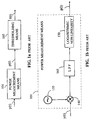
- FIG.1a shows a typical prior art power detector structure.
- a modulated carrier signal y(t) feeds a power measurement stage 101 producing an analogue signal p(t) which carries the power information of the received signal in a linear or logarithmic scale.
- the power detect signal r(t) is produced by comparing signal p(t) to a specified threshold.
- FIG.1b there is shown a specific schematic block diagram for the said processing stage 101 comprising successive steps of frequency down-conversion of the received signal y(t) by mixing with a reference waveform produced by a local oscillator 135, smoothing by a lowpass filter 185 and optionally undergoing a logarithmic rule 170.
- a power measurement means 102 produces the signal p(t) carrying the power information.
- the signal p(t) is sampled, and the sampled power detect signal r(n) is produced by the successive steps of smoothing by an averaging filter 115, delaying the outcome smoothed signal s(n) by a certain number of samples D , taking the difference of the signal s(n) and the delayed version of it s(n-D) and forcing the transition of the power detect signal r(n) at the date n if a local maximum occurs in the difference signal s(n)-s(n-D) at date n .
- An illustration of the power measurement means 102 is shown in FIG.1d.
- the quadrature baseband components y i (t) and y q (t) of a received modulated carrier y(t) can be produced by mixing y(t) with the quadrature components of a local oscillator 135 and successive lowpass filtering.
- the signals y i (t) and y q (t) undergo the squaring law 150 and 155 respectively, the squared signals are added together and the resulting signal is filtered by a lowpass filter 165 and transformed by a logarithmic rule 170.
- the power detector of U.Lambrette et al., 1994 provides reduced PD jitter but still it is sensitive to wide input amplitude range variations.
- U.S.Pat. No 5621766 issued to Bakke B.B. and Arens J.W. in 1994 wherein the averaging means receives as input a power measurement signal in linear scale and the average extends over the length of one data burst.
- a method and an apparatus for extracting a low jitter power detect (PD) signal appropriate for burst data transmission systems are presented.
- An optional mechanism incorporating frame structure information, as well as an optional mechanism for physical layer collision control reduce drastically the number of wasted data bursts in communication systems employing an asynchronous random access protocol such as the ALOHA protocol.
- the invented detector structure is essentially characterised by a sophisticated thresholding logic responsive to a power measurement signal and an approximation to the derivative of this signal producing the PD signal.
- An extension of this structure incorporates information of data burst length and guard time in a frame control logic implementing a binary filtering on the PD signal and controlling the threshold values.
- a variation of the frame control logic exchanges simple messages with a collision control logic responsible for detecting the presence of a strong signal during the transmission of a data burst and consequently providing preemptive priority to the reception of this strong signal.
- the said power measurement signal is for example the result of processing the receiver input signal by appropriate filters, an optional logarithmic nonlinearity and for the case of wireless transmission system a frequency down-converter or an envelop detector circuit.
- the family of power detectors specified above can be tuned to exhibit low jitter output even in low SNR conditions and an input signal amplitude dynamic range exceeding 60dB. Also, in the case of employment of an asynchronous multiple access protocol, if a collision occurs priority is granted to the strongest signal that usually can be demodulated reliably by the receiver data path circuitry. Thus, the number of packets wasted due to collisions can approximately be halfed.
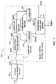
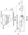
- FIG.2 there is shown a specific embodiment of a power detector, the basic power detector logic 200, in accordance with the invention.
- the power detector 200 accepts a power measurement signal p(t) produced by a power measurement stage 100 processing the receiver input signal y(t) .
- the said input signal y(t) consists of successive data bursts in a communication channel, said data bursts being separated by guard time intervals, where zero signal power has been emitted.
- the said processing stage 100 can be implemented in different ways as specified for example by prior art FIG.1b and FIG.1d.
- the signal p(t) undergo sampling at successive dates separated by a time interval T, producing the sampled signal p(n).
- This signal feeds the smoothing filter 210 producing a smoothed signal s(n).
- a comparator 240 compares the signal s(n) with a threshold THRESH0 producing a binary signal d1(n) at each date n.
- the signal d1(n) takes a value equal to " 1 " at date n if the signal s(n) is larger than THRESHO and equal to "0 " otherwise.
- An absolute derivative means 220 estimates the absolute value a(n) of the derivative of signal s(n) at each date n.
- a comparator 230 compares the signal a(n) with a threshold ATHRESH producing a binary signal d2(n) at each date n, where the signal d2(n) takes a value equal to " 0 " if the signal a(n) is larger than the threshold A THRESH and equal to " 1 " otherwise.
- a windowed logic-and means 250 coupled to receive as input the binary signals d1(n) and d2(n) and a binary signal w(n) produces the power detect signal r0(n) at each date n.
- the windowed logic-and means involves an and-gate coupled to receive as inputs the signals d1(n) and d2(n) producing a binary signal d(n) and a windowing function specified by the following truth table: d(n) w(n) r0(n) 0 X 0 1 1 1 1 0 r0(n-1) in which " X " signifies the don't care condition.
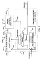
- FIG.3 there is shown another specific embodiment of a power detector in accordance with the invention.
- This power detector comprises three components: The first one is the basic power detector logic 200 accepting as input a power measurement signal p(t) , implementing the processing stages previously described with reference to FIG.2 in order to produce the binary signal r0(n) and the smoothed signal s(n) at successive dates n separated by a time interval T, wherein the threshold THRESHO can take a value THRESHO(n) at each date n.
- the said signal p(t) carries the power content of the receiver input signal y(t) , said signal y(t) consisting of successive data bursts in a communication channel, where a data burst extends over L consecutive dates separated by said time interval T . These data bursts are separated by guard time intervals, where a guard time interval extends over G consecutive dates.
- the second one is a frame control logic means 300 performing binary filtering coupled to receive as input the signal r0(n) producing as output a power detect signal r1(n) and two binary control signals e1(n) and e2(n).
- the signal r1(n) is produced by following the rules below:
- the said control signal e1(n) takes a value equal to " 1 " at date n if a " 0 " to “ 1 " transition is observed on the input signal r1(n) at two consecutive dates n-1 and n and it takes a " 0 " value otherwise.
- the said signal e2(n) takes a value equal to " 1 " at date n+G if a " 1 " to " 0 " transition is observed on the input signal r1(n) at two consecutive dates n-1 and n and it takes a "0” value otherwise.
- the third component is a threshold control logic means 310 coupled to receive as input the smoothed signal s(n) and the said control signals e1(n) and e2(n) producing the said threshold value THRESHO(n) at each date n.
- the threshold control logic means 310 comprises a maximum selection means 330 and a multiplexer means 340, where the maximum selection means 330 computes at each date n the maximum between the value of a threshold THRESH1 and the value of the expression s(n)-DTHRESH1, where DTHRESH1 is the value of certain threshold.
- the multiplexer means 340 receives as input the resulting signal max(n), along with signals el(n) and e2(n) and produces the said threshold value THRESHO(n) by setting the value of THRESHO(n) equal to the value of max(n) if the value of e1(n) is "1", setting the value of THRESHO(n) equal to the value of threshold THRESH1 if the value of e2(n) is "1" and maintaining at date n the value of THRESH0(n-1) at date n-1 otherwise.
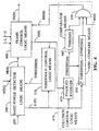
- FIG.4 there is shown another specific embodiment of a power detector in accordance with the invention.
- This power detector comprises four components: The first one is the Basic Power Detector Logic 200 accepting as input a signal p(t), implementing the processing stages previously described with reference to FIG.2 in order to produce the binary signal r0(n) and the smoothed signal s(n) at successive dates n separated by a time interval T, wherein the threshold THRESHO can take a value THRESHO(n) at each date n .
- the said signal p(t) carries the power content of the receiver input signal y(t) , said signal y(t) consisting of successive data bursts in a communication channel, where a data burst extends over L consecutive dates separated by said time interval T . These data bursts are separated by guard time intervals, where a guard time interval extends over G consecutive dates.
- the second one is a frame control logic means 400 performing a binary filtering coupled to receive as input the signal r0(n) and a binary signal int(n) producing as output a power detect signal rl(n) and two binary control signals e1(n) and e2(n).
- the signal r1(n) is the state label of a two-state finite state machine described as follows:
- SIPO serial-in parallel-out
- the preferred embodiment of the associated absolute derivative means 220 comprises a delay element 530 for delaying the said signal s(n) by D dates producing the delayed signal s(n-D), a subtractor 540 producing the difference of the input signal s(n) and the delayed version s(n-D) and absolute value extraction means 550 for evaluating the absolute value a(n) of the difference signal s(n)-s(n-D) at each date n.
Landscapes
- Physics & Mathematics (AREA)
- Electromagnetism (AREA)
- Engineering & Computer Science (AREA)
- Computer Networks & Wireless Communication (AREA)
- Signal Processing (AREA)
- Mobile Radio Communication Systems (AREA)
- Radio Relay Systems (AREA)
- Time-Division Multiplex Systems (AREA)
Applications Claiming Priority (2)
| Application Number | Priority Date | Filing Date | Title |
|---|---|---|---|
| GR99100230 | 1999-07-06 | ||
| GR99100230 | 1999-07-06 |
Publications (1)
| Publication Number | Publication Date |
|---|---|
| EP1069554A1 true EP1069554A1 (fr) | 2001-01-17 |
Family
ID=10943868
Family Applications (1)
| Application Number | Title | Priority Date | Filing Date |
|---|---|---|---|
| EP99600019A Withdrawn EP1069554A1 (fr) | 1999-07-06 | 1999-10-18 | Détecteur de puissance à gigue faible pour communications par accès multiple et à division dans le temps |
Country Status (2)
| Country | Link |
|---|---|
| EP (1) | EP1069554A1 (fr) |
| GR (1) | GR1003399B (fr) |
Cited By (3)
| Publication number | Priority date | Publication date | Assignee | Title |
|---|---|---|---|---|
| US7104534B2 (en) | 2001-06-08 | 2006-09-12 | Broadcom Corporation | System and method for detecting collisions in a shared communications medium |
| CN102394712A (zh) * | 2011-11-09 | 2012-03-28 | 南京邮电大学 | 认知无线电系统中检测周期与检测时间的联合优化方法 |
| CN108322655A (zh) * | 2015-06-12 | 2018-07-24 | 青岛海信电器股份有限公司 | 一种拍照方法 |
Citations (4)
| Publication number | Priority date | Publication date | Assignee | Title |
|---|---|---|---|---|
| EP0405610A2 (fr) * | 1989-06-30 | 1991-01-02 | Matsushita Electric Industrial Co., Ltd. | Méthode d'enregistrement d'information optique |
| US5373255A (en) * | 1993-07-28 | 1994-12-13 | Motorola, Inc. | Low-power, jitter-compensated phase locked loop and method therefor |
| EP0865035A2 (fr) * | 1997-03-14 | 1998-09-16 | Hitachi, Ltd. | Procédé d'enregistrement de signaux, circuit de détection de différence de phase et appareil de stockage d'informations |
| US5905767A (en) * | 1995-11-07 | 1999-05-18 | Mitsubishi Denki Kabushiki Kaisha | Timing recovery apparatus and a diversity communication apparatus using the same |
-
1999
- 1999-07-06 GR GR990100230A patent/GR1003399B/el not_active IP Right Cessation
- 1999-10-18 EP EP99600019A patent/EP1069554A1/fr not_active Withdrawn
Patent Citations (4)
| Publication number | Priority date | Publication date | Assignee | Title |
|---|---|---|---|---|
| EP0405610A2 (fr) * | 1989-06-30 | 1991-01-02 | Matsushita Electric Industrial Co., Ltd. | Méthode d'enregistrement d'information optique |
| US5373255A (en) * | 1993-07-28 | 1994-12-13 | Motorola, Inc. | Low-power, jitter-compensated phase locked loop and method therefor |
| US5905767A (en) * | 1995-11-07 | 1999-05-18 | Mitsubishi Denki Kabushiki Kaisha | Timing recovery apparatus and a diversity communication apparatus using the same |
| EP0865035A2 (fr) * | 1997-03-14 | 1998-09-16 | Hitachi, Ltd. | Procédé d'enregistrement de signaux, circuit de détection de différence de phase et appareil de stockage d'informations |
Cited By (5)
| Publication number | Priority date | Publication date | Assignee | Title |
|---|---|---|---|---|
| US7104534B2 (en) | 2001-06-08 | 2006-09-12 | Broadcom Corporation | System and method for detecting collisions in a shared communications medium |
| US7626996B2 (en) | 2001-06-08 | 2009-12-01 | Broadcom Corporation | System for detecting collisions in a shared communications medium |
| CN102394712A (zh) * | 2011-11-09 | 2012-03-28 | 南京邮电大学 | 认知无线电系统中检测周期与检测时间的联合优化方法 |
| CN102394712B (zh) * | 2011-11-09 | 2013-09-25 | 南京邮电大学 | 认知无线电系统中检测周期与检测时间的联合优化方法 |
| CN108322655A (zh) * | 2015-06-12 | 2018-07-24 | 青岛海信电器股份有限公司 | 一种拍照方法 |
Also Published As
| Publication number | Publication date |
|---|---|
| GR1003399B (el) | 2000-07-04 |
Similar Documents
| Publication | Publication Date | Title |
|---|---|---|
| US8331462B2 (en) | Method and apparatus for selective disregard of co-channel transmissions on a medium | |
| US8081104B2 (en) | Radar detection circuit for a WLAN transceiver | |
| US5748681A (en) | Offset correction for a homodyne radio | |
| EP0411756B1 (fr) | Récepteur pour radiotéléphone à commande de gain | |
| US20100253565A1 (en) | Method and apparatus to increase ADS-B squitter reception sensitivity | |
| EP0709975B1 (fr) | Procédé et appareil pour détection des bursts | |
| US20060199587A1 (en) | Radar detection circuit for a WLAN transceiver | |
| EP1683316B1 (fr) | Appareil de determination d'une erreur de decalage de frequence et recepteur correspondant | |
| US4017684A (en) | System for determining burst sending timing in TDMA communication | |
| EP0931391B1 (fr) | Synchronisation amelioree d'un recepteur avec un emetteur au moyen d'essais precoces/tardifs pendant la phase de synchronisation approximative | |
| US9602153B2 (en) | Radio receiving apparatus for receiving frequency-modulated radio signal | |
| US7835701B2 (en) | Detecting and eliminating spurious energy in communications systems via multi-channel processing | |
| JP3204224B2 (ja) | Dcオフセットのキャンセルとキャリア検出しきい値測定機能を備えた受信機とその制御方法 | |
| EP0430605B1 (fr) | Détecteur de fréquence basé sur une boucle de verrouillage de phase numérique | |
| EP1069554A1 (fr) | Détecteur de puissance à gigue faible pour communications par accès multiple et à division dans le temps | |
| US8259879B2 (en) | Method for detecting the eventual presence of an interferer, for example a radar signal, adapted to interfere with a wireless device, for example an UWB device, and corresponding device | |
| US5610950A (en) | Communication device with reduced sensitivity to in-channel interference | |
| US8036259B2 (en) | Interactive wireless communication device | |
| US6697613B1 (en) | System for canceling internal interference in a receiver | |
| CN116683941A (zh) | 一种雷达信号的检测方法、装置、电子设备及存储介质 | |
| EP1780915B1 (fr) | Procédé et dispositif permettant d'ignorer sélectivement des transmissions d'un même canal sur un support | |
| CN116193498B (zh) | 信道忙闲状态评估方法、装置和电子设备 | |
| JPH0653918A (ja) | 時分割多元接続通信の空きチャネル検出回路および方法 | |
| US5732108A (en) | Method and apparatus for producing a difference signal between two signal frequencies, and for detection of modulation | |
| JPH11234220A (ja) | 高周波信号検出装置 |
Legal Events
| Date | Code | Title | Description |
|---|---|---|---|
| PUAI | Public reference made under article 153(3) epc to a published international application that has entered the european phase |
Free format text: ORIGINAL CODE: 0009012 |
|
| AK | Designated contracting states |
Kind code of ref document: A1 Designated state(s): AT BE CH CY DE DK ES FI FR GB GR IE IT LI LU MC NL PT SE |
|
| AX | Request for extension of the european patent |
Free format text: AL;LT;LV;MK PAYMENT 19991105;RO PAYMENT 19991105;SI PAYMENT 19991105 |
|
| AKX | Designation fees paid |
Free format text: AT BE CH CY DE DK ES FI FR GB GR IE IT LI LU MC NL PT SE |
|
| AXX | Extension fees paid |
Free format text: MK PAYMENT 19991105;RO PAYMENT 19991105;SI PAYMENT 19991105 |
|
| 17P | Request for examination filed |
Effective date: 20010717 |
|
| STAA | Information on the status of an ep patent application or granted ep patent |
Free format text: STATUS: THE APPLICATION IS DEEMED TO BE WITHDRAWN |
|
| 18D | Application deemed to be withdrawn |
Effective date: 20050503 |