EP1067776A2 - Image display apparatus for fixing luminance of blank area and varying only luminance of image. - Google Patents
Image display apparatus for fixing luminance of blank area and varying only luminance of image. Download PDFInfo
- Publication number
- EP1067776A2 EP1067776A2 EP00304892A EP00304892A EP1067776A2 EP 1067776 A2 EP1067776 A2 EP 1067776A2 EP 00304892 A EP00304892 A EP 00304892A EP 00304892 A EP00304892 A EP 00304892A EP 1067776 A2 EP1067776 A2 EP 1067776A2
- Authority
- EP
- European Patent Office
- Prior art keywords
- image
- blank
- image display
- black level
- display apparatus
- Prior art date
- Legal status (The legal status is an assumption and is not a legal conclusion. Google has not performed a legal analysis and makes no representation as to the accuracy of the status listed.)
- Granted
Links
Images



Classifications
-
- H—ELECTRICITY
- H04—ELECTRIC COMMUNICATION TECHNIQUE
- H04N—PICTORIAL COMMUNICATION, e.g. TELEVISION
- H04N5/00—Details of television systems
- H04N5/14—Picture signal circuitry for video frequency region
- H04N5/20—Circuitry for controlling amplitude response
-
- H—ELECTRICITY
- H04—ELECTRIC COMMUNICATION TECHNIQUE
- H04N—PICTORIAL COMMUNICATION, e.g. TELEVISION
- H04N23/00—Cameras or camera modules comprising electronic image sensors; Control thereof
- H04N23/60—Control of cameras or camera modules
- H04N23/63—Control of cameras or camera modules by using electronic viewfinders
- H04N23/633—Control of cameras or camera modules by using electronic viewfinders for displaying additional information relating to control or operation of the camera
- H04N23/635—Region indicators; Field of view indicators
-
- H—ELECTRICITY
- H04—ELECTRIC COMMUNICATION TECHNIQUE
- H04N—PICTORIAL COMMUNICATION, e.g. TELEVISION
- H04N23/00—Cameras or camera modules comprising electronic image sensors; Control thereof
- H04N23/50—Constructional details
-
- H—ELECTRICITY
- H04—ELECTRIC COMMUNICATION TECHNIQUE
- H04N—PICTORIAL COMMUNICATION, e.g. TELEVISION
- H04N5/00—Details of television systems
- H04N5/14—Picture signal circuitry for video frequency region
- H04N5/16—Circuitry for reinsertion of DC and slowly varying components of signal; Circuitry for preservation of black or white level
-
- H—ELECTRICITY
- H04—ELECTRIC COMMUNICATION TECHNIQUE
- H04N—PICTORIAL COMMUNICATION, e.g. TELEVISION
- H04N5/00—Details of television systems
- H04N5/66—Transforming electric information into light information
Definitions
- the present invention relates to an image display apparatus.
- image display apparatuses include a function for adjusting the black level, that is, the level at which the luminance is lowest in an image to be displayed on a monitor of these apparatuses.
- a method is used to vary a ⁇ correction voltage in a ⁇ correction circuit.
- This ⁇ correction corrects the characteristics of gradation (degree of luminance variation) of an image to linear characteristics, and use of this correction also makes it possible to adjust the black level at which the luminance is lowest.
- a blank area is displayed on an image display apparatus such as that described above so that a blanking mark indicating a photographic range of a video camera, etc., is displayed superimposed on an image.
- This blank area is often displayed at the black level at which the luminance is lowest. It is preferable that the black level of this blank area always be at a predetermined level without being influenced by the luminance of an image to be displayed.
- An object of the present invention is to provide an image display apparatus capable of fixing the luminance of a blank area and varying only the luminance of an image.
- an image display apparatus comprising an A/D converter for converting an input analog image signal into digital image data; a black level setting unit for setting the black level of the digital image data by adjusting a lower-limit reference voltage of the A/D converter; a blank data generation unit for generating blank data for displaying a blank area around an image display area on a screen; an image data combining unit for combining blank data generated by this blank data generation unit and digital image data output from the A/D converter; and a display unit for displaying an output of this image data combining unit on the screen.
- the black level of an image display area can be adjusted by black level setting unit independently of the data of the blank area.
- the black level setting unit is a variable resistor.
- the black level setting unit preferably includes an illuminance sensor for detecting the illuminance of the surroundings of a video camera which outputs an analog image signal so that the black level is automatically set in correspondence with the illuminance of the surroundings of the camera.
- an image display apparatus 1 which is a programmable logic device (PLD), according to a first embodiment of the present invention is described below with reference to Fig. 1.
- the image display apparatus 1 is provided with input terminals 1a, 1b, and 1c for inputting a video signal from the outside.
- the image display apparatus 1 has contained therein a Y/C separation RGB decoding circuit 2, an A/D converter 3, a variable resistor 6, an image signal processing circuit 7, a gate driver 13, a source driver 14, a ⁇ correction circuit 15, a 6-inch high-resolution TFT LCD 16 having 962 ⁇ 562 pixels, a backlight 17, and an inverter 18.
- the input terminal 1a is connected to the input terminal of the Y/C separation RGB decoding circuit 2, and the output terminal of the Y/C separation RGB decoding circuit 2 is connected to the input terminal of the A/D converter 3.
- the input terminals 1b and 1c are connected directly to the input terminal of the A/D converter 3.
- the variable resistor 6 has three terminals, a second terminal thereof extending from the middle of the resistor so as to allow variation of the connection point with the resistor.
- the first and third terminals extend from both ends of the resistor. Therefore, the resistance value between the first terminal and the second terminal, and the resistance value between the second and the third terminal are variable.
- the second terminal is connected to the input terminal of the A/D converter 3.
- the first terminal is fixed to an upper-limit reference voltage Vh, and the third terminal is connected to a ground potential.
- the output terminal of the A/D converter 3 is connected to the input terminal of the image signal processing circuit 7.
- the output of this image signal processing circuit 7 is connected to the input terminals of the gate driver 13 and the source driver 14.
- the output terminal of the ⁇ correction circuit 15 is connected to the input terminal of the source driver 14.
- the output terminals of the gate driver 13 and the source driver 14 are connected to the input terminal of the LCD 16 so that each pixel of the LCD 16 is driven.
- the output terminal of the inverter 18 is connected to the input terminal of the backlight 17, and the inverter 18 drives the backlight 17.
- the backlight 17, disposed in the back of the LCD 16, emits transmission light which passes through this LCD 16 from the back of the LCD 16 so that this transmission light illuminates the LCD 16.
- the A/D converter 3 has contained therein a clamping circuit 4 and an A/D conversion circuit 5.
- the three input terminals provided in the A/D converter 3 are connected to the input terminal of the clamping circuit 4, and the output terminal of this clamping circuit 4 is connected to the input terminal of the A/D conversion circuit 5.
- the output terminal of the A/D conversion circuit 5 is connected to the output terminal of the A/D converter 3.
- the input terminal of the A/D converter 3, which is connected to the second terminal of the variable resistor 6, is connected to the input terminal of the lower-limit reference voltage of the A/D conversion circuit 5.
- the image signal processing circuit 7 has contained therein an image data conversion circuit 8, a blank data generation circuit 9, a blanking marker generation circuit 10, an image data combining circuit 11, and an LCD controller 12.
- the input terminal of the image signal processing circuit 7 is connected to the input terminal of the image data conversion circuit 8.
- the output terminals of the image data conversion circuit 8, the blank data generation circuit 9, and the blanking marker generation circuit 10 are connected to the input terminal of the image data combining circuit 11.
- the output terminal of the image data combining circuit 11 is connected to the input terminal of the LCD controller 12, and the output terminal of this LCD controller 12 is connected to the output terminal of the image signal processing circuit 7.
- a video signal from the input terminal of the image display apparatus 1 or from the output terminal of the Y/C separation RGB decoding circuit 2 is input to a terminal Vin of the A/D converter 3 through a capacitor 19.
- a clock signal is input to a terminal CLK of the A/D converter 3.
- a clamping pulse is input to a terminal CLP of the A/D converter 3.
- a clamping voltage is input to a terminal Vref of the A/D converter 3.
- the output terminal on the negative side of the reference voltage source 20 is connected to a ground potential.
- An 8-bit digital signal is output from the output terminals D0 to D7 of the A/D converter 3. This digital signal takes a digital value such that the section between the lower-limit reference voltage and the upper-limit reference voltage is divided evenly by 256, that is, an 8-bit digital value.
- a video signal which is an analog signal, is input from the input terminals 1a, 1b, or 1c provided in the image display apparatus 1.
- this video signal is input to the A/D converter 3 after passing through the Y/C separation RGB decoding circuit 2.
- the input video signal is input directly to the A/D converter 3.
- the black level that is, the level at which luminance is lowest, of the video signal which is input to the A/D converter 3 is clamped by the clamping circuit 4 contained in the A/D converter 3.
- the video signal whose black level is clamped, is digitized by the A/D conversion circuit 5.
- the digitized video signal is output from the A/D converter 3 and is input to the image signal processing circuit 7.
- the digitized video signal which is input to the image signal processing circuit 7, is converted into image data by the image data conversion circuit 8 contained in the image signal processing circuit 7, and is input to the image data combining circuit 11.
- Blank data output from the blank data generation circuit 9 contained also in the image signal processing circuit 7 is also input to the image data combining circuit 11.
- This blank data contains a signal which specifies a black level in a blank area on the screen.
- a blanking marker signal output from the blanking marker generation circuit 10 is also input to the image data combining circuit 11.
- This blanking marker signal contains a signal which specifies a white level (level at which the luminance is highest) of a boundary line between the image display area of the screen and the blank area thereof.
- the image data combining circuit 11 combines the image data, the blank data, and the blanking marker signal, and outputs the combined image data to the LCD controller 12.
- the LCD controller 12 converts the combined image data into an LCD driving signal and outputs the converted LCD driving signal to the gate driver 13 and the source driver 14.
- the LCD 16 is driven by the gate driver 13 and the source driver 14, and a combined image formed by the combined image data is displayed on the LCD 16.
- the ⁇ correction circuit 15 sends a ⁇ correction voltage to the source driver 14 so that ⁇ correction of the image is performed. Also, the inverter 18 drives the backlight 17 so that this backlight 17 supplies transmission illumination light from the back of the LCD 16.
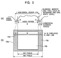
- a screen 16a of the LCD 16, shown at (b) in Fig. 3, is divided into an image display area 16b and a blank area 16c.
- the image display area 16b an image formed by the video signal input to the image display apparatus 1, that is, an image within the photographic range of a video camera or the like, is displayed.
- the blank area 16c a black level determined in accordance with blank data generated by the blank data generation circuit 9 is displayed.
- a waveform of combined image data (video signal) for displaying a particular line 16d in the horizontal direction on the screen 16a is shown at (a) in Fig. 3.
- one line in the horizontal direction is composed of 960 pixels, and among them, the number of pixels of the image display area 16b is 647.
- the blank area 16c is equally provided on the right and left of the image display area 16b.
- the line 16d is scanned from left to right.
- the blank area 16c is also equally provided in the upper and lower portions of the image display area 16b.
- a first interval A of the line 16d is drawn by an interval A' of a video signal, an interval B is drawn by an interval B', and an interval C is drawn by an interval C'.
- the signal level of the interval A' and the interval C' is a black level determined in accordance with the blank data generated by the blank data generation circuit 9.
- a blanking marker signal is inserted between the interval A' and the interval B' and between the interval B' and the interval C'.
- These blanking marker signals correspond to one pixel between the interval A and the interval B and between the interval B and the interval C in the line 16d on the screen 16a. Therefore, as a result of scanning by the line 16d being repeated, a white line is displayed vertically between the interval A and the interval B and between the interval B and the interval C on the screen 16a.
- the blank areas displayed in the upper and lower portions of the screen 16a are displayed by the line at this position by drawing the black level of the blank area over one horizontal period.
- the black level of the blank area 16c differs from the black level of the image display area 16b, each of which is determined by a mutually different signal. That is, the black level of the blank area 16c is determined by the blank data generated by the blank data generation circuit 9, and the black level of the image display area 16b is determined by the lower-limit reference voltage input to the terminal V1 of the A/D converter 3. This lower-limit reference voltage can be adjusted by the variable resistor 6.
- the blank data generated by the blank data generation circuit 9 does not pass through the A/D converter 3, even if the lower-limit reference voltage is changed, this blank data is not affected by this change. Therefore, even if the lower-limit reference voltage is adjusted by the variable resistor 6 and the black level of the image display area 16b is adjusted, the black level of the blank area 16c does not change.
- the black level (the level at which the luminance is lowest) of the input video signal is determined by the clamping voltage which has been input to the terminal Vref when a clamping pulse is input to the CLP terminal of the A/D converter 3.
- the digital signal output from the A/D converter 3 becomes a value determined by the relationship between the clamping voltage and the lower-limit reference voltage input to the terminal V1 of the A/D converter 3.
- the sampling of the video signal is performed in synchronization with the clock signal input to the terminal CLK of the A/D converter 3.
- a second embodiment of the present invention is described.
- the same components in Fig. 5 as those of the first embodiment are given the same reference numerals, and accordingly, descriptions thereof are omitted.
- an illuminance sensor 23 and a lower-limit reference voltage generation circuit 22 are provided.
- the illuminance sensor 23 is disposed, for example, near a video camera or the like which outputs a video signal to be input to the image display apparatus 1, and measures the illuminance near this video camera or the like.
- the output of the illuminance sensor 23 is input to the lower-limit reference voltage generation circuit 22, whereby a lower-limit reference voltage corresponding to this input Is output from the lower-limit reference voltage generation circuit 22, and this output is input to the A/D conversion circuit 5 inside the A/D converter 3.
- the lower-limit reference voltage automatically changes in accordance with the illuminance around the video camera or the like. Therefore, if the surroundings of the video camera or the like are bright, the lower-limit reference voltage also increases, and the black level of the signal also increases in accordance with this voltage. If, in contrast, the surroundings of the video camera are dark, the lower-limit reference voltage decreases, and the black level of the signal also decreases in accordance with this voltage.
- the black level of the blank area is determined only by the blank data output from the blank data generation circuit 9, and this blank data does not pass through the A/D conversion circuit 5 to which the lower-limit reference voltage is applied, even if the illuminance of the surroundings of the video camera or the like changes, this change is detected by the illuminance sensor 23, and the lower-limit reference voltage is changed as a result of this detection, the black level of the blank area does not change.
- the black levels of an image display area and a blank area can be set individually, even if the luminance of an image to be displayed is changed by adjusting the black level of the image display area, the black level of the blank area does not change.
Landscapes
- Engineering & Computer Science (AREA)
- Multimedia (AREA)
- Signal Processing (AREA)
- Liquid Crystal Display Device Control (AREA)
- Control Of Indicators Other Than Cathode Ray Tubes (AREA)
- Controls And Circuits For Display Device (AREA)
- Transforming Electric Information Into Light Information (AREA)
- Studio Devices (AREA)
- Liquid Crystal (AREA)
- Picture Signal Circuits (AREA)
- Image Processing (AREA)
- Television Receiver Circuits (AREA)
Abstract
Description
Claims (4)
- An image display apparatus comprising:A/D conversion means for converting an input analog image signal into digital image data;black level setting means for setting the black level of the digital image data by adjusting a lower-limit reference voltage of the A/D conversion means;blank data generation means for generating blank data for displaying a blank area around an image display area on a screen;image data combining means for combining blank data generated by this blank data generation means and digital image data output from said A/D conversion means; anddisplay means for displaying the output of this image data combining means on said screen.
- An image display apparatus according to claim 1, wherein said black level setting means is a variable resistor.
- An image display apparatus according to claim 1, wherein said black level setting means comprises an illuminance sensor for detecting the illuminance around a video camera which outputs said analog image signal.
- An image display apparatus according to claim 3, wherein said black level setting means outputs a lower-limit reference voltage corresponding to illuminance detected by said illuminance sensor.
Applications Claiming Priority (2)
| Application Number | Priority Date | Filing Date | Title |
|---|---|---|---|
| JP11190996A JP2001022331A (en) | 1999-07-05 | 1999-07-05 | Image display device |
| JP19099699 | 1999-07-05 |
Publications (3)
| Publication Number | Publication Date |
|---|---|
| EP1067776A2 true EP1067776A2 (en) | 2001-01-10 |
| EP1067776A3 EP1067776A3 (en) | 2004-03-17 |
| EP1067776B1 EP1067776B1 (en) | 2007-11-07 |
Family
ID=16267139
Family Applications (1)
| Application Number | Title | Priority Date | Filing Date |
|---|---|---|---|
| EP00304892A Expired - Lifetime EP1067776B1 (en) | 1999-07-05 | 2000-06-09 | Image display apparatus for fixing luminance of blank area and varying only luminance of image. |
Country Status (3)
| Country | Link |
|---|---|
| EP (1) | EP1067776B1 (en) |
| JP (1) | JP2001022331A (en) |
| DE (1) | DE60036984T2 (en) |
Families Citing this family (3)
| Publication number | Priority date | Publication date | Assignee | Title |
|---|---|---|---|---|
| KR100369822B1 (en) * | 2000-12-22 | 2003-01-30 | 삼성전자 주식회사 | Display Apparatus and Method Controlling the Same |
| KR101183399B1 (en) | 2006-03-31 | 2012-09-14 | 엘지디스플레이 주식회사 | Display and Driving Method thereof |
| US8290293B2 (en) * | 2006-10-17 | 2012-10-16 | Samsung Electronics Co., Ltd. | Image compensation in regions of low image contrast |
Family Cites Families (10)
| Publication number | Priority date | Publication date | Assignee | Title |
|---|---|---|---|---|
| US4065790A (en) * | 1976-11-17 | 1977-12-27 | Eric Siegel | Video processing amplifier providing black level correction |
| US4527201A (en) * | 1983-03-29 | 1985-07-02 | Panavision, Inc. | Zoom indicating apparatus for video camera or the like |
| JPH0346632Y2 (en) * | 1985-03-30 | 1991-10-02 | ||
| US4628362A (en) * | 1985-05-02 | 1986-12-09 | American Dynamics Corporation | Combined video AGC and digitizing circuit |
| JPH04172066A (en) * | 1990-11-06 | 1992-06-19 | Hitachi Ltd | Video camera |
| JP3211969B2 (en) * | 1991-06-27 | 2001-09-25 | ソニー株式会社 | Display device |
| JP3221967B2 (en) * | 1993-03-31 | 2001-10-22 | 富士写真フイルム株式会社 | Imaging device |
| JP3291843B2 (en) * | 1993-07-05 | 2002-06-17 | ソニー株式会社 | Video signal black level playback device |
| CA2253820C (en) * | 1996-05-06 | 2007-10-23 | Cimatrix | Smart progressive-scan charge-coupled device camera |
| JP3277984B2 (en) * | 1997-03-31 | 2002-04-22 | 日本電気株式会社 | Video signal processing device |
-
1999
- 1999-07-05 JP JP11190996A patent/JP2001022331A/en not_active Withdrawn
-
2000
- 2000-06-09 EP EP00304892A patent/EP1067776B1/en not_active Expired - Lifetime
- 2000-06-09 DE DE60036984T patent/DE60036984T2/en not_active Expired - Fee Related
Also Published As
| Publication number | Publication date |
|---|---|
| EP1067776B1 (en) | 2007-11-07 |
| JP2001022331A (en) | 2001-01-26 |
| DE60036984T2 (en) | 2008-08-28 |
| DE60036984D1 (en) | 2007-12-20 |
| EP1067776A3 (en) | 2004-03-17 |
Similar Documents
| Publication | Publication Date | Title |
|---|---|---|
| KR100806903B1 (en) | Liquid crystal display and driving method thereof | |
| US7893907B2 (en) | Method and apparatus for driving liquid crystal display | |
| EP2105912A3 (en) | Drive circuit for display device with uniform luminance characteristics | |
| US8508556B2 (en) | Image display method | |
| US6292269B1 (en) | Method and apparatus for image reading capable of detecting dust that disturbs image reading operation | |
| US20090096819A1 (en) | Driving circuit apparatus | |
| EP0825584A3 (en) | Driving method and circuit for an array of display cells or light valves | |
| KR20080045900A (en) | LCD and its driving method | |
| KR20020092075A (en) | Liquid crystal display with an adjusting function of a gamma curve | |
| TWI383371B (en) | Timing controller, display device and method for adjusting gamma voltage | |
| US20060139272A1 (en) | Gamma voltage generating apparatus and method of testing a gamma voltage | |
| US7002605B1 (en) | Image display apparatus for fixing luminance of blank area and varying only luminance of image | |
| JP2002372960A (en) | Method and circuit for reducing sparkle artifacts with low brightness filtering | |
| KR100298265B1 (en) | Vision-dependent characteristic correction circuit, correction method and display device | |
| EP1067776B1 (en) | Image display apparatus for fixing luminance of blank area and varying only luminance of image. | |
| JP2005502091A (en) | Liquid crystal display device with inversion flicker compensation | |
| US20070290969A1 (en) | Output buffer for gray-scale voltage source | |
| KR100487309B1 (en) | Apparatus and for Adjusting Gamma and White Balance of LCD Projection TV and Method of The Same | |
| CN101510400B (en) | Driving system for liquid crystal display device, liquid crystal display device including the same, and driving method using the same | |
| KR20170030144A (en) | Display apparatus and method of driving the same | |
| JPH05236400A (en) | Liquid crystal display device | |
| JPH0594156A (en) | Liquid crystal display | |
| JP2004117598A (en) | Method for driving liquid crystal panel, liquid crystal display device, and monitor | |
| US20070085799A1 (en) | Liquid crystal display apparatus, device of drivng the same and method of driving the same | |
| JP4889397B2 (en) | Voltage converter |
Legal Events
| Date | Code | Title | Description |
|---|---|---|---|
| PUAI | Public reference made under article 153(3) epc to a published international application that has entered the european phase |
Free format text: ORIGINAL CODE: 0009012 |
|
| AK | Designated contracting states |
Kind code of ref document: A2 Designated state(s): AT BE CH CY DE DK ES FI FR GB GR IE IT LI LU MC NL PT SE |
|
| AX | Request for extension of the european patent |
Free format text: AL;LT;LV;MK;RO;SI |
|
| PUAL | Search report despatched |
Free format text: ORIGINAL CODE: 0009013 |
|
| AK | Designated contracting states |
Kind code of ref document: A3 Designated state(s): AT BE CH CY DE DK ES FI FR GB GR IE IT LI LU MC NL PT SE |
|
| AX | Request for extension of the european patent |
Extension state: AL LT LV MK RO SI |
|
| RIC1 | Information provided on ipc code assigned before grant |
Ipc: 7H 04N 5/20 A Ipc: 7H 04N 5/232 B |
|
| 17P | Request for examination filed |
Effective date: 20040503 |
|
| AKX | Designation fees paid |
Designated state(s): DE FR GB NL |
|
| 17Q | First examination report despatched |
Effective date: 20070115 |
|
| GRAP | Despatch of communication of intention to grant a patent |
Free format text: ORIGINAL CODE: EPIDOSNIGR1 |
|
| GRAS | Grant fee paid |
Free format text: ORIGINAL CODE: EPIDOSNIGR3 |
|
| GRAA | (expected) grant |
Free format text: ORIGINAL CODE: 0009210 |
|
| AK | Designated contracting states |
Kind code of ref document: B1 Designated state(s): DE FR GB NL |
|
| REG | Reference to a national code |
Ref country code: GB Ref legal event code: FG4D |
|
| REF | Corresponds to: |
Ref document number: 60036984 Country of ref document: DE Date of ref document: 20071220 Kind code of ref document: P |
|
| PG25 | Lapsed in a contracting state [announced via postgrant information from national office to epo] |
Ref country code: NL Free format text: LAPSE BECAUSE OF FAILURE TO SUBMIT A TRANSLATION OF THE DESCRIPTION OR TO PAY THE FEE WITHIN THE PRESCRIBED TIME-LIMIT Effective date: 20071107 |
|
| NLV1 | Nl: lapsed or annulled due to failure to fulfill the requirements of art. 29p and 29m of the patents act | ||
| EN | Fr: translation not filed | ||
| PLBE | No opposition filed within time limit |
Free format text: ORIGINAL CODE: 0009261 |
|
| STAA | Information on the status of an ep patent application or granted ep patent |
Free format text: STATUS: NO OPPOSITION FILED WITHIN TIME LIMIT |
|
| 26N | No opposition filed |
Effective date: 20080808 |
|
| PG25 | Lapsed in a contracting state [announced via postgrant information from national office to epo] |
Ref country code: FR Free format text: LAPSE BECAUSE OF FAILURE TO SUBMIT A TRANSLATION OF THE DESCRIPTION OR TO PAY THE FEE WITHIN THE PRESCRIBED TIME-LIMIT Effective date: 20080822 |
|
| PGFP | Annual fee paid to national office [announced via postgrant information from national office to epo] |
Ref country code: GB Payment date: 20090507 Year of fee payment: 10 Ref country code: DE Payment date: 20090630 Year of fee payment: 10 |
|
| GBPC | Gb: european patent ceased through non-payment of renewal fee |
Effective date: 20100609 |
|
| PG25 | Lapsed in a contracting state [announced via postgrant information from national office to epo] |
Ref country code: DE Free format text: LAPSE BECAUSE OF NON-PAYMENT OF DUE FEES Effective date: 20110101 |
|
| PG25 | Lapsed in a contracting state [announced via postgrant information from national office to epo] |
Ref country code: GB Free format text: LAPSE BECAUSE OF NON-PAYMENT OF DUE FEES Effective date: 20100609 |