EP1067775A2 - Digitale Bildaufnahmesteuerung mit selektiver Erhöhung des Dynamikbereichs - Google Patents
Digitale Bildaufnahmesteuerung mit selektiver Erhöhung des Dynamikbereichs Download PDFInfo
- Publication number
- EP1067775A2 EP1067775A2 EP00302086A EP00302086A EP1067775A2 EP 1067775 A2 EP1067775 A2 EP 1067775A2 EP 00302086 A EP00302086 A EP 00302086A EP 00302086 A EP00302086 A EP 00302086A EP 1067775 A2 EP1067775 A2 EP 1067775A2
- Authority
- EP
- European Patent Office
- Prior art keywords
- signal
- value
- luminance
- adc
- image
- Prior art date
- Legal status (The legal status is an assumption and is not a legal conclusion. Google has not performed a legal analysis and makes no representation as to the accuracy of the status listed.)
- Withdrawn
Links
- 238000003384 imaging method Methods 0.000 title abstract description 23
- 238000012545 processing Methods 0.000 claims description 39
- 238000000034 method Methods 0.000 claims description 33
- 239000013643 reference control Substances 0.000 claims description 6
- 230000004044 response Effects 0.000 claims description 5
- 230000010354 integration Effects 0.000 abstract description 41
- 238000001228 spectrum Methods 0.000 abstract description 12
- 230000000875 corresponding effect Effects 0.000 description 15
- 230000003287 optical effect Effects 0.000 description 14
- 230000008569 process Effects 0.000 description 9
- 230000008901 benefit Effects 0.000 description 3
- 230000002596 correlated effect Effects 0.000 description 3
- 238000010586 diagram Methods 0.000 description 3
- 238000001914 filtration Methods 0.000 description 3
- 238000012986 modification Methods 0.000 description 3
- 230000004048 modification Effects 0.000 description 3
- 238000005070 sampling Methods 0.000 description 3
- 241001085205 Prenanthella exigua Species 0.000 description 2
- 230000001276 controlling effect Effects 0.000 description 2
- 238000012937 correction Methods 0.000 description 2
- 230000006870 function Effects 0.000 description 2
- 238000007689 inspection Methods 0.000 description 2
- 238000004519 manufacturing process Methods 0.000 description 2
- 238000012360 testing method Methods 0.000 description 2
- 238000012546 transfer Methods 0.000 description 2
- 238000004364 calculation method Methods 0.000 description 1
- 230000008859 change Effects 0.000 description 1
- 230000002950 deficient Effects 0.000 description 1
- 238000013461 design Methods 0.000 description 1
- 238000005516 engineering process Methods 0.000 description 1
- 230000006872 improvement Effects 0.000 description 1
- 230000000977 initiatory effect Effects 0.000 description 1
- 230000007246 mechanism Effects 0.000 description 1
- 230000003068 static effect Effects 0.000 description 1
Images


Classifications
-
- H—ELECTRICITY
- H04—ELECTRIC COMMUNICATION TECHNIQUE
- H04N—PICTORIAL COMMUNICATION, e.g. TELEVISION
- H04N5/00—Details of television systems
- H04N5/14—Picture signal circuitry for video frequency region
- H04N5/16—Circuitry for reinsertion of DC and slowly varying components of signal; Circuitry for preservation of black or white level
-
- H—ELECTRICITY
- H04—ELECTRIC COMMUNICATION TECHNIQUE
- H04N—PICTORIAL COMMUNICATION, e.g. TELEVISION
- H04N23/00—Cameras or camera modules comprising electronic image sensors; Control thereof
- H04N23/70—Circuitry for compensating brightness variation in the scene
- H04N23/76—Circuitry for compensating brightness variation in the scene by influencing the image signals
-
- H—ELECTRICITY
- H04—ELECTRIC COMMUNICATION TECHNIQUE
- H04N—PICTORIAL COMMUNICATION, e.g. TELEVISION
- H04N25/00—Circuitry of solid-state image sensors [SSIS]; Control thereof
- H04N25/60—Noise processing, e.g. detecting, correcting, reducing or removing noise
- H04N25/68—Noise processing, e.g. detecting, correcting, reducing or removing noise applied to defects
- H04N25/683—Noise processing, e.g. detecting, correcting, reducing or removing noise applied to defects by defect estimation performed on the scene signal, e.g. real time or on the fly detection
-
- H—ELECTRICITY
- H04—ELECTRIC COMMUNICATION TECHNIQUE
- H04N—PICTORIAL COMMUNICATION, e.g. TELEVISION
- H04N5/00—Details of television systems
- H04N5/14—Picture signal circuitry for video frequency region
- H04N5/20—Circuitry for controlling amplitude response
Definitions
- This invention relates generally to digital imaging devices and specifically to automatic and selective intensity resolution enhancement of a digital image.
- An image consists of an array of picture elements and those picture elements are referred to in the following description as pixels.
- Digital imaging devices are becoming increasingly popular in a variety of applications, including digital cameras, fingerprint recognition, digital scanners and copiers, and the like.
- Typical prior art digital imaging devices are based on charge coupled device (CCD) technology.
- CCD devices have an array of CCD cells, each cell comprising a pixel.
- Each CCD pixel outputs a voltage signal in proportion to the intensity of light impinging upon the cell.
- This analog voltage signal can be converted to a digital signal for further processing, digital filtering, storage and the like.
- a two dimensional digital image can be constructed from the voltage signals output from a two-dimensional array of CCD cells, commonly referred to as a sensor array.
- the resulting image may have poor resolution. Poor image resolution could result from very bright light impinging upon sensor array, in which case the resulting image might appear washed out, or low light conditions, in which case the resulting image might appear dark and indistinct. Another contributor to poor image quality might be insufficient contrast between light and dark pixels, resulting in a blurred or faded image. While digital signal processing may be employed to compensate for certain image quality problems, considerable image improvement can be obtained by adjusting how the analog voltage signal coming from the sensor array is handled prior to being input to the analog to digital converter.
- a common technique for improving image resolution is to increase the contrast lighting conditions.
- the present invention provides a method of controlling a luminance signal in an image-processing device including the steps of:
- the present invention provides a method of automatic gain control in an image processor including an amplifier provided with a reference signal input port, a signal input port and an output port, the gain of the amplifier being adjustable, and an analog to digital converter including an input port connected to the output port of the amplifier and an output port for providing a digital code corresponding to the output value from the amplifier,
- the invention also provides a means for controlling a luminance signal in an image-processing device including:
- the present invention may be included in an automatic gain control circuit comprising:
- An embodiment of the present invention is an image processor comprising:
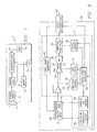
- FIG. 1 illustrates a digital imaging device 2 utilizing preferred embodiments of the present invention.
- the digital imaging device includes a lens mechanism 4 which receives light emanating or reflected from an object to be imaged and focuses the incoming light upon an array sensor 6.
- the array sensor 6 is preferably a CMOS sensor array of the type fully described in co-pending patent application 09/223,166, entitled Fast Frame Readout Architecture for Array Sensors with Integrated Correlated Double Sampling System, which application is incorporated herein by reference.
- the sensor array 6 is comprised of a two dimensional array of CMOS sensors, each sensor corresponding to a pixel of the resulting image.
- Each sensor outputs an analog voltage signal, which signal is in proportion to the intensity of light impinging upon the particular sensor.
- the voltage signal from each sensor can be scanned in a raster format as is well known in the art to generate an analog image signal.
- This analog image signal is fed to imaging logic 8 where the analog signal is buffered and amplified before being converted to a digital signal.
- the digital signal can be filtered or further processed before being passed to an input / output (IO) port 10 in the form of pixel intensity data.
- IO input / output
- the digital signal can be output in the form of a bitmap or other well known digital picture format.
- the digital signal can be passed to a memory 12 for storage.
- the memory 12 is preferably a dynamic random access memory or a static random access memory.
- the memory 12 could be a magnetic or optical storage device, such as a magnetic diskette device, a CD-ROM, or other storage device. In each case, an appropriate device controller and interface (not shown) would be included along with the memory 12.
- the imaging logic 8, memory 12, and I/O port 10 are preferably under the control of a microprocessor 14, which is preferably a general purpose digital microprocessor operating under instructions stored in the memory 12 or a ROM 16. Stored instructions could also be provided via the I/O port 10 directly to the microprocessor 14, or stored in the memory 12 or the ROM 16.
- the sensor array 6 is formed of an array of CMOS sensor cells, thus allowing for the imaging logic 8 to be formed using CMOS processes on a single integrated circuit along with the sensor array 6.
- Figure 2 illustrates a single integrated circuit (IC) 20, upon which is realized both the sensor array 6 and the imaging logic 8 according to the preferred embodiment of the invention.
- IC integrated circuit
- Other features and circuits may be included within the IC 20 including internal control registers, microprocessor interface logic, memory interface logic, and the like. These features have not been illustrated as they are not necessary for an understanding of the present invention.
- the details of the imaging logic 8 will now be described with reference to Figure 2.
- the main path for imaging signals is indicated by heavy arrows.
- the analog signal from the sensor array 6 is passed to a buffer 22 where the signal is strengthened and fixed pattern noise is removed.
- the buffered analog signal is sent to a first input of a programmable gain differential amplifier 24.
- the second input of the amplifier 24 receives a reference voltage, which is fed from a reference control block 26 under the control of a digital signal controller 28.
- the amplifier 24 also receives a gain control signal from a gain control block 30, which operates under the control of a digital signal controller 28.
- the amplifier 24 maps the two inputs to a fully differential output 25, 27.
- the outputs 25 and 27 correspond to the difference between the value of the two input signals (i.e. the analog image signal and the reference voltage V REF ) multiplied by the gain of the amplifier 24 and centered about a common mode voltage level.
- This fully differential output 25, 27 is then fed to the inputs of a differential analog to digital converter (ADC) 32 where the differential value (i.e. the difference between signals 25 and 27) is converted to a digital value.
- ADC analog to digital converter
- the resulting digital image signal is then passed to a defective-pixel filter 34 where image errors are detected and corrected, as described in detail in co-pending patent application 09/223,165, entitled Sequential Correlated Double Sampling Technique for CMOS Area Array Sensors, which application is incorporated herein by reference.
- the corrected digital image signal is then passed to a digital micro-interface 36 which provides an interface between the IC 20 and other components of the digital imager 2, such as the memory 12, microprocessor 14 or I/O port 10.
- the processing of the image signal for luminance control involves the generation of an average value of the image signal by means of a digital average calculator 38 and it will be appreciated that the average value of the image signal without correction is substantially the same as the average value after correction by the defective-pixel filter 34.
- a digital timing generator 42 which provides timing signals for operation of a sequential correlated doubling sampling block 44 in order to suppress CMOS sensor fixed pattern noise.
- a row / column information register 46 provides information to the digital signal controller 28 and the digital average calculator 38 regarding where the signal currently being processed originated on the sensor array (i.e. provides row and column information for each pixel).
- the imaging logic 8 also includes a digital signal feedback loop comprising the digital average calculator 38, digital signal controller 28, reference control block 26, gain control block 30 and exposure time control 40.
- This feedback loop is employed to optimize the output of the amplifier 24 so as to take advantage of the fully dynamic range of the analog to digital converter (ADC) 32. This is accomplished by adjusting either the gain of amplifier 24 or the reference voltage V REF input or both.
- ADC analog to digital converter
- Two separate aspects of the image are optimized: optical black calibration ensures that optically black pixels result in a near zero value being output from the ADC 32, while ensuring that the full dynamic range of the ADC 32 is utilized; and resolution enhancement provides for optimum contrast in the image.
- image resolution is accomplished automatically via the feedback loop.
- a user can select certain values to enhance the image or a portion of the image-dynamic-range of interest to the user, as will be explained in more detail below.
- Optical black calibration is accomplished by detecting a signal from pixels (i.e. CMOS sensors) that are known to be "dark,” i.e. receiving no light impinging upon them. This is accomplished by the use of a light shield 48 over a portion of the sensor array 6.
- the light shield 48 covers the first four rows of pixels, although the number of shielded pixels and rows is a matter of design choice. Because these rows are known to be dark, the imaging logic can be calibrated to treat these pixels as black, i.e. to have a minimum digital value associated with them. For reasons that will become apparent, this minimum digital value should not be set to zero. In the preferred embodiment, the minimum digital value, corresponding to fully black or a fully dark pixel, is set to 64.
- the reference voltage V REF input to the amplifier 24 is adjusted in order to drive the output of the ADC 32 to its "black" value, preferably 64.
- the relationships between V REF and the output of the ADC 32 will be described with reference to Figure 3, which illustrates the relationship between the amplifier 24, ADC 32, and reference control block 26.
- the amplifier 24 receives as input the pixel intensity signal, V sig on its non-inverting input and the reference voltage signal V REF on its inverting input. The amplifier 24 then outputs a differential signal which is equivalent to the difference between the inputs multiplied by the gain.
- the amplifier 24 is configured such that the differential output signal 25, 27 is centered about the common mode level (CML) 29 of the differential ADC 32.
- CML common mode level
- the amplifier 24 maps the difference between its input signals to a differential signal centered about CML.
- the maximum and minimum operating thresholds of the ADC 32 are referred to as V T and V B respectively, and the CML level 29 is midway between V T and V B .
- g the gain of the amplifier 24.
- g 1, although the amplifier 24 is preferably programmable with a gain value of 2, 4, 8, or 16.
- V inp CML + (V inp - V inm )/2.
- D outn (V inp - V B )/ / (V T - V B ).
- Equation 4 can be employed to force the value D outn to the desired level 64 for a given pixel signal V sig and for a constant gain g, by adjusting the reference voltage input V REF to the amplifier 24. As the known black pixels corresponding to the pixels beneath shield 48 are being scanned, the appropriate value for V REF is derived.
- the reference control block 26 includes a variable voltage source 52 and a digital to analog converter (DAC) 54.
- the DAC 54 receives a digital signal and converts it into an analog signal which feeds a variable voltage source 52, from which the reference voltage input V REF is generated.
- the relationship between the normalized output D outn of the ADC 32 and the input D inm is given as follows.
- V REF D inm * (VT DAC - VB DAC ) / (2 m - 1)
- D inm is the digital input to the DAC 54
- VT DAC is the top reference for the DAC 54
- VB DAC is the bottom reference for the DAC 54.
- the ADC 32 is ten bits wide and the DAC 54 is eight bits wide, resulting in the approximation: delta(D inm ) ⁇ -delta(D outn )/ 2*g.
- equation 9 allows for fast computation of the required input to the DAC 54 in order to generate the required reference voltage V REF for optical black calibration.
- the process begins with the initiation of a new frame at step 60.
- decision step 62 the output D out of the ADC 32 for a known optically black pixel (i.e. a pixel that is shielded by the shield 48) is compared to a threshold value or a threshold range to determine if the output is within the acceptable range for an optically black pixel.
- the ADC 32 will output a value of 64 for such a pixel, with a range of plus or minus 10 being allowed.
- step 64 If the output is within the allowed range, then there is no need to adjust the reference voltage V REF input to the amplifier 24, so the value for V REF is frozen, as indicated by step 64, and processing proceeds to decision step 68. If, on the other hand, the output of the ADC 32 is not within the allowed range, then processing proceeds to step 66 where the value for V REF is adjusted in order to drive the output of the ADC 32 to the value 64, as discussed above with reference to equations 4 and 9. Processing then proceeds to decision step 68 where it is determined whether the row being scanned is still within the optical black region. In the preferred embodiments, the shield 48 blacks out the first four rows of pixels and information from the row / column information register 46 indicates whether the row being scanned is from one of the blacked out rows.
- step 69 V REF is frozen and the remainder of the frame rows are scanned and analyzed, until the end of the frame is reached, as indicated by decision step 70.
- step 72 V REF is once again adjusted. This time, however, V REF is adjusted, in order to match the characteristics of the entire frame that was just scanned, rather than trying to optimize the optical black value.
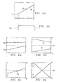
- Figure 5a plots the luminance values for a frame over time.
- Figure 5b provides the time chart for V REF during the scan of one frame.
- the frame shown in 5a is for illustration only and represents a test pattern in which the first four rows of pixels are blacked out (as shown by the flat portion of luminance curve 76) and then the remaining rows increase from black to bright white as the scan proceeds down the frame (as shown by the sloping portion of luminance curve 76).
- the luminance intensity would vary widely and nonlinearly, but the principles described herein would apply equally.
- the value for V REF is initially set to some default value, preferably the common mode level of the ADC 32. After the first four rows have been scanned, a new value for V REF is calculated in step 66 of Figure 4 and as indicated by the change in the value of V REF at time t 1 . Alternatively, the value of V REF could be updated after each pixel in the blacked out rows is scanned or at the end of each of the blacked out rows. Note that the latency between the end of the blacked out rows and the calculation of the value for V REF is preferably minimized by the use of the fast computation allowed by equation 9, and because of the use of fast computational logic 8 on the same chip as the sensor array 6. Once the value for V REF is determined for the optical black pixels, this value is frozen (step 61 of Figure 4) and the remainder of the frame is scanned, as indicated between times T 1 and T 2 .
- V REF is calculated based upon the actual frame data.
- the average luminance value for the frame is first calculated. This value is introduced for the value of V sig in equation 4 and V REF is adjusted in order to drive the output of the ADC 32 to its mid-range value. For a preferred ten bit ADC, this mid-range value might be set to 512.
- the mid-range ADC output value D out is preferably a programmable value that can be selected according to the image being scanned and the user's preferences. Empirical evidence suggests that the ADC output value corresponding to the average luminance intensity 78 should be set to about the 75% point of the ADC's range (say 768 for a ten bit ADC) for best image enhancement.
- V REF is adjusted at the end of the frame (step 72 of Figure 4) and processing repeats for the next incoming frame of luminance data.
- the gain of the amplifier 24 is also adjusted in order to try to maximize the dynamic range of the ADC 32. This is explained in more detail in the following paragraphs.
- FIG. 6a shows the inputs to the amplifier 24 for the scan of one entire frame.
- Figure 6b illustrates the corresponding differential output 25, 27 from the amplifier 24.
- V REF is illustrated as having already been adjusted for optical black calibration at the end of the first four rows.
- the lower component 27 of the differential output signal is at or very near the lower threshold V B of the ADC 32 as indicated.
- the differential output signal 25, 27 does not utilize the full range of ADC 32.
- its inputs in this case differential output 25, 27 from the amplifier 24
- its inputs in this case differential output 25, 27 from the amplifier 24
- V B to V T In this way, the contrast of the resulting image is enhanced.
- the average luminance value for the frame is calculated.
- This average brightness value 80 is shown in Figure 6c, which again illustrates the differential output 25, 27 of the amplifier 24.
- V REF can be adjusted such that the output of the amplifier 24 will drive the ADC 32 to its mid-point range for an incoming luminance value V sig equivalent to the average brightness value.
- the differential output signal 25, 27 is shown as having been shifted up in order to put the average brightness value at the common mode level, or mid-range level of the ADC 32 (for clarity only one component 27 of the differential output signal 25, 27 is illustrated) .
- the differential output signal 25, 27 will be shifted up in order to bring the average brightness value to about 75% of V T .
- the brighter portions of the image which are typically the areas of most interest, will be enhanced.
- the average brightness value could be shifted to anywhere within the range of the ADC 32. This variability is accomplished by the use of user programmable registers. Note that Figure 6c is illustrative only and does not correspond to actual output signals from the amplifier 24. The drawing merely illustrates the intended result (for the next frame of data) of adjusting V REF after the first frame has been read.
- the differential output signal 25, 27 is expanded to extend across the full range of the ADC 32 (or as much is practical) by increasing the gain of the amplifier 24. This increase in gain will adjust the slope of the differential output 25, 27, as shown in Figure 6d. Figure 7 provides additional details regarding the gain adjustment.
- Figure 7a is a flow chart illustrating the method of adjusting the gain of the amplifier 24 in order to match its differential output 25, 27 to the range of the ADC 32 for the luminance signal of the last scanned frame. It is expected that the next frame will be similar in luminance values and hence its contrast will be improved by using the gain calculated for the immediately preceding frame.
- a first decision step 90 it is determined whether a chip reset has occurred. If so, the process proceeds to step 92 where a gain factor gain is set to a value stored in a register or other memory source.
- the gain factor is a three bit value, i.e. 0 through 7, that corresponds to the gain of the amplifier 24 as shown in Figure 3b.
- the amplifier 24 can impose a gain of 1X, 2X, 4X, 8X, or 16X. If a chip reset has not occurred, the process proceeds to step 94 where it is determined whether the imaging logic is operating in user controlled mode, i.e. the automatic image enhancement features have been disabled. In that case, processing proceeds to step 92 where the gain factor is set to a value stored in a register or other memory source. Note that the value can be a pre-programmed default value or can be a value input by the user of the system.
- processing continues to decision step 96 where it is determined whether the automatic gain control feature has been temporarily disabled by the system to allow the system time to stabilize after the integration interval has been adjusted. If so, the gain factor is not changed and processing discontinues, as shown in block 98. If automatic gain control is enabled, processing continues to decision step 100 where it is determined if an entire frame has been scanned. If not, the gain factor is unchanged, as shown in step 102. If the end of the frame has been reached, as may be indicated by an end of frame signal from the Row / Column Information Register 45, the processing proceeds to decision step 104 where the average brightness value is calculated. This average brightness value is then compared to a pre-set threshold value. As discussed above, this pre-set threshold value could correspond to the mid-range of the ADC 32 or more preferably to the 75% range.
- step 104 it is determined whether the gain factor is less than or equal to two, corresponding to the minimum gain value of 2X. If the gain factor is greater than 2, indicating that the gain of the amplifier 24 can be adjusted down, processing continues to step 108 where the gain factor is decremented by one. By reference to Figure 7b it is seen that decrementing the gain factor will cause the gain of the amplifier 24 to be cut in half (assuming the gain factor is at 3, 4, or 5).
- a second decision step 110 is reached.
- decision step 110 it is determined if the threshold value is more than twice as great as the average brightness value. Recall that the gain of amplifier 24 can only be adjusted in multiples of two. Therefore, if the threshold brightness value is not more than twice the current average brightness, there is no reason to double the gain, and hence the gain factor remains unchanged, as shown in step 112.
- the gain can be doubled i.e. the threshold value is greater than twice the average brightness
- processing continues to decision step 114 where it is determined if the gain is already at its maximum gain value of 16 (recall that amplifier 24 is limited to a maximum gain of 16).
- the gain factor is incremented by one in step 118. If the gain is already at its maximum, the gain factor is set to five. This keeps the gain at its maximum, while also allowing the gain to be halved to eight in one step, if the next frame image is much brighter (i.e. if the process flows to step 108 when calculating the gain for the next frame).
- the gain of amplifier 24 can only be adjusted in multiplies of two. More precise adjustment in matching the dynamic range of ADC 32 can be obtained by adjusting the integration time, i.e. the exposure time for each frame. As the integration time increases, the incoming pixel signal V sig increases proportionately. From the perspective of the ADC inputs, this is equivalent to increasing the gain of the amplifier 24.
- the integration time can be adjusted in much finer increments than doubling or halving, however. In the preferred embodiments, a five bit integration factor is employed, corresponding to a value of 0 through 31. Therefore, the integration period can be adjusted in increments of 1/32 nd of a frame period.
- the frame period is preferably a programmable value. Preferably the frame period is programmable from 3 frames per second to 100 frames per second or more. In the preferred embodiment, the default value is 30 frames per second.
- Figure 8 provides a flow chart illustrating a preferred process for adjusting the integration interval. In the preferred embodiment, this adjustment is made immediately after the gain adjustment illustrated in Figure 7a.
- a first decision step 130 it is determined whether the system has been reset. If so, the integration factor value is retrieved from an integration interval register. In the preferred embodiment, the integration interval value is set to 16 by default. Likewise, if it is determined in decision step 134 that automatic integration time control has been bypassed by the user, the value is retrieved from the integration interval register as per step 132.
- decision step 136 it is determined whether automatic gain control is enabled (or whether it has been enabled in order to allow the system time to stabilize since the integration interval was last adjusted) and whether the end of the frame has been reached. If not, the integration value remains unchanged as shown in step 138. Otherwise, processing continues to decision step 140 where the average brightness value is compared to the threshold value. If the threshold value is greater than the average brightness, indicating that the integration interval should be increased, processing continues to decision step 142 where it is determined whether the integration interval is already at its maximum value. If not, the integration value is incremented by one, thus increasing the integration interval for the next frame, as shown by step 144.
- the gain value for amplifier 24 is checked in decision step 146. If the gain value is less than sixteen, indicating that the gain can be adjusted, then the integration value from the integration interval register is restored, as per step 148. The reason for this is that if the integration interval is at its maximum, but the gain value is not, the gain value can be doubled after the next frame. If the integration value were left at its maximum value, it is likely that doubling the gain in the next frame would overshoot the desired threshold value. On the other hand, if the gain value is already at its maximum, then processing proceeds to step 150 and the integration value is left at its maximum. This represents the situation where the image is quite dark, and the gain and integration values have been adjusted as high as the system will allow.
- step 140 if the average brightness value is not less than the threshold value, this indicates that the integration interval may need to be decremented. Processing proceeds to step where it is determined whether the average brightness is greater than the threshold value. If the result of this step is no, this indicates that the average brightness is equal to the threshold (because both decisions 140 and 152 result in a no), and the integration value remains unchanged, as indicated by step 138. On the other hand, if the average brightness value is greater than the threshold value (indicating a need to decrement the integration interval value), processing proceeds to decision step 154 to determine whether the integration interval is already at its minimum value. If not, than the integration value is decremented in step 156.
- step 158 it is determined whether the gain of amplifier 24 is at its minimum. As was discussed above with reference to step 146, if the integration value is already at its endpoint, the gain can perhaps be further adjusted. If the gain is also already at its minimum, however, indicating that no further adjustment can be made, the integration interval remains unchanged, as indicated by step160. If the gain is above its minimum value, indicating that further adjustment can be made, the integration interval value stored in the integration interval register is loaded, step 162, with the expectation that the gain value will be halved at the end of the subsequent frame.
- Figure 6d illustrates the ideal differential output 25, 27 of amplifier 24 after adjustment of H REF , the gain of the amplifier 24, and the integration interval.
- the frame under consideration will have already passed through the ADC 32 by the time the new reference voltage, gain, and integration interval are calculated. In most instances, however, the subsequent frame will be similar and hence the adjusted values will provide the best possible resolution.
- FIGs 9a and 9b illustrate a further advantageous feature of the preferred embodiments.
- Selective intensity resolution enhancement allows an end user to specify a portion of the luminance range for enhancement.
- Figure 9a the typical intensity response of the system is shown.
- Optically black pixels 170 result in a minimum code being output from the ADC 32 (say 64 in the preferred embodiments) whereas fully lit pixels result in a maximum code being output (1024 in the case of a ten bit ADC).
- the ADC 32 provides 1024 increments of intensity variation.
- the luminance value of the brightest pixels that will be coded to the maximum code (1023) may be many orders of magnitude greater than the luminance value for the darkest pixels in the image the will be coded to the minimum code (62). Because of the wide variations in luminance value that will be digitized to one of 1024 values, much of the detail in the image will necessarily be lost.
- the pixels associated with the filament are going to be centered about the high end of the luminance spectrum, such as the portion of the spectrum bounded by pixels 176 and 178 in Figure 9a. This portion of the spectrum might be coded into perhaps only 500, or 300 or perhaps fewer digital increments.
Landscapes
- Engineering & Computer Science (AREA)
- Multimedia (AREA)
- Signal Processing (AREA)
- Transforming Light Signals Into Electric Signals (AREA)
- Solid State Image Pick-Up Elements (AREA)
- Analogue/Digital Conversion (AREA)
- Picture Signal Circuits (AREA)
- Color Television Image Signal Generators (AREA)
- Image Input (AREA)
Applications Claiming Priority (6)
| Application Number | Priority Date | Filing Date | Title |
|---|---|---|---|
| US12440899P | 1999-03-15 | 1999-03-15 | |
| US12453899P | 1999-03-15 | 1999-03-15 | |
| US124538P | 1999-03-15 | ||
| US124408P | 1999-03-15 | ||
| US47565299A | 1999-12-30 | 1999-12-30 | |
| US475652 | 1999-12-30 |
Publications (2)
| Publication Number | Publication Date |
|---|---|
| EP1067775A2 true EP1067775A2 (de) | 2001-01-10 |
| EP1067775A3 EP1067775A3 (de) | 2002-08-07 |
Family
ID=27383103
Family Applications (2)
| Application Number | Title | Priority Date | Filing Date |
|---|---|---|---|
| EP00302082A Expired - Lifetime EP1045578B1 (de) | 1999-03-15 | 2000-03-15 | Filterung defekter Bildelemente bei digitalen Bildgebern |
| EP00302086A Withdrawn EP1067775A3 (de) | 1999-03-15 | 2000-03-15 | Digitale Bildaufnahmesteuerung mit selektiver Erhöhung des Dynamikbereichs |
Family Applications Before (1)
| Application Number | Title | Priority Date | Filing Date |
|---|---|---|---|
| EP00302082A Expired - Lifetime EP1045578B1 (de) | 1999-03-15 | 2000-03-15 | Filterung defekter Bildelemente bei digitalen Bildgebern |
Country Status (3)
| Country | Link |
|---|---|
| EP (2) | EP1045578B1 (de) |
| AT (1) | ATE247885T1 (de) |
| DE (1) | DE60004595T2 (de) |
Cited By (4)
| Publication number | Priority date | Publication date | Assignee | Title |
|---|---|---|---|---|
| US6686957B1 (en) * | 1999-03-31 | 2004-02-03 | Cirrus Logic, Inc. | Preview mode low resolution output system and method |
| WO2007092544A3 (en) * | 2006-02-07 | 2008-01-10 | Intel Corp | Image sensor array leakage and dark current compensation |
| CN101344917B (zh) * | 2007-07-13 | 2012-05-02 | 晨星半导体股份有限公司 | 指纹检测电路 |
| TWI705381B (zh) * | 2019-02-23 | 2020-09-21 | 友達光電股份有限公司 | 指紋感測裝置 |
Families Citing this family (10)
| Publication number | Priority date | Publication date | Assignee | Title |
|---|---|---|---|---|
| US7492394B2 (en) * | 2001-04-06 | 2009-02-17 | Aptina Imaging Corporation | System and method for correcting erroneous image signals from defective photosensitive pixels during analog-to-digital conversion |
| US6737625B2 (en) | 2001-06-28 | 2004-05-18 | Agilent Technologies, Inc. | Bad pixel detection and correction in an image sensing device |
| DE10209552A1 (de) * | 2002-03-04 | 2003-10-02 | Plettac Ag | Verfahren und Vorrichtung zur Kompensation defekter Pixel eines CCD-Sensors |
| KR100461006B1 (ko) * | 2002-10-28 | 2004-12-09 | 삼성전자주식회사 | 결함을 갖는 ccd소자에 대한 보정기능을 갖는ccd카메라 및 그 보정방법 |
| DE10255021B4 (de) * | 2002-11-25 | 2007-02-22 | Carl Zeiss Optronics Gmbh | Verfahren und Vorrichtung zum Erzeugen von Bilddaten einer Szene unter Berücksichtigung von Inhomogenitäten in den Signalempfindlichkeiten von Sensorelementen bei scannenden Bildgebern |
| US7388609B2 (en) | 2003-07-07 | 2008-06-17 | Zoran Corporation | Dynamic identification and correction of defective pixels |
| EP1594308A1 (de) * | 2004-05-07 | 2005-11-09 | Dialog Semiconductor GmbH | Korrektur von defekten RGB Bildpunkten einer einzelnen Zeile eines Bayerfilters |
| US7433512B2 (en) | 2004-11-09 | 2008-10-07 | Dalsa Corporation | Method and apparatus for finding and correcting single-pixel noise defects in a two-dimensional camera pixel field and a camera provided with such an apparatus |
| DE102006040349B4 (de) * | 2006-08-29 | 2016-11-10 | Robert Bosch Gmbh | Verfahren und Vorrichtung zur Erkennung von defekten Pixeln eines Bildaufnahmesensors in einem Fahrerassistenzsystem |
| TWI505702B (zh) * | 2008-10-03 | 2015-10-21 | 慧榮科技股份有限公司 | 攝影裝置與影像感測器壞點補償方法 |
Family Cites Families (9)
| Publication number | Priority date | Publication date | Assignee | Title |
|---|---|---|---|---|
| US4541116A (en) * | 1984-02-27 | 1985-09-10 | Environmental Research Institute Of Mi | Neighborhood image processing stage for implementing filtering operations |
| GB8524880D0 (en) * | 1985-10-09 | 1985-11-13 | British Telecomm | Video level control |
| GB8614212D0 (en) * | 1986-06-11 | 1986-07-16 | Kodak Ltd | Image processing method |
| KR100188897B1 (ko) * | 1990-01-31 | 1999-06-01 | 이데이 노부유끼 | 고체촬상장치의 화상결합보정회로 |
| EP0496573B1 (de) * | 1991-01-24 | 1995-12-20 | Matsushita Electric Industrial Co., Ltd. | Schaltung zur Beseitigung von Bildelementdefekten für Festkörper-Bildaufnehmer |
| US5392070A (en) * | 1991-11-26 | 1995-02-21 | Kabushiki Kaisha Toshiba | Apparatus for correcting faulty pixel signals by replacing the faulty pixel signals with normal pixel signals |
| US5790061A (en) * | 1995-02-24 | 1998-08-04 | Nec Corporation | Adaptive A/D converting device for adaptively converting and input analog signal into an output digital signal having a constant quantizing error |
| JP3428287B2 (ja) * | 1996-04-12 | 2003-07-22 | ソニー株式会社 | クランプ回路およびそれを用いた撮像装置 |
| US5841385A (en) * | 1996-09-12 | 1998-11-24 | Advanced Micro Devices, Inc. | System and method for performing combined digital/analog automatic gain control for improved clipping suppression |
-
2000
- 2000-03-15 DE DE60004595T patent/DE60004595T2/de not_active Expired - Lifetime
- 2000-03-15 EP EP00302082A patent/EP1045578B1/de not_active Expired - Lifetime
- 2000-03-15 EP EP00302086A patent/EP1067775A3/de not_active Withdrawn
- 2000-03-15 AT AT00302082T patent/ATE247885T1/de not_active IP Right Cessation
Cited By (5)
| Publication number | Priority date | Publication date | Assignee | Title |
|---|---|---|---|---|
| US6686957B1 (en) * | 1999-03-31 | 2004-02-03 | Cirrus Logic, Inc. | Preview mode low resolution output system and method |
| WO2007092544A3 (en) * | 2006-02-07 | 2008-01-10 | Intel Corp | Image sensor array leakage and dark current compensation |
| US8081837B2 (en) | 2006-02-07 | 2011-12-20 | Intel Corporation | Image sensor array leakage and dark current compensation |
| CN101344917B (zh) * | 2007-07-13 | 2012-05-02 | 晨星半导体股份有限公司 | 指纹检测电路 |
| TWI705381B (zh) * | 2019-02-23 | 2020-09-21 | 友達光電股份有限公司 | 指紋感測裝置 |
Also Published As
| Publication number | Publication date |
|---|---|
| DE60004595T2 (de) | 2004-03-18 |
| EP1045578A3 (de) | 2000-11-08 |
| DE60004595D1 (de) | 2003-09-25 |
| EP1067775A3 (de) | 2002-08-07 |
| EP1045578A2 (de) | 2000-10-18 |
| ATE247885T1 (de) | 2003-09-15 |
| EP1045578B1 (de) | 2003-08-20 |
Similar Documents
| Publication | Publication Date | Title |
|---|---|---|
| US6788340B1 (en) | Digital imaging control with selective intensity resolution enhancement | |
| US8547476B2 (en) | Image sensor including real-time automatic exposure control and swallowable pill including the same | |
| KR100617781B1 (ko) | 이미지 센서의 화질 개선장치 및 방법 | |
| US8619156B2 (en) | Image capturing system and method of controlling the same utilizing exposure control that captures multiple images of different spatial resolutions | |
| US7965327B2 (en) | Method and apparatus for detecting camera sensor intensity saturation | |
| EP1067775A2 (de) | Digitale Bildaufnahmesteuerung mit selektiver Erhöhung des Dynamikbereichs | |
| US8049791B2 (en) | Method, apparatus and system using hierarchical histogram for automatic exposure adjustment of an image | |
| US8154635B2 (en) | Image sensor and digital gain compensation method thereof | |
| US6032864A (en) | Image reader | |
| US20010055428A1 (en) | Image signal processor with adaptive noise reduction and an image signal processing method therefor | |
| JPH11266363A (ja) | 画像データの前処理装置 | |
| US20040179132A1 (en) | Camera system and camera control method | |
| US20050253937A1 (en) | Real-time exposure control for automatic light control | |
| US20030044066A1 (en) | Device and method for image pickup | |
| WO2012015628A2 (en) | Method for reducing image artifacts produced by a cmos camera | |
| US7773805B2 (en) | Method and apparatus for flare cancellation for image contrast restoration | |
| JP2000298464A (ja) | 選択的に輝度解像度を増強したディジタルイメージング制御 | |
| US20230386000A1 (en) | Image processing apparatus, control method thereof, and non-transitory computer-readable storage medium | |
| US20080137985A1 (en) | Method, apparatus and system providing column shading correction for image sensor arrays | |
| KR100697541B1 (ko) | 촬상 회로 및 공간 보상의 방법 | |
| JP2007116292A (ja) | 固定パターンノイズ除去装置 | |
| JP4265374B2 (ja) | 画像読取装置及び画像処理プログラム | |
| US20020071045A1 (en) | Output method of different color channels of balanced color sensor | |
| JPH1155461A (ja) | 照度調節撮像方式および画像撮像装置 | |
| JPH03106186A (ja) | 固体撮像装置 |
Legal Events
| Date | Code | Title | Description |
|---|---|---|---|
| PUAI | Public reference made under article 153(3) epc to a published international application that has entered the european phase |
Free format text: ORIGINAL CODE: 0009012 |
|
| AK | Designated contracting states |
Kind code of ref document: A2 Designated state(s): AT BE CH CY DE DK ES FI FR GB GR IE IT LI LU MC NL PT SE |
|
| AX | Request for extension of the european patent |
Free format text: AL;LT;LV;MK;RO;SI |
|
| PUAL | Search report despatched |
Free format text: ORIGINAL CODE: 0009013 |
|
| AK | Designated contracting states |
Kind code of ref document: A3 Designated state(s): AT BE CH CY DE DK ES FI FR GB GR IE IT LI LU MC NL PT SE |
|
| AX | Request for extension of the european patent |
Free format text: AL;LT;LV;MK;RO;SI |
|
| RIC1 | Information provided on ipc code assigned before grant |
Free format text: 7H 04N 5/16 A, 7H 03M 1/18 B |
|
| 17P | Request for examination filed |
Effective date: 20030206 |
|
| 17Q | First examination report despatched |
Effective date: 20030306 |
|
| AKX | Designation fees paid |
Designated state(s): DE FR GB IT NL |
|
| STAA | Information on the status of an ep patent application or granted ep patent |
Free format text: STATUS: THE APPLICATION IS DEEMED TO BE WITHDRAWN |
|
| 18D | Application deemed to be withdrawn |
Effective date: 20030917 |