EP1067725A2 - Filter with variable transmission characteristic - Google Patents
Filter with variable transmission characteristic Download PDFInfo
- Publication number
- EP1067725A2 EP1067725A2 EP00114314A EP00114314A EP1067725A2 EP 1067725 A2 EP1067725 A2 EP 1067725A2 EP 00114314 A EP00114314 A EP 00114314A EP 00114314 A EP00114314 A EP 00114314A EP 1067725 A2 EP1067725 A2 EP 1067725A2
- Authority
- EP
- European Patent Office
- Prior art keywords
- optical
- wavelength
- gain
- filter
- band
- Prior art date
- Legal status (The legal status is an assumption and is not a legal conclusion. Google has not performed a legal analysis and makes no representation as to the accuracy of the status listed.)
- Withdrawn
Links
Images




Classifications
-
- H—ELECTRICITY
- H04—ELECTRIC COMMUNICATION TECHNIQUE
- H04B—TRANSMISSION
- H04B10/00—Transmission systems employing electromagnetic waves other than radio-waves, e.g. infrared, visible or ultraviolet light, or employing corpuscular radiation, e.g. quantum communication
- H04B10/29—Repeaters
- H04B10/291—Repeaters in which processing or amplification is carried out without conversion of the main signal from optical form
- H04B10/293—Signal power control
- H04B10/294—Signal power control in a multiwavelength system, e.g. gain equalisation
- H04B10/2941—Signal power control in a multiwavelength system, e.g. gain equalisation using an equalising unit, e.g. a filter
-
- H—ELECTRICITY
- H04—ELECTRIC COMMUNICATION TECHNIQUE
- H04B—TRANSMISSION
- H04B10/00—Transmission systems employing electromagnetic waves other than radio-waves, e.g. infrared, visible or ultraviolet light, or employing corpuscular radiation, e.g. quantum communication
- H04B10/25—Arrangements specific to fibre transmission
- H04B10/2507—Arrangements specific to fibre transmission for the reduction or elimination of distortion or dispersion
- H04B10/25073—Arrangements specific to fibre transmission for the reduction or elimination of distortion or dispersion using spectral equalisation, e.g. spectral filtering
-
- H—ELECTRICITY
- H04—ELECTRIC COMMUNICATION TECHNIQUE
- H04J—MULTIPLEX COMMUNICATION
- H04J14/00—Optical multiplex systems
- H04J14/02—Wavelength-division multiplex systems
- H04J14/0221—Power control, e.g. to keep the total optical power constant
- H04J14/02216—Power control, e.g. to keep the total optical power constant by gain equalization
Definitions
- the present invention relates to optical transmission equipment and more particularly, to a wavelength gain characteristic shift slope filter, optical transmission equipment and optical transmission method, which are suitable for wavelength division multiplexing.
- DWDM dense wavelength division multiplexing
- the above objects can be attained by providing a wavelength gain characteristic shift slope filter which includes a filter section for obtaining filter characteristics associated with wavelength gain characteristics for a plurality of input levels thereof by changing the temperature of the optical amplifier and which also includes a Peltier element for controlling the temperature of the filter section.
- the above objects can be attained also by providing optical transmission equipment which includes wavelength gain characteristic shift slope filters for compensating for wavelength gain characteristics according to the input levels, optical gain adjusters, and optical amplifiers for amplifying optical signals having a plurality of wavelengths.
- the above objects are attained also by providing optical transmission equipment wherein an amplification band is divided with wavelengths providing inflection points to a wavelength gain characteristic of at least an impurity-doped fiber to adjust its gain for each of the divided wavelength bands.
- Fig. 1 is a block diagram of optical transmission equipment in accordance with an embodiment of the present invention.
- the ⁇ 5 is a wavelength band of monitor light standardized by the International Telecommunications Union-Telecommunications standardization sector (ITU-T), and the ⁇ 1 to ⁇ 4 are wavelength bands of optical signal. It is assumed therein that a boundary wavelength between the wavelength bands of the optical signal provides an inflection point to a wavelength-gain characteristic of Er-doped fiber (EDF) of an optical amplifier, the reason of which will be explained later.
- EDF Er-doped fiber
- the bands ⁇ 1 to ⁇ 5 are convenient divisions merely for the purpose of explaining the effects of the present invention, and thus the respective wavelength bands are not necessarily limited to the shown divisions but may be further divided into sub-divisions. Further, more or less signal wavelengths may be multiplexed into each band. Furthermore, the band ⁇ 5 may be a band having a center wavelength of 1480nm.
- An input optical signal Pin having the multiplexed bands ⁇ 1 to ⁇ 5 is passed through an optical connector 60 between an actual line (which has been alrelady constructed) and transmission equipment, and then optically demultiplexed by a first monitor light wavelength demultiplexer/multiplexer 61 into ⁇ 1 to ⁇ 4 and ⁇ 5.
- the demultiplexed ⁇ 5 signal is transmitted to a first line monitoring device 62.
- the ⁇ 1 to ⁇ 4 signals are applied to a first optical amplifier 64 via a first optical splitter 63.
- the split light by the first optical splitter 63 is detected by a first light receiver 65 as a first light monitor signal, and then sent to a first controller 66.
- a light singal amplified by the first optical amplifier 64 is split by a second optical splitter 67 and thereafter applied to a first optical demultiplexer 68.
- the demultiplexed optical signal is detected by a second light receiver 69 as a second light monitor signal and then the signal is sent to the first controller 66.
- the first optical demultiplexer 68 demultiplexes its input light into bands ⁇ 1 to ⁇ 3 and a band ⁇ 4, and sends a signal indicative of the bands ⁇ 1 to ⁇ 3 to a first branch path and a signal indicative of the band ⁇ 4 to a second branch path.
- Fig. 2 is a block diagram of the first optical demultiplexer 68.
- the input light ⁇ 1 to ⁇ 4 signal is first applied to an optical isolator 70.
- a optical signal passed through the optical isolator 70 is demultiplexed and branched by the optical splitter 71 into two paths.
- optical notch filters 74 and 75 Provided in the respective paths are optical notch filters 74 and 75 to remove such light components that are adjacent to their pass bands and cannot be eliminated only by optical filters 72 and 73.
- a optical signal passed through the optical notch filters 74 and 75 are further passed through the optical filters 72 and 73 to shield optical signal components out of their bands.
- fiber Bragg grating type filters were employed as the optical notch filters 74 and 75 in the present arrangement.
- reflected light generally regresses in a direction opposed to the advancing direction of the optical signal.
- the optical isolator 70 is also provided at a preceding stage of the optical splitter 71 in this arrangement.
- optical notch filters 74 and 75 for shielding optical signal located at one adjacent grid of the in-pass-band optical signal are used. This is because noise light out of the pass band exercising the worst influence on the pass band is the optical signal adjacent to the pass band and thus it is important to remove such optical signal.
- the use of the optical multiplexer according to the embodiment can make the cross-talk between the in-band and out-of-band signals 30dB or more apart.
- the first optical demultiplexer 68 in the present arrangement is advantageous in that the demultiplexer can continuously divide a band without skipping a wavelength grid as its feature, and thus can effectively utilize the wavelength band of the optical amplifier. Thereby a cost of the optical transmission equipment per wavelength can be reduced with an increased merit.
- optical transmission equipment of the present embodiment can adjust the wavelength bands independently.
- optical connectors 76 and 91 are provided in the first path.
- a optical signal of the bands ⁇ 1 to ⁇ 3 passed through the optical connector 76 is partly split by a third optical splitter 77 and then applied to a second optical demultiplexer 78.
- the split signal is detected by a third light receiver 79.
- the second optical demultiplexer 78 demultiplexes its input signal into the bands ⁇ 1, ⁇ 2 and ⁇ 3, and sends the band ⁇ 1 signal to a third path, the band ⁇ 2 signal to a fourth path and the band ⁇ 3 signal to a fifth path.
- the second optical demultiplexer 78 is substantially the same in structure as the optical demultiplexer 68, but different only in that the splitter 71 has the three branched paths.
- the demultiplexed ⁇ 1 signal is supplied into a first optical gain controller 80, adjusted to a predetermined gain, and then sent to a third optical multiplexer 81.
- the third optical multiplexer 81 is substantially the same in arrangement as the optical demultiplexer 78, but different only in that their inputs and outputs are opposite and the optical isolator is omitted. Similarly, the ⁇ 2 and ⁇ 3 band signals are sent to second and third optical gain controllers 82 and 83, adjusted to their predetermined gains, and then sent to the third optical multiplexer 81.
- a optical signal corresponding to a re-multiplexing of the ⁇ 1 to ⁇ 3 band signals, while shielding influences of reflected light from optical parts at subsequent stages, is passed through an optical isolator 84 simuntaneously effective to the optical signals of the bands ⁇ 1 to ⁇ 3 and then applied to a dispersion compensator 85.
- the dispersion compensator 85 has a characteristic inverse to a dispersion characteristic inherent in a line optical fiber, and if the compensator is unnecessary depending on the type of the line optical fiber, then it may be omitted.
- Optical connectors may be provided at both ends of the dispersion compensator 85 to make the compensator detachable. With it, a dispersion compensator suitable for the line can be exchangeably inserted. Even in this case, the effects of the present invention will not be lost.
- a optical signal issued from the dispersion compensator 85 is partly split by a fourth optical splitter 86 and sent to a second optical amplifier 87 for its amplification.
- the other split light is detected by a fourth light receiver 88 as a third light monitor signal, and then sent to a second controller 89.
- the amplified optical signal is partly demultiplexed by a fifth optical splitter 90, passed through an optical connector 91, and then sent to a fourth optical multiplexer 92.
- the other split light is detected by a fifth light receiver 93 as a fourth light monitor signal and then sent to the second controller 89.
- the ⁇ 4 band optical signal is supplied into a fourth optical gain controller 94, adjusted to a predetermined gain, passed through an optical isolator 95, and then sent to a second dispersion compensator 96.
- An output optical signal issued from the second dispersion compensator 96 is partly split by a sixth optical splitter 97 and then amplified by a third optical amplifier 98.
- the split light is detected by a sixth light receiver 99 as a fifth light monitor signal and sent to a third controller 100.
- the amplified optical signal is partly split by a seventh optical splitter 101 and then sent to the fourth optical multiplexer 92.
- the other split light is detected by a seventh light receiver 102 as a sixth light monitor signal, and then sent to the third controller 100.
- the ⁇ 1- ⁇ 3 band optical signal is multiplexed by the fourth optical multiplexer 92 together with the amplified ⁇ 4 band optical signal into the ⁇ 1- ⁇ 4 band optical signal.
- the ⁇ 1- ⁇ 4 band optical signal is multiplexed by a second monitor light multiplexer 103 together with the monitor light ⁇ 5 band signal received from a second line monitoring device 104, and then output to a line via an optical connector 151.
- Optical connectors may be provided at both ends of the second dispersion compensator 96 to make the compensator detachable. Thereby a dispersion compensator having a characteristic suitable for the line can be exchangeably inserted.
- the present embodiment is arranged to be adjusted independently for the respective wavelength bands, the band ⁇ 4 signal is amplified and transmitted at the initial stage of being installed as transmission equipment.
- optical amplifiers are designed to cope with a maximum wavelength multiplexing number, whereas the transmission system is operated, in many cases, with a smaller wavelength multiplexing number at the initial stage of installation of the transmission system. In other words, this is because a line shortage or an increase in the transmission capacity not takes place temporarily but gradually increases in many cases. Since the transmission equipment of the present embodiment can adjust wavelength bands independently, there can be realized an optical transmission system which can cope with even an increase in the transmission capacity in future with a low initial investment.
- this realization of independent adjustment means that an expansion in the system will not have influences on facilities already being operated as a big merit.
- optical connectors are provided between the first optical demultiplexer 68 and fourth optical gain controller 94 and at the preceding stage of the fourth optical multiplexer 92 on the second path.
- optical gain controller corresponds to a part denoted by reference numeral 80, 82, 83 or 94. Explanation will be made herein only as to the fourth optical gain controller 94, but the same explanation holds true for the other optical gain controllers 80, 82 and 83.
- the fourth optical gain controller 94 includes an optical gain adjuster 105, a wavelength gain characteristic shift slope filter 109, an optical splitter 113, a light receiver 121 for receiving light split by the optical splitter 113, a controller 129 for controlling the optical gain adjuster 105 on the basis of monitor information received from the light receiver 121, and wavelength gain characteristic shift slope filter controller 133 for controlling the wavelength gain characteristic shift slope filter 109.
- the optical gain adjuster 105 of the present embodiment can adjust inter-wavelength gain deviations caused by the first and third optical amplifiers 64 and 98 independently.
- This optical gain adjuster will be explained with reference to Fig. 3.
- the drawing is a block diagram of a structure of the optical gain adjuster for explanation thereof.
- the optical gain adjuster 105 is made up of an Er-doped fiber (EDF) 301, an exciting light source 302, and an optical multiplexer 303. Although a light emitting diode emitting light having a wavelength of 820nm has been used as the exciting light source in the present embodiment, diode emitting light having a wavelength of 1480nm or 980nm or any laser diode may be employed.
- EDF Er-doped fiber
- the exciting light source 302 When the exciting light source 302 is put in its high excitation state, exciting light emitted from the exciting light source 302 is directed to the EDF 301 from its back end at the multiplexer 303 to excite the EDF 301.
- a optical signal having the wavelength band ⁇ 4 is directed to the EDF 301 from its front end, amplified and then output.
- the exciting light source 302 When the exciting light source 302 is put in its low excited state or not put in its light emission state, on the other hand, the EDF 301 attenuates the optical signal.
- the optical gain adjuster 105 functions as an optical gain adjuster having a positive or negative gain by adjusting an exciting current of the exciting light source 302.
- the fiber is only required to be as long as about 3m. Further, the light emitting diode of 830nm used as the exciting light source 302 is only required to have an output power of about 20mW.
- the wavelength gain characteristic shift slope filter of the present embodiment complements its function in combination with the optical gain adjuster to drastically improve its effect. More specifically, a generated gain deviation is first corrected by the optical gain adjuster independently for the respective wavelength bands. The gain deviation not completely corrected by the optical gain adjuster is further corrected by the wavelength gain characteristic shift slope filter.
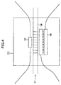
- Fig. 4 showing a block diagram of the wavelength gain characteristic shift slope filter.
- the wavelength gain characteristic shift slope filter 111 includes the optical filter 138 having a temperature dependency, a Peltier element 139 as a temperature adjuster, and a thermistor resistance 140 for detecting the temperature of the optical filter 138.
- an etalon filter or a fiber Bragg grating type filter can be used as the optical filter 138.
- any type of filter may be employed so long as it does not depart from the gist of the present invention.
- a fiber Bragg grating type filter called "long period grating" is employed as a device having a high temperature dependency.
- Fig. 5 shows wavelength-gain curves of an EDF found with an input level as a parameter
- Fig. 6 is a curve obtained continuously arranging the four wavelength-gain curves of Fig. 5
- Fig. 7 is a curve corresponding to an upside-down version of Fig. 6, which is the filter characteristic curve.
- Fig. 5 is a curve plotting input levels as parameters, showing a relationship between the wavelength and gain of the EDF in the ⁇ 2 band.
- the curve having a gain 36dB at 1532.5nm has a lowest input level
- the curve having a gain of 26dB at 1532.5nm has a highest input level.
- Fig. 6 is an approximation curve depicted by shifting the four wavelength-gain curves of Fig. 5 little by little in their wavelength axis direction while maintaining their shapes and by approximating all points to the approximation curve. This means that the curve of Fig. 6 is reproduced by continuously shifting the curves showing variations in the gain characteristic generated in the same ⁇ 2 wavelength band in the wavelength axis direction.
- Fig. 7 is a graph showing an insertion loss characteristic of the optical filter 138 and inversed to that of Fig. 6.
- the filter is able to be designed with an accuracy of 0.1dB.
- the ⁇ 2 wavelength band is originally 3nm, but the optical filter 138 has a band of 7nm and a loss characteristic corresponding to all the input levels shown in Fig. 5.
- the fiber Bragg grating type filter of the present embodiment has a temperature characteristic of 0.08nm/°C and can shift its wavelength by 4nm by providing a temperature change of about 50°C by means of the Peltier element. More specifically, when the variable temperature zone has a center temperature of 25°C, the center of the 7nm band of the optical filter 138 is made to coincide with the central wavelength of the ⁇ 2 band at 25°C. As a result, the loss characteristic of the optical filter can be varied by -2nm by shifting the temperature by 25°C toward its lower temperature side and by +2nm by shifting the temperature by 25°C toward its higher temperature side.
- the function of the wavelength gain characteristic shift slope filter 111 will be explained.
- the optical amplifier providing a constant output level provides a large gain to the optical signal, which results in that a gain deviation depending on wavelengths becomes large as shown by the uppermost curve in Fig. 5.
- the Peltier element 139 in Fig. 4 acts to increase the temperature, thereby increasing the temperature of the optical filter 138.
- the temperature increase causes filter characteristic of the optical filter 138 to be shifted to the higher wavelength side in Fig. 7, thereby enabling compensation for the inter-wavelength deviation of the gain.
- the temperature characteristic of the filter has been set at 0.08nm/°C in the present embodiment, the temperature change range can be made narrow by employing a device having a large temperature dependency.
- the filter temperature characteristic is set at 0.01nm/°C or more, since a shift of 0.5nm ca be obtained in a temperature range of 0-50°C, the effect of the present invention can be sufficiently obtained in some wavelength band.
- nm/°C is merely a representation means for approximating a characteristic for easy understanding and expression and thus the characteristic may be of a negative or vary with the temperature zone.
- a device can be employed that the characteristic is set at +0.01nm/°C, -0.01nm/°C, 0.03nm/°C in a range of 0-20°C, or 0.09nm/°C in a range of 20-50°C.
- the boundary between the wavelength bands for the optical signals is set to such a wavelength as to give an inflection point to the wavelength-gain characteristic of the EDF of the optical amplifier.
- the filter characteristic can be controlled in a narrow variable temperature range.
- wavelength gain characteristic shift slope filters as mentioned above in cascade.
- a more complex wavelength characteristic can be realized.
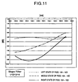
- Figs. 10A to 10D and 11 show three temperature types of wavelength transmission characteristics in four types of filters, respectively.
- Fig. 11 is a diagram for explaining a wavelength transmission characteristic of the four types of filters of Fig. 10A to 10D connected in cascade.
- Figs. 10A to 10D their ordinate denotes insertion loss (dB) and abscissa denotes wavelength (nm).
- the diagrams horizontally arranged in respective four types of filters not necessarily correspond to the same temperature sets.
- the present embodiment is the same in shifting the slope of the wavelength transmission characteristic as in the foregoing embodiment, but different therefrom in that the temperatures of the four filters are independently varied to change their characteristics and these characteristics are overlapped in cascade.
- the filters 1, 2, 3 and 4 are all independently varied, as will be clear from Figs. 10A to 10D.
- Fig. 11 shows a characteristic corresponding to an combination of the slope characteristics of the four filters of Figs. 10A to 10D connected in cascade. That is, Fig. 11 shows slope characteristics obtained when the three states of each of the four filters of Figs. 10A to 10D are overlapped. It will be clearly appreciated from Fig. 11 that the slope characteristic can be effectively made varied.
- the slope characteristic of the filter can be made varied more easily and effectively. It is desirable that the slope characteristics of the filters be designed independently so that the overlapped slope characteristic can have a desired slope.
- optical amplifiers of the present embodiment are intended to perform such control operation that an optical output level of the optical amplifier for each signal to be eventually output to the line becomes constant independently of the input level to the optical amplifier.
- the dispersion compensator has such an input power restriction that introduction of light at a level of a predetermined value or more causes observation of a signal waveform distortion phenomenon due to the nonlinear effect of the light.
- the signal input level of the dispersion compensator is controlled to be +0dBm or less for each signal.
- the first optical amplifier 64 can find an amplification gain by monitoring its input and output levels, and the gain is controllably adjusted by the first controller 66 according to the input level. For example, when the input level is a lowest level of -30dBm, the gain is controlled to be about 30dB. When the input level is +5dBm, its gain is controlled to be about 5dB.
- the optical gain adjusters 105, 106, 107 and 108 monitor their optical output levels and control their output to be as constant as +0dBm or less for each signal wavelength.
- the gains of the optical gain adjusters 105, 106, 107 and 108 are determined to have predetermined values.
- the determined amplified or attenuated gains can be monitored on input monitors to the optical gain adjusters 105, 106, 107 and 108.
- the optical signal passed through this path is passed through the dispersion compensator 85 and then amplified by the second optical amplifier 87.
- the second optical amplifier 87 controls its output such that its line light output level becomes as constant as +8dBm per each signal wavelength.
- the gain of the second optical amplifier 87 is determined by the loss of the dispersion compensator 85. The determined amplified gain can be monitored on an input monitor to the second optical amplifier 87.
- the gain from the input of the optical amplifier to the output thereof is determined for each path, and these gain information are collected at wavelength gain characteristic shift slope filter controllers 133, 134, 135 and 136.
- the optical gain adjusters 105, 106, 107 and 108 have a gain of 10dB
- the second optical amplifier 87 has a gain of 18dB; then these gain information are collected at the wavelength gain characteristic shift slope filter controllers 133, 134, 135 and 136.
- the gain deviation varies depending on the gain of the optical amplifier.
- Adjustments of the wavelength gain characteristic shift slope filters 109, 110, 111 and 112 to the respective gains are previously set; and the wavelength gain characteristic shift slope filters 109, 110, 111 and 112 are controlled by the wavelength gain characteristic shift slope filter controllers 133, 134, 135 and 136 to perform predetermined adjusting operation based on the detected gain information.
- Wavelength multiplexed outputs of the optical amplifiers are supplied into optical demultiplexers 137-1 and 137-2 to be demultiplexed for each wavelength.
- the demultiplexed wavelengths are split respectively by optical splitters 138-1 to 138-n and monitored by light receivers 139-1 to 139-n for the respective wavelengths.
- the wavelength gain characteristic shift slope filters 109, 110, 111 and 112 are controlled so that the optical levels of the respective wavelengths become predetermined values.
- Such an arrangement enables direct monitoring of the wavelength characteristics, thus increasing its control accuracy. Further, since the optical power auxiliary adjuster can be controlled not depending on the gains of the optical amplifiers within the optical amplification device, the optical transmission equipment can be increased in its control flexibility when actually used.
- Optical gain adjusters 140-1 to 140-n and optical demultiplexers 137-1 and 137-2 have each such a structure as to utilize an optical power adjuster 8 which adjusts the respective signal wavelengths independently, and are arranged so that light receivers 143-1 to 143-n controllably monitor light split by optical splitters 141-2 to 142-n, thus obtaining a constant output level.
- optical power adjuster 8 and fourth optical gain controller 94 may be located downstream of the optical demultiplexer 90 or 101.
- Fig. 9 is a block diagram of optical transmission equipment in accordance with an embodiment of the present invention.
- a method for controlling respective optical amplifiers and optical gain adjusters is substantially the same as that in Figs. 1 and 8.
- Optical gain adjusters 146-1 to 146-n and optical multiplexers 150-1 and 150-2 correspond each to an application of the optical power adjuster 8 which adjusts the respective signal wavelengths independently.
- Controllers 147-1 to 147-n are arranged so that light receivers 145-1 to 145-n detect the input light by monitoring light split by optical splitters 144-1 to 144-n and light receivers 149-1 to 149-n monitor light split by optical splitters 148-1 to 148-n, thereby controlling the controllerls 147-1 to 147-n and obtaining constant output levels.
- the respective signal outputs are sent to the optical multiplexers 150-1 and 150-2 for their multiplexing.
- the wavelength gain characteristic shift slope filters 109, 110, 111 and 112 are controlled so that the output light levels of the respective wavelengths are monitored and amplified with predetermined gain values.
- optical power adjuster 8 and fourth optical gain controller 94 may be located upstream of the optical splitter 90 or 101.
- Such an arrangement enables direct control of an amplification gain for an input signal gain, thus improving its control accuracy. Since the wavelength gain characteristic shift slope filter can be controlled not depending on the gains of optical amplifiers within the optical amplification device, the optical transmission equipment can increase its control flexibility when actually used.
- the gain characteristic of the rare-earth-element-doped optical fiber as the optical amplifying medium is regarded as a curve having a plurality of inflection points and wavelength division is carried out substantially in the vicinity of the inflection points.
- Each divided wavelength band is located between the inflection points.
- an optical filter possessed by the optical power auxiliary adjuster of the present invention is featured in that the filter has a large temperature characteristic.
- the function realizable by the present invention is to make gain characteristics of originally different wavelength bands appear in desired wavelength bands to obtain a desired gain characteristic by changing the temperature.
- a narrow required temperature variable width is valid from the control viewpoint.
- an optical filter having a large temperature dependency is necessary.
- This system of realizing it merely by shifting the gain characteristics present across the originally-different wavelength bands can have a simple arrangement and can be controlled functionally easily with an improved reliability.
- the temperature control method has been employed as the method for making the gain characteristics of the originally-different wavelength bands appear in the desired wavelength bands to obtain a desired gain characteristic in the present embodiment
- the present invention is not necessarily limited to this arrangement.
- a method for changing the wavelength characteristics spectrally to obtain a desired gain characteristic may be employed.
- the optical gain adjuster can adjust a light power of a band and a gain deviation in the band simultaneously.
- a compensation for the gain deviation may become lack.
- the wavelength gain characteristic shift slope filter can adjust the gain deviation but at the same time can cause a change of a loss in the band, thus changing the light power in the band.
- the optical gain adjuster and wavelength gain characteristic shift slope filter are provided separately at the same time, the effects of the adjuster and filter can be mutually complemented, thus leading to an additional improvement over the effect of the prior art.
- the gain deviations caused by the optical amplifiers within the optical amplification device can be effectively adjusted. Further, gain deviations accumulated from an optical amplification device at a preceding stage, which results in a problem when the optical amplification devices are connected in multiple stages, can be sufficiently corrected and adjusted (the gain deviations will not be accumulated even when the gain deviations take place in the preceding-stage optical amplification device), whereby the transmission system can be largely improved.
- the wavelength gain characteristic shift slope filter is not limited to the illustrated position but may be installed, for example, at the preceding or subsequent stage of the optical gain adjuster.
- the wavelength gain characteristic shift slope filter for dynamically equalizing its gain according to its input level can be implemented. Further, there can be provided optical transmission equipment which can effectively utilize wavelength bands suitable for wavelength division multiplexing. Furthermore, there can be provided an optical transmission method suitable for wavelength division multiplexing.
Landscapes
- Engineering & Computer Science (AREA)
- Computer Networks & Wireless Communication (AREA)
- Signal Processing (AREA)
- Physics & Mathematics (AREA)
- Electromagnetism (AREA)
- Spectroscopy & Molecular Physics (AREA)
- Lasers (AREA)
- Optical Communication System (AREA)
Abstract
Description
Claims (6)
- A wavelength gain characteristic shift slope filter comprising:an optical filter (138) for obtaining slope characteristics corresponding to wavelength gain characteristics with respect to a plurality of input levels of an optical amplifier by changing a temperature thereof; anda Peltier element (139) for controlling a temperature of the optical filter.
- An optical transmission equipment comprising:a wavelength gain characteristic shift slope filter (109, 110, 111, 112) for compensating for wavelength gain characteristic according to input level;an optical gain adjuster (105, 106, 107, 108); andan optical amplifier (98, 87) for amplifying a optical signal having a plurality of wavelengths.
- An optical transmission equipment comprising:an wavelength gain characteristic shift slope filter (109, 110, 111, 112) including an optical filter (138) for obtaining slope characteristics corresponding to wavelength gain characteristics with respect to a plurality of input levels of an optical amplifier by changing a temperature thereof and also including a Peltier element (139) for controlling the temperature of the optical filter (138);an optical gain adjuster (105, 106, 107, 108) including a first impurity-doped fiber (301) and a first exciting light source (302); andan optical amplifier (98, 87) including a second impurity-doped fiber and a second exciting light source for amplifying a optical signal having a plurality of wavelengths.
- An optical transmission equipment wherein an amplification band is divided at least with wavelengths providing inflection points to a wavelength gain characteristic of an impurity-doped fiber and gain adjustment is carried out for each of the divided wavelength bands.
- An optical transmission equipment comprising:a plurality of wavelength gain characteristic shift slope filters (109, 110, 111, 112) connected in cascade for compensating for wavelength gain characteristics associated with input levels;an optical gain adjuster (105, 106, 107, 108); andan optical amplifier (98, 87) for amplifying a optical signal having a plurality of wavelengths.
- A method of optical signal transmission, said method comprising the steps of:dividing an amplification band with wavelengths at inflection points in a wavelength gain characteristic of an impurity-doped fiber; andperforming gain adjustment for each of the divided wavelength bands.
Applications Claiming Priority (2)
| Application Number | Priority Date | Filing Date | Title |
|---|---|---|---|
| JP19123099 | 1999-07-06 | ||
| JP19123099A JP4340355B2 (en) | 1999-07-06 | 1999-07-06 | Wavelength gain characteristic shift filter, optical transmission apparatus and optical transmission method |
Publications (2)
| Publication Number | Publication Date |
|---|---|
| EP1067725A2 true EP1067725A2 (en) | 2001-01-10 |
| EP1067725A3 EP1067725A3 (en) | 2005-08-31 |
Family
ID=16271074
Family Applications (1)
| Application Number | Title | Priority Date | Filing Date |
|---|---|---|---|
| EP00114314A Withdrawn EP1067725A3 (en) | 1999-07-06 | 2000-07-04 | Filter with variable transmission characteristic |
Country Status (3)
| Country | Link |
|---|---|
| US (2) | US6580550B1 (en) |
| EP (1) | EP1067725A3 (en) |
| JP (1) | JP4340355B2 (en) |
Cited By (1)
| Publication number | Priority date | Publication date | Assignee | Title |
|---|---|---|---|---|
| US6768579B2 (en) * | 2000-08-18 | 2004-07-27 | Siemens Aktiengesellschaft | Optical amplifier arrangement having a variably settable attenuator |
Families Citing this family (11)
| Publication number | Priority date | Publication date | Assignee | Title |
|---|---|---|---|---|
| JP4340355B2 (en) * | 1999-07-06 | 2009-10-07 | 株式会社日立コミュニケーションテクノロジー | Wavelength gain characteristic shift filter, optical transmission apparatus and optical transmission method |
| JP2002158636A (en) * | 2000-03-29 | 2002-05-31 | Hitachi Ltd | Optical transmission device and its monitoring system |
| US6751012B1 (en) * | 2000-12-14 | 2004-06-15 | Tyco Telecommunications (Us) Inc. | Method and apparatus for measuring noise figure in optical amplifiers |
| US7106969B1 (en) * | 2001-02-12 | 2006-09-12 | Atrica Israel Ltd. | Optical network terminator |
| US7031613B1 (en) * | 2001-07-17 | 2006-04-18 | Cisco Technology, Inc. | Chromatic dispersion compensation by sub-band |
| US7085496B2 (en) * | 2002-05-30 | 2006-08-01 | Fujitsu Limited | Passive add/drop amplifier for optical networks and method |
| US7075712B2 (en) * | 2002-05-30 | 2006-07-11 | Fujitsu Limited | Combining and distributing amplifiers for optical network and method |
| JP4246644B2 (en) * | 2004-01-21 | 2009-04-02 | 富士通株式会社 | Optical receiver and optical transmission device |
| JP4725951B2 (en) * | 2004-07-28 | 2011-07-13 | 富士通株式会社 | Wavelength multiplexed signal light amplification method and optical amplifier |
| RU2402050C1 (en) * | 2009-06-04 | 2010-10-20 | Учреждение Российской академии наук ИНСТИТУТ ФИЗИКИ ТВЕРДОГО ТЕЛА РАН (ИФТТ РАН) | Neutral light filter |
| US20190324212A1 (en) * | 2017-01-06 | 2019-10-24 | Molex, Llc | Optical arrangement for suppressing outerband crosstalk in a wavelength selective switch |
Family Cites Families (30)
| Publication number | Priority date | Publication date | Assignee | Title |
|---|---|---|---|---|
| US628361A (en) * | 1899-04-22 | 1899-07-04 | John Peirce Shank | Lady's sewing-cabinet. |
| US5579143A (en) * | 1993-06-04 | 1996-11-26 | Ciena Corporation | Optical system with tunable in-fiber gratings |
| US5541766A (en) * | 1994-11-30 | 1996-07-30 | At&T Corp. | Gain control for optically amplified systems |
| JPH08237203A (en) * | 1995-02-23 | 1996-09-13 | Fujitsu Ltd | Optical filter array, optical transmitter and optical transmission system |
| FR2731082B1 (en) * | 1995-02-28 | 1997-04-04 | France Telecom | OPTICAL INSERTION-EXTRACTION MULTIPLEXER USING OPTICAL CIRCULATORS AND PHOTO-WRITTEN BRAGG ARRAYS |
| JPH08278523A (en) * | 1995-04-05 | 1996-10-22 | Hitachi Ltd | Optical amplifier |
| JPH0918416A (en) * | 1995-06-28 | 1997-01-17 | Hitachi Ltd | Optical amplifier |
| EP0784364A4 (en) * | 1995-07-05 | 2000-02-23 | Hitachi Ltd | METHOD FOR CONTROLLING A LIGHT AMPLIFIER DEVICE, LIGHT AMPLIFIER, AND SYSTEM USING THE SAME |
| US6111681A (en) * | 1996-02-23 | 2000-08-29 | Ciena Corporation | WDM optical communication systems with wavelength-stabilized optical selectors |
| JP3556379B2 (en) * | 1996-03-07 | 2004-08-18 | 富士通株式会社 | Optical transmission system |
| IT1283224B1 (en) * | 1996-03-11 | 1998-04-16 | Pirelli Cavi Spa | APPARATUS AND METHOD OF PROTECTION FOR OPTICAL FIBER DEVICES |
| FR2747527B1 (en) * | 1996-04-12 | 1998-05-15 | Cit Alcatel | METHOD AND DEVICE FOR AMPLIFYING CHANNELS EXTRACTED FROM A WAVELENGTH MULTIPLEX |
| JPH10145298A (en) * | 1996-11-08 | 1998-05-29 | Kokusai Denshin Denwa Co Ltd <Kdd> | Optical demultiplexer for WDM communication |
| US5900969A (en) * | 1997-02-14 | 1999-05-04 | Lucent Technologies Inc. | Broadband flat gain optical amplifier |
| CA2228122A1 (en) * | 1997-02-17 | 1998-08-17 | Kevin W. Bennett | Pump wavelength tuning of optical amplifiers and use of same in wavelength division multiplexed systems |
| US6049417A (en) * | 1997-06-02 | 2000-04-11 | Lucent Technologies Inc. | Wide band optical amplifier |
| US6151157A (en) * | 1997-06-30 | 2000-11-21 | Uniphase Telecommunications Products, Inc. | Dynamic optical amplifier |
| AU8175098A (en) * | 1997-06-30 | 1999-01-19 | Uniphase Telecommunications Products, Inc. | Method and apparatus for dynamically equalizing gain in an optical network |
| JP3771010B2 (en) * | 1997-08-06 | 2006-04-26 | 富士通株式会社 | Method for optical amplification and system for implementing the method |
| US5987200A (en) | 1997-10-27 | 1999-11-16 | Lucent Technologies Inc. | Device for tuning wavelength response of an optical fiber grating |
| JP3884841B2 (en) * | 1997-11-14 | 2007-02-21 | 株式会社日立コミュニケーションテクノロジー | Optical transmission system and optical communication device |
| JP3453301B2 (en) * | 1998-04-27 | 2003-10-06 | 富士通株式会社 | Active optical fiber and optical fiber amplifier |
| US6275629B1 (en) * | 1998-09-11 | 2001-08-14 | Lucent Technologies Inc. | Optical grating devices with adjustable chirp |
| JP2000106544A (en) * | 1998-09-28 | 2000-04-11 | Fujitsu Ltd | Optical amplifier and WDM optical transmission system |
| JP2000180803A (en) * | 1998-12-15 | 2000-06-30 | Sumitomo Electric Ind Ltd | Multi-channel optical variable attenuator |
| JP2000299518A (en) * | 1999-02-10 | 2000-10-24 | Oki Electric Ind Co Ltd | Optical fiber amplifier and control thereof |
| JP2000277842A (en) * | 1999-03-23 | 2000-10-06 | Oki Electric Ind Co Ltd | Optical components, and optical amplifier and characteristics control method for the same |
| JP4340355B2 (en) * | 1999-07-06 | 2009-10-07 | 株式会社日立コミュニケーションテクノロジー | Wavelength gain characteristic shift filter, optical transmission apparatus and optical transmission method |
| CA2314420C (en) * | 1999-07-27 | 2008-06-03 | Sumitomo Electric Industries, Ltd. | Optical filter |
| US6307668B1 (en) * | 1999-10-04 | 2001-10-23 | Optigain, Inc. | Ultra-wide bandwidth fiber based optical amplifier |
-
1999
- 1999-07-06 JP JP19123099A patent/JP4340355B2/en not_active Expired - Fee Related
-
2000
- 2000-07-04 EP EP00114314A patent/EP1067725A3/en not_active Withdrawn
- 2000-07-05 US US09/609,595 patent/US6580550B1/en not_active Expired - Fee Related
-
2003
- 2003-04-23 US US10/421,567 patent/US6867909B2/en not_active Expired - Fee Related
Cited By (1)
| Publication number | Priority date | Publication date | Assignee | Title |
|---|---|---|---|---|
| US6768579B2 (en) * | 2000-08-18 | 2004-07-27 | Siemens Aktiengesellschaft | Optical amplifier arrangement having a variably settable attenuator |
Also Published As
| Publication number | Publication date |
|---|---|
| US20030193714A1 (en) | 2003-10-16 |
| EP1067725A3 (en) | 2005-08-31 |
| JP2001024262A (en) | 2001-01-26 |
| US6867909B2 (en) | 2005-03-15 |
| US6580550B1 (en) | 2003-06-17 |
| JP4340355B2 (en) | 2009-10-07 |
Similar Documents
| Publication | Publication Date | Title |
|---|---|---|
| US6636659B2 (en) | Optical amplification apparatus and optical transmission system | |
| US6724526B1 (en) | Inter-wavelength light power deviation monitoring method and optical equalizer and optical amplifier utilizing the method | |
| JP4498509B2 (en) | Control device and control method of wavelength division multiplexing optical amplifier | |
| US7119950B2 (en) | Amplification method and optical amplifier for wavelength division multiplexed signal light | |
| US6400498B1 (en) | Optical signal repeating and amplifying device and optical level adjusting device | |
| EP1067725A2 (en) | Filter with variable transmission characteristic | |
| KR100715642B1 (en) | Optical amplifier and optical amplification method | |
| US6606189B2 (en) | Light amplifier and light amplifying method | |
| US6456428B1 (en) | Optical amplifier | |
| EP1788730B1 (en) | Optical amplification unit with span loss tilt compensation | |
| US8189256B2 (en) | Gain equalizer, optical amplifier, loss compensation method, and optical amplification method | |
| JP4234382B2 (en) | Optical amplification method, apparatus thereof, and optical amplification repeater system using the apparatus | |
| US20070058241A1 (en) | Optical amplification apparatus having function of flattening channel output spectrum | |
| US6646792B2 (en) | Light amplifier and light transmission system using the same | |
| US7391560B2 (en) | Multistage optical amplifier having tilt compensation feature | |
| JPH10322313A (en) | Wavelength multiplexing transmitter | |
| EP0959577A2 (en) | Optical signal repeating and amplifying device and optical level adjusting device | |
| JP2000004061A (en) | Optical gain equalizer | |
| US20030095738A1 (en) | Planar optical circuit and optical transmission system | |
| JP3609968B2 (en) | Optical amplifier | |
| US20110311236A1 (en) | Optical amplifier, control method therefor, and optical transmission system | |
| EP0926849A2 (en) | Optical amplifier for wavelength division multiplexing transmission | |
| JP2004296581A (en) | Optical amplifier and control method therefor | |
| JPH11220196A (en) | Optical amplifier | |
| EP0930677A2 (en) | Direct optical amplifier |
Legal Events
| Date | Code | Title | Description |
|---|---|---|---|
| PUAI | Public reference made under article 153(3) epc to a published international application that has entered the european phase |
Free format text: ORIGINAL CODE: 0009012 |
|
| AK | Designated contracting states |
Kind code of ref document: A2 Designated state(s): AT BE CH CY DE DK ES FI FR GB GR IE IT LI LU MC NL PT SE |
|
| AX | Request for extension of the european patent |
Free format text: AL;LT;LV;MK;RO;SI |
|
| PUAL | Search report despatched |
Free format text: ORIGINAL CODE: 0009013 |
|
| AK | Designated contracting states |
Kind code of ref document: A3 Designated state(s): AT BE CH CY DE DK ES FI FR GB GR IE IT LI LU MC NL PT SE |
|
| AX | Request for extension of the european patent |
Extension state: AL LT LV MK RO SI |
|
| 17P | Request for examination filed |
Effective date: 20050921 |
|
| AKX | Designation fees paid |
Designated state(s): DE FR GB |
|
| 17Q | First examination report despatched |
Effective date: 20071009 |
|
| GRAP | Despatch of communication of intention to grant a patent |
Free format text: ORIGINAL CODE: EPIDOSNIGR1 |
|
| RIC1 | Information provided on ipc code assigned before grant |
Ipc: H04J 14/02 20060101AFI20130315BHEP Ipc: H04B 10/294 20130101ALI20130315BHEP Ipc: H04B 10/2507 20130101ALI20130315BHEP |
|
| INTG | Intention to grant announced |
Effective date: 20130409 |
|
| STAA | Information on the status of an ep patent application or granted ep patent |
Free format text: STATUS: THE APPLICATION IS DEEMED TO BE WITHDRAWN |
|
| 18D | Application deemed to be withdrawn |
Effective date: 20130820 |