EP1067696A2 - Distortion compensation method and wireless communication apparatus - Google Patents
Distortion compensation method and wireless communication apparatus Download PDFInfo
- Publication number
- EP1067696A2 EP1067696A2 EP00305641A EP00305641A EP1067696A2 EP 1067696 A2 EP1067696 A2 EP 1067696A2 EP 00305641 A EP00305641 A EP 00305641A EP 00305641 A EP00305641 A EP 00305641A EP 1067696 A2 EP1067696 A2 EP 1067696A2
- Authority
- EP
- European Patent Office
- Prior art keywords
- signal
- power amplification
- input
- high frequency
- power amplifier
- Prior art date
- Legal status (The legal status is an assumption and is not a legal conclusion. Google has not performed a legal analysis and makes no representation as to the accuracy of the status listed.)
- Withdrawn
Links
Images



Classifications
-
- H—ELECTRICITY
- H03—ELECTRONIC CIRCUITRY
- H03F—AMPLIFIERS
- H03F1/00—Details of amplifiers with only discharge tubes, only semiconductor devices or only unspecified devices as amplifying elements
- H03F1/32—Modifications of amplifiers to reduce non-linear distortion
- H03F1/3241—Modifications of amplifiers to reduce non-linear distortion using predistortion circuits
- H03F1/3247—Modifications of amplifiers to reduce non-linear distortion using predistortion circuits using feedback acting on predistortion circuits
-
- H—ELECTRICITY
- H03—ELECTRONIC CIRCUITRY
- H03F—AMPLIFIERS
- H03F1/00—Details of amplifiers with only discharge tubes, only semiconductor devices or only unspecified devices as amplifying elements
- H03F1/02—Modifications of amplifiers to raise the efficiency, e.g. gliding Class A stages, use of an auxiliary oscillation
- H03F1/0205—Modifications of amplifiers to raise the efficiency, e.g. gliding Class A stages, use of an auxiliary oscillation in transistor amplifiers
- H03F1/0261—Modifications of amplifiers to raise the efficiency, e.g. gliding Class A stages, use of an auxiliary oscillation in transistor amplifiers with control of the polarisation voltage or current, e.g. gliding Class A
-
- H—ELECTRICITY
- H04—ELECTRIC COMMUNICATION TECHNIQUE
- H04B—TRANSMISSION
- H04B1/00—Details of transmission systems, not covered by a single one of groups H04B3/00 - H04B13/00; Details of transmission systems not characterised by the medium used for transmission
- H04B1/02—Transmitters
- H04B1/04—Circuits
-
- H—ELECTRICITY
- H03—ELECTRONIC CIRCUITRY
- H03F—AMPLIFIERS
- H03F2200/00—Indexing scheme relating to amplifiers
- H03F2200/451—Indexing scheme relating to amplifiers the amplifier being a radio frequency amplifier
Definitions
- This invention relates to a method of compensating for a nonlinear distortion of a power amplifier of a transmission section of a wireless communication apparatus, and a wireless communication apparatus which compensates for a nonlinear distortion of a power amplifier of a transmission section.
- the demand for linearity of a power amplifier for transmission becomes severe as increase of the speed and capacity of communication proceeds.
- the power efficiency of the power amplifier decreases, and this prevents, for example, elongation of the time within which a terminal telephone set of a digital portable telephone system can enjoy a continuous service. Therefore, it has been proposed to compensate for a nonlinear distortion of a power amplifier to augment the power efficiency of the power amplifier.
- FIG. 14 illustrates a distortion compensation method disclosed in Japanese Patent No. 2,689,011, "Linear Transmission Apparatus”.
- an input signal Si of a modulated wave from an input terminal 101 is inputted to a power amplifier 91 through a directional coupler 92 and a power control circuit 93.
- An output signal of the power amplifier 91 is led out as an output signal So to an output terminal 102 through another directional coupler 94.
- the input signal Si is branched by the directional coupler 92 and supplied to an envelope detection circuit 95, by which an envelope of the input signal Si is detected.
- the envelope detection signal of the envelope detection circuit 95 is supplied to a dc voltage conversion circuit 96, by which a dc voltage from a power supply terminal 103 is converted in accordance with the envelope of the input signal Si.
- a dc voltage after the conversion of the dc voltage conversion circuit 96 is supplied as a power supply voltage to the power amplifier 91.
- the output signal So is branched by the directional coupler 94 and supplied to another envelope detection circuit 97, by which an envelope of the output signal So is detected.
- the envelope detection signal of the envelope detection circuit 97 is supplied together with the envelope detection signal from the envelope detection circuit 95 to a difference signal production circuit 98.
- the difference signal production circuit 98 produces a signal of a difference between the envelope of the input signal Si and the envelope of the output signal So.
- the difference signal of the difference signal production Circuit 98 is supplied through a dc amplifier 99 to the power control circuit 93.
- the power control circuit 93 controls the input power of the power amplifier 91 in accordance with the difference between the envelope of the input signal Si and the envelope of the output signal So.
- the power supply voltage of the power amplifier 91 is controlled in accordance with the envelope of the input signal Si to decrease a nonlinear distortion of the input signal Si, and the input power of the power amplifier 91 is controlled in accordance with the difference between the envelope of the input signal Si and the envelope of the output signal So to absorb a gain variation of the power amplifier 91 which is caused by a temperature variation or the like.
- a distortion compensation method for compensating for a nonlinear distortion of a power amplifier comprising a detection step of detecting envelopes of an input signal and an output signal of the power amplifier individually, and an addition step of adding a signal corresponding to a finite difference between the detection signals of the envelopes obtained by the detection step to the input signal of the power amplifier.
- the distortion compensation method not a signal obtained by modulating a power supply voltage of the power amplifier and amplifying the modulated power supply voltage by the power amplifier is amplitude modulated, but a signal for compensation is added to an input signal of the power amplifier. Consequently, a nonlinear distortion of the power amplifier can be reduced without production of a distortion by modulation. Besides, since a signal corresponding to a finite difference between an envelope of the input signal and an envelope of an output signal of the power amplifier is added as the signal for compensation, also a nonlinear distortion which cannot be detected from the envelope of the input signal and does not rely upon the power supply voltage of the power amplifier can be reduced with certainty.
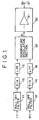
- FIG. 1 shows an example of a wireless communication apparatus of the present invention. More particularly, FIG. 1 shows an example of a wireless communication apparatus wherein a nonlinear distortion of a power amplifier of a transmission section is compensated for by a distortion compensation method of the present invention.
- the wireless communication apparatus shown in FIG. 1 is formed as a terminal telephone set of a digital portable telephone system.
- digital quadrature baseband signals I and Q are supplied through roll off filters 11 and 12 to D/A converters 13 and 14, respectively, by which they are converted into analog signals.
- the analog quadrature baseband signals obtained by the D/A converters 13 and 14 are supplied through low-pass filters 15 and 16 to a quadrature modulation section 20, respectively. Consequently, a quadrature modulated high frequency signal Si is obtained by the quadrature modulation section 20.
- the high frequency signal Si is amplified by a high frequency power amplifier 31 of a high frequency power amplification section 30 so that a transmission high frequency signal So is obtained at an output terminal 37. Further, a nonlinear distortion of the high frequency power amplifier 31 is compensated for in the following manner by the high frequency power amplification section 30.
- the high frequency power amplifier 31 is referred to simply as power amplifier 31.
- FIG. 2 shows a form of the high frequency power amplification section 30.
- the input high frequency signal Si from the quadrature modulation section 20 of FIG. 1 is supplied to an input terminal 32 and branched to input high frequency signals S1 and S5 by a directional coupler 33.
- the input high frequency signal S1 is inputted to a gain control circuit 34.
- An addition circuit 35 on the output side of the gain control circuit 34 adds a finite difference signal Sa from a comparator 44 which is hereinafter described to a high frequency signal S2 from the gain control circuit 34.
- a high frequency signal S3 from the addition circuit 35 is amplified by the power amplifier 31.
- a high frequency signal S4 of an output of the power amplifier 31 is branched to two output high frequency signals So and S6 by a directional coupler 36.
- the output high frequency signal So is extracted as a transmission high frequency signal to the output terminal 37.
- the other input high frequency signal S5 branched by the directional coupler 33 is supplied to an envelope detection circuit 41, by which an envelope of the high frequency signal S5 is detected. Then, an envelope detection signal D5 of the envelope detection circuit 41 is supplied to one of a pair of input terminals of the comparator 44. Meanwhile, the level of the other output high frequency signal S6 branched by the directional coupler 36 is adjusted in such a manner as hereinafter described by a level adjustment circuit 42. Then, a high frequency signal S7 after the adjustment by the level adjustment circuit 42 is supplied to another envelope detection circuit 43, by which an envelope of the high frequency signal S7 is detected. Then, an envelope detection signal D7 of the envelope detection circuit 43 is supplied to the other input terminal of the comparator 44.
- a signal Sa of a finite difference between the input envelope detection signal D5 and the output envelope detection signal D7 is obtained from the comparator 44.
- the finite difference signal Sa is added to the high frequency signal S2 from the gain control circuit 34 by the addition circuit 35.
- the finite difference signal Sa is supplied to a low-pass filter 45, from which a component of a low frequency in the finite difference signal Sa is extracted. Then, a signal S8 from the low-pass filter 45 is added to a gain control signal VGO from a control section 50 by an addition circuit 46, and the level of a signal S9 from the addition circuit 46 is adjusted by a level adjustment circuit 47. Then, the gain of the gain control circuit 34 is controlled in the following manner with a gain control signal VGC after the adjustment of the level adjustment circuit 47.
- the gain thereof is kept fixed irrespective of variation of an environmental parameter such as the temperature or the power supply voltage.
- the input high frequency signals Si, S1 and S5 and the input envelope detection signal D5 are signals free from distortion.
- the output high frequency signals So, S6 and S7 and the output envelope detection signal D7 are signals which have only a nonlinear distortion of the power amplifier 31 if such environmental parameters as the temperature and the power supply voltage do not vary.
- the output high frequency signals So, S6 and S7 and the output envelope detection signal D7 become signals which include, in addition to a distortion component, an offset component of a level which originates from the gain variation of the power amplifier 31.
- the level adjustment circuit 42 is set so that the input envelope detection signal D5 and the output envelope detection signal D7 may have an equal level under certain environmental parameters.
- the finite difference signal Sa from the comparator 44 includes only a component included in the output envelope detection signal D7 if environmental parameters do not vary, but if an environmental parameter varies, then the finite difference signal Sa becomes a sum of the distortion component mentioned and the offset component described above.
- the component of the finite difference signal Sa which has a low frequency that is, the offset component described above originating from a variation of an environmental parameter
- a component of the finite difference signal Sa which has a high frequency that is, an envelope variation component of the distortion component, is cut off.
- the signal S8 is zero.
- the gain of the gain control circuit 34 is controlled with the gain control signal VGC obtained by adding the signal S8 from the low-pass filter 45 to the gain control signal VGO from the control section 50 so that the signal S8 as the offset component originating from the variation of the environmental parameter may be zero.
- the gain of the high frequency power amplification section 30 is kept fixed.
- the gain of the power amplifier 31 is varied by variation of an environmental parameter, since the gain of the gain control circuit 34 varies by an equal amount in the opposite direction in response to the variation of the gain, the gain of the high frequency power amplification section 30 including the power amplifier 31 and the gain control circuit 34 is kept fixed. As a result, the variation of the gain of the power amplifier 31 is cancelled.
- the input voltage of the power amplifier 31 is represented by Vi
- the output voltage is represented by Vo
- the linear gain is represented by G (times). Since the power amplifier 31 has only a nonlinear distortion, amplitude suppression occurs in a high output power region.
- the signal Sa is added to the input high frequency signal S2 of the power amplifier 31, different from another case wherein a power supply voltage of a power amplifier is modulated to amplitude modulate a high frequency signal, distortion by modulation does not occur.
- the signal Sa of the finite difference between the input envelope detection signal D5 and the output envelope detection signal D7 is added as a signal for compensation, different from another case wherein a power supply voltage of a power amplifier is modulated in response to an input envelope detection signal, also a nonlinear distortion which cannot be detected from the input envelope detection signal D5 and does not rely upon the power supply voltage of the power amplifier 31, for example, a distortion which arises from a nonlinear parameter such as, for example, a parasitic capacitance Cgs between the gate and the source of a GaAs FET which forms the power amplifier 31, can be reduced with certainty.
- a nonlinear parameter such as, for example, a parasitic capacitance Cgs between the gate and the source of a GaAs FET which forms the power
- the addition circuit 35 includes, for example, as shown in FIG. 4, three resistors R1, R2 and R3 connected in a star connection. With the construction, since the addition circuit 35 is composed only of passive elements, pure addition is performed, and production of a distortion by modulation can be prevented with a higher degree of certainty.
- an adjacent channel leakage power ratio is -39 dBc.
- FIG. 7 a result of calculation of an output spectrum of the power amplifier 31 obtained by inputting the QPSK modulation signal to which the finite difference signal Sa is added by the addition circuit 35 as described above using the same power amplifier as the power amplifier 31 is illustrated in FIG. 7.
- the adjacent channel leakage power ratio is -88 dBc and exhibits augmentation by 49 dB when compared with that of another case wherein the distortion compensation of FIG. 6 is not performed.
- FIG. 8 shows an example of the gain control circuit 34 of FIG. 2 where it is formed as an attenuator which includes a FET.
- the source and the drain of a FET 61 are connected to a power supply line 62 of +3 V through resistors Rs and Rd. respectively.
- the gate of the FET 61 is connected through a resistor Rg to a terminal 63, to which the gain control signal VGC is supplied.
- the high frequency signal Si is inputted to a terminal 64 led out from the source of the FET 61, and the high frequency signal S2 is outputted from a terminal 65 led out from the drain of the FET 61.
- gain control circuit 34 where a GaAs JFET having a gate width of 1 mm is used as the FET 61, such an attenuation characteristic as illustrated in FIG. 9 is obtained, and by varying the gain control signal VGC within a range from 0 V to +3 V, gain control over approximately 10 dB is possible.
- FIG. 10 shows another example of the gain control circuit 34 of FIG. 2 wherein a dual-gate FET is used.
- the first gate G1 of a dual gate FET 71 is connected through a resistor Rb to a terminal 72 to which a bias voltage Vb is supplied.
- the drain D of the dual gate FET 71 is connected to a power supply through a load resistor Rr.
- the high frequency signal S1 is inputted to a terminal 73 led out from the first gate G1 of the dual gate FET 71, and the gain control signal VGC is supplied to another terminal 74 led out from the second gate G2 of the dual gate FET 71. Further, the high frequency signal S2 is outputted from a further terminal 75 led out from the drain D of the dual gate FET 71.
- the source S of the dual gate FET 71 is grounded.
- a GaAs JFET having a gate width of 200 ⁇ m is used as the dual gate FET 71 in the present gain control circuit 34, such a gain characteristic as illustrated in FIG. 11 is obtained, and by varying the gain control signal VGC within a range of 0 V to +2 V, gain control over approximate 15 dB is possible.
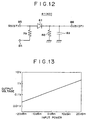
- FIG. 12 shows an example of the envelope detection circuits 41 and 43.
- a resistor 82 and a capacitor 83 are connected in parallel between the cathode of a diode 81 and the ground, and in order to augment the non-linearity of the diode 81 in a low signal region, the anode of the diode 81 is connected through a resistor Rb to a terminal 84 to which the bias voltage Vb is supplied.
- the high frequency signal S5 or S7 is inputted to a terminal 85 led out from the anode of the diode 81, and the envelope detection signal D5 or D7 is outputted from a terminal 86 led out from the cathode of the diode 81.
- the present envelop detection circuit 41 or 43 as a characteristic of an output voltage which is obtained as the envelope detection signal D5 or D7 with respect to an input power applied as the high frequency signal S5 or S7, such a characteristic as illustrated in FIG. 13 is obtained.
- the high frequency power amplification section of FIG. 2 is constructed such that the input high frequency signal Si obtained at the input terminal 32 is branched to two input high frequency signals S1 and S5 by the directional coupler 33, and the high frequency signal S4 of the output of the power amplifier 31 is branched to the two output high frequency signals So and S6 by the directional coupler 36.
- the input high frequency signal Si obtained at the input terminal 32 is supplied as it is to the gain control circuit 34 and the envelope detection circuit 41 and the high frequency signal S4 of the output of the power amplifier 31 is led out as it is as the output high frequency signal So to the output terminal 37 and supplied to the level adjustment circuit 42.
- the high frequency power amplification section of FIG. 2 is constructed such that the gain control circuit 34 is provided in a preceding stage and the addition circuit 35 is provided in a following stage on the input side of the power amplifier 31, conversely the addition circuit 35 may be provided in the preceding stage while the gain control circuit 34 is provided in the following stage.
- the present invention can be applied not only to a power amplifier of a transmission section of a terminal equipment of a digital portable telephone system but also widely to a power amplifier for transmission of a base station or a power amplifier of a transmission section of a base station or a mobile station of any other wireless communication system.
Landscapes
- Engineering & Computer Science (AREA)
- Power Engineering (AREA)
- Physics & Mathematics (AREA)
- Nonlinear Science (AREA)
- Computer Networks & Wireless Communication (AREA)
- Signal Processing (AREA)
- Amplifiers (AREA)
- Transmitters (AREA)
- Control Of Amplification And Gain Control (AREA)
Abstract
Description
Claims (6)
- A distortion compensation method for compensating for a nonlinear distortion of power amplification means, comprising:a detection step of detecting envelopes of an input signal and an output signal of said power amplification means individually; andan addition step of adding a signal corresponding to a finite difference between the detection signals of the envelopes obtained by the detection step to the input signal of said power amplification means.
- A distortion compensation method according to claim 1, further comprising: an extraction step of extracting a low frequency component from the signal corresponding to the finite difference; and a control step of controlling a gain of gain control means provided on the input side of said power amplification means based on the low frequency component.
- A power amplification apparatus, comprising:power amplification means;input envelope detection means for detecting an envelope of an input signal of said power amplification means;output envelope detection means for detecting an envelope of an output signal of said power amplification means;finite difference detection means for producing a signal corresponding to a finite difference between an output signal of said input envelope detection means and an output signal of said output envelope detection means; andaddition means for adding an output signal of said finite difference detection means to the input signal of said power amplification means.
- A power amplification apparatus according to claim 3, further comprising: low frequency extraction means for extracting a low frequency component from within the signal outputted from said finite difference detection means; and gain control means provided on the input side of said power amplification means and having a gain controlled with a low frequency signal outputted from said low frequency extraction means.
- A power amplification apparatus according to claim 3 or 4, wherein said addition means includes three resistors connected in a star connection
- A wireless communication apparatus, comprising:a power amplification apparatus according to claim 3, 4 or 5 as a high frequency power amplification section.
Applications Claiming Priority (2)
| Application Number | Priority Date | Filing Date | Title |
|---|---|---|---|
| JP11195317A JP2001024447A (en) | 1999-07-09 | 1999-07-09 | Distortion compensation method and wireless communication device |
| JP19531799 | 1999-07-09 |
Publications (2)
| Publication Number | Publication Date |
|---|---|
| EP1067696A2 true EP1067696A2 (en) | 2001-01-10 |
| EP1067696A3 EP1067696A3 (en) | 2003-11-12 |
Family
ID=16339163
Family Applications (1)
| Application Number | Title | Priority Date | Filing Date |
|---|---|---|---|
| EP00305641A Withdrawn EP1067696A3 (en) | 1999-07-09 | 2000-07-05 | Distortion compensation method and wireless communication apparatus |
Country Status (4)
| Country | Link |
|---|---|
| US (1) | US6480705B1 (en) |
| EP (1) | EP1067696A3 (en) |
| JP (1) | JP2001024447A (en) |
| KR (1) | KR20010015141A (en) |
Cited By (3)
| Publication number | Priority date | Publication date | Assignee | Title |
|---|---|---|---|---|
| WO2003050947A1 (en) * | 2001-12-07 | 2003-06-19 | Motorola, Inc. | Wideband linear amplifier with predistortion error correction |
| US6593812B2 (en) | 2001-04-23 | 2003-07-15 | Telefonaktiebolaget Lm Ericsson | Automatic optimization of linearity for envelope feedback RF amplifier linearization |
| CN109540319A (en) * | 2018-11-16 | 2019-03-29 | 陕西千山航空电子有限责任公司 | A kind of non-linear oil temperature Signal acquiring and processing method |
Families Citing this family (13)
| Publication number | Priority date | Publication date | Assignee | Title |
|---|---|---|---|---|
| EP1113637B1 (en) * | 1999-12-28 | 2006-04-05 | NTT DoCoMo, Inc. | Circuit for the compression of the dynamic range of a signal |
| WO2002061938A1 (en) * | 2001-01-31 | 2002-08-08 | Fujitsu Limited | Distortion compensation apparatus |
| JP2003069493A (en) * | 2001-08-28 | 2003-03-07 | Mitsubishi Electric Corp | Radio communication system, terminal station and base station of radio communication system, and transmission power control method thereof |
| US7657241B2 (en) | 2002-02-01 | 2010-02-02 | Qualcomm, Incorporated | Distortion reduction calibration |
| US7277678B2 (en) * | 2002-10-28 | 2007-10-02 | Skyworks Solutions, Inc. | Fast closed-loop power control for non-constant envelope modulation |
| US7805115B1 (en) * | 2003-06-02 | 2010-09-28 | Analog Devices, Inc. | Variable filter systems and methods for enhanced data rate communication systems |
| JP4697778B2 (en) * | 2005-03-25 | 2011-06-08 | パナソニック株式会社 | Distortion compensation apparatus and distortion compensation method |
| JP4855717B2 (en) * | 2005-06-02 | 2012-01-18 | アールエフ・チップス・テクノロジー株式会社 | Gain control circuit and amplifier circuit having gain control function |
| US20080290939A1 (en) * | 2007-05-25 | 2008-11-27 | Sige Semiconductor Inc. | Method and apparatus for distortion correction of RF amplifiers |
| JP5532983B2 (en) * | 2010-02-04 | 2014-06-25 | 三菱電機株式会社 | Detection circuit and semiconductor device using the same |
| ITRM20110321A1 (en) * | 2011-06-21 | 2012-12-22 | Pantaleoni Adrio | AMPLIFICATION DEVICE WITH CORRECTION SCHEME OF REITERABLE BALANCED CONTROLLING ERROR. |
| US9294042B2 (en) * | 2013-03-15 | 2016-03-22 | Rf Micro Devices (Cayman Islands), Ltd. | Power amplifier system with supply modulation mitigation circuitry and methods |
| CN104124930B (en) * | 2014-07-31 | 2017-04-19 | 北京邮电大学 | Double-power mode envelope tracking method |
Family Cites Families (13)
| Publication number | Priority date | Publication date | Assignee | Title |
|---|---|---|---|---|
| US3486128A (en) * | 1968-02-07 | 1969-12-23 | Us Army | Power amplifier for amplitude modulated transmitter |
| FR2148946A5 (en) * | 1971-08-09 | 1973-03-23 | Languedoc Travaux Electr | |
| US3900823A (en) * | 1973-03-28 | 1975-08-19 | Nathan O Sokal | Amplifying and processing apparatus for modulated carrier signals |
| US4276514A (en) * | 1979-07-09 | 1981-06-30 | Trw Inc. | Wideband, phase compensated amplifier with negative feedback of distortion components in the output signal |
| FR2532491A1 (en) * | 1982-08-24 | 1984-03-02 | Thomson Csf | Linearising device for high-frequency amplifier. |
| DE69032634T2 (en) * | 1989-06-27 | 1999-01-28 | Nec Corp., Tokio/Tokyo | Control circuit for the output waveform |
| JPH03198407A (en) * | 1989-12-26 | 1991-08-29 | Mitsubishi Electric Corp | Linear amplifier |
| JPH0440105A (en) * | 1990-06-06 | 1992-02-10 | Oki Electric Ind Co Ltd | Linear amplifier circuit |
| JP2826003B2 (en) * | 1991-11-29 | 1998-11-18 | 松下電器産業株式会社 | Transmission output control circuit |
| JP3192323B2 (en) * | 1994-07-29 | 2001-07-23 | 沖電気工業株式会社 | Power control circuit |
| US5697074A (en) * | 1995-03-30 | 1997-12-09 | Nokia Mobile Phones Limited | Dual rate power control loop for a transmitter |
| US5712593A (en) * | 1996-02-05 | 1998-01-27 | Motorola, Inc. | Linear power amplifier with distortion detection |
| US6275685B1 (en) * | 1998-12-10 | 2001-08-14 | Nortel Networks Limited | Linear amplifier arrangement |
-
1999
- 1999-07-09 JP JP11195317A patent/JP2001024447A/en not_active Abandoned
-
2000
- 2000-07-03 KR KR1020000037688A patent/KR20010015141A/en not_active Ceased
- 2000-07-05 US US09/609,425 patent/US6480705B1/en not_active Expired - Fee Related
- 2000-07-05 EP EP00305641A patent/EP1067696A3/en not_active Withdrawn
Cited By (7)
| Publication number | Priority date | Publication date | Assignee | Title |
|---|---|---|---|---|
| US6593812B2 (en) | 2001-04-23 | 2003-07-15 | Telefonaktiebolaget Lm Ericsson | Automatic optimization of linearity for envelope feedback RF amplifier linearization |
| WO2002087074A3 (en) * | 2001-04-23 | 2003-10-30 | Ericsson Telefon Ab L M | Automatic optimization of linearity for envelope feedback rf amplifier linearization |
| CN100340059C (en) * | 2001-04-23 | 2007-09-26 | 艾利森电话股份有限公司 | Automatic optimization of linearity for envelope feedback amplifier linearization |
| WO2003050947A1 (en) * | 2001-12-07 | 2003-06-19 | Motorola, Inc. | Wideband linear amplifier with predistortion error correction |
| US6600369B2 (en) | 2001-12-07 | 2003-07-29 | Motorola, Inc. | Wideband linear amplifier with predistortion error correction |
| CN109540319A (en) * | 2018-11-16 | 2019-03-29 | 陕西千山航空电子有限责任公司 | A kind of non-linear oil temperature Signal acquiring and processing method |
| CN109540319B (en) * | 2018-11-16 | 2020-06-09 | 陕西千山航空电子有限责任公司 | Nonlinear lubricating oil temperature signal acquisition and processing method |
Also Published As
| Publication number | Publication date |
|---|---|
| EP1067696A3 (en) | 2003-11-12 |
| KR20010015141A (en) | 2001-02-26 |
| US6480705B1 (en) | 2002-11-12 |
| JP2001024447A (en) | 2001-01-26 |
Similar Documents
| Publication | Publication Date | Title |
|---|---|---|
| EP1067696A2 (en) | Distortion compensation method and wireless communication apparatus | |
| US6349216B1 (en) | Load envelope following amplifier system | |
| EP0603867B1 (en) | Distortion compensating circuit of high-frequency power amplifier | |
| US6930549B2 (en) | Variable gain amplifier for use in communications | |
| KR100372856B1 (en) | Power amplifying circuit with load adjust for control of adjacent and alternate channel power | |
| US6438360B1 (en) | Amplifier system with load control to produce an amplitude envelope | |
| US6166598A (en) | Power amplifying circuit with supply adjust to control adjacent and alternate channel power | |
| EP0982849B1 (en) | Predistorter | |
| EP0998088A2 (en) | Modulation with separate stages for phase and amplitude modulation | |
| EP1225690A2 (en) | Transmitter circuits | |
| KR20020081069A (en) | High-frequency amplifier circuit and radio communication apparatus using same | |
| US5912588A (en) | Gain control circuit for a linear power amplifier | |
| US7688156B2 (en) | Polar modulation transmission circuit and communication device | |
| US7209715B2 (en) | Power amplifying method, power amplifier, and communication apparatus | |
| US6999737B2 (en) | Wireless transmitter and device for mobile station | |
| US6307492B1 (en) | Device to compensate for the non-linearity of an analog/digital converter | |
| AU747958B2 (en) | Radio frequency (RF) detection circuit | |
| US7091782B2 (en) | Radio apparatus comprising an amplifier for radio-frequency signals, amplifier for radio-frequency signals and method for amplifying such signals | |
| JP2001203541A (en) | Distortion compensation device and distortion compensation method, amplification device, and wireless transmission device | |
| KR100485067B1 (en) | Circuit for controlling power of a amplifier in a base station system | |
| JPH03198513A (en) | High frequency amplifier | |
| JP4386999B2 (en) | Apparatus and method for enhancing ACPR by gain modulation | |
| JPH1155341A (en) | Distortion compensation circuit | |
| JPH0548346A (en) | Linear power amplifier circuit | |
| KR100377023B1 (en) | Variable attenuator |
Legal Events
| Date | Code | Title | Description |
|---|---|---|---|
| PUAI | Public reference made under article 153(3) epc to a published international application that has entered the european phase |
Free format text: ORIGINAL CODE: 0009012 |
|
| AK | Designated contracting states |
Kind code of ref document: A2 Designated state(s): AT BE CH CY DE DK ES FI FR GB GR IE IT LI LU MC NL PT SE |
|
| AX | Request for extension of the european patent |
Free format text: AL;LT;LV;MK;RO;SI |
|
| PUAL | Search report despatched |
Free format text: ORIGINAL CODE: 0009013 |
|
| AK | Designated contracting states |
Kind code of ref document: A3 Designated state(s): AT BE CH CY DE DK ES FI FR GB GR IE IT LI LU MC NL PT SE |
|
| AX | Request for extension of the european patent |
Extension state: AL LT LV MK RO SI |
|
| RIC1 | Information provided on ipc code assigned before grant |
Ipc: 7H 03F 1/02 B Ipc: 7H 03F 1/32 B Ipc: 7H 04B 1/04 A |
|
| 17P | Request for examination filed |
Effective date: 20040422 |
|
| AKX | Designation fees paid |
Designated state(s): DE GB |
|
| 17Q | First examination report despatched |
Effective date: 20041229 |
|
| STAA | Information on the status of an ep patent application or granted ep patent |
Free format text: STATUS: THE APPLICATION IS DEEMED TO BE WITHDRAWN |
|
| 18D | Application deemed to be withdrawn |
Effective date: 20110201 |