EP1067685A2 - Bulk wave filter - Google Patents
Bulk wave filter Download PDFInfo
- Publication number
- EP1067685A2 EP1067685A2 EP00202274A EP00202274A EP1067685A2 EP 1067685 A2 EP1067685 A2 EP 1067685A2 EP 00202274 A EP00202274 A EP 00202274A EP 00202274 A EP00202274 A EP 00202274A EP 1067685 A2 EP1067685 A2 EP 1067685A2
- Authority
- EP
- European Patent Office
- Prior art keywords
- layer
- filter arrangement
- reflection element
- carrier substrate
- resonator unit
- Prior art date
- Legal status (The legal status is an assumption and is not a legal conclusion. Google has not performed a legal analysis and makes no representation as to the accuracy of the status listed.)
- Withdrawn
Links
- 239000000758 substrate Substances 0.000 claims abstract description 75
- 239000000463 material Substances 0.000 claims abstract description 60
- 238000004519 manufacturing process Methods 0.000 claims abstract description 9
- 239000011148 porous material Substances 0.000 claims abstract description 5
- 239000010410 layer Substances 0.000 claims description 162
- 229910004298 SiO 2 Inorganic materials 0.000 claims description 48
- 229910052719 titanium Inorganic materials 0.000 claims description 44
- 239000011521 glass Substances 0.000 claims description 33
- -1 Ta 2 O 5 Substances 0.000 claims description 27
- 229910052802 copper Inorganic materials 0.000 claims description 20
- 230000001070 adhesive effect Effects 0.000 claims description 19
- 239000000853 adhesive Substances 0.000 claims description 18
- 239000006260 foam Substances 0.000 claims description 17
- 229910052759 nickel Inorganic materials 0.000 claims description 17
- 229910052710 silicon Inorganic materials 0.000 claims description 13
- 229910052721 tungsten Inorganic materials 0.000 claims description 13
- 229910001218 Gallium arsenide Inorganic materials 0.000 claims description 12
- 229910010293 ceramic material Inorganic materials 0.000 claims description 12
- 229920003023 plastic Polymers 0.000 claims description 12
- 239000004033 plastic Substances 0.000 claims description 12
- 239000011241 protective layer Substances 0.000 claims description 12
- 239000010703 silicon Substances 0.000 claims description 10
- 229910020684 PbZr Inorganic materials 0.000 claims description 8
- 239000012790 adhesive layer Substances 0.000 claims description 8
- 239000006112 glass ceramic composition Substances 0.000 claims description 8
- 229910010272 inorganic material Inorganic materials 0.000 claims description 8
- 239000011147 inorganic material Substances 0.000 claims description 8
- 229910052746 lanthanum Inorganic materials 0.000 claims description 8
- 239000011368 organic material Substances 0.000 claims description 7
- 229910052594 sapphire Inorganic materials 0.000 claims description 6
- 239000010980 sapphire Substances 0.000 claims description 6
- 229910003460 diamond Inorganic materials 0.000 claims description 4
- 239000010432 diamond Substances 0.000 claims description 4
- FZLIPJUXYLNCLC-UHFFFAOYSA-N lanthanum atom Chemical compound [La] FZLIPJUXYLNCLC-UHFFFAOYSA-N 0.000 claims description 4
- 229910052697 platinum Inorganic materials 0.000 claims description 4
- 230000005540 biological transmission Effects 0.000 claims description 2
- 229920000642 polymer Polymers 0.000 abstract description 13
- 229910019836 RhO Inorganic materials 0.000 description 12
- NIXOWILDQLNWCW-UHFFFAOYSA-M Acrylate Chemical compound [O-]C(=O)C=C NIXOWILDQLNWCW-UHFFFAOYSA-M 0.000 description 11
- XUIMIQQOPSSXEZ-UHFFFAOYSA-N Silicon Chemical compound [Si] XUIMIQQOPSSXEZ-UHFFFAOYSA-N 0.000 description 11
- 238000000034 method Methods 0.000 description 11
- 238000002161 passivation Methods 0.000 description 10
- 229920002981 polyvinylidene fluoride Polymers 0.000 description 10
- 229910052804 chromium Inorganic materials 0.000 description 9
- 239000004964 aerogel Substances 0.000 description 7
- 229920001577 copolymer Polymers 0.000 description 7
- VYPSYNLAJGMNEJ-UHFFFAOYSA-N Silicium dioxide Chemical compound O=[Si]=O VYPSYNLAJGMNEJ-UHFFFAOYSA-N 0.000 description 6
- 229910052741 iridium Inorganic materials 0.000 description 6
- 229920001568 phenolic resin Polymers 0.000 description 6
- 229910052703 rhodium Inorganic materials 0.000 description 6
- 229910052708 sodium Inorganic materials 0.000 description 6
- 229910052745 lead Inorganic materials 0.000 description 5
- 229920001817 Agar Polymers 0.000 description 4
- 241000206672 Gelidium Species 0.000 description 4
- 239000004642 Polyimide Substances 0.000 description 4
- 239000004743 Polypropylene Substances 0.000 description 4
- PPBRXRYQALVLMV-UHFFFAOYSA-N Styrene Chemical compound C=CC1=CC=CC=C1 PPBRXRYQALVLMV-UHFFFAOYSA-N 0.000 description 4
- 235000010419 agar Nutrition 0.000 description 4
- 229910052797 bismuth Inorganic materials 0.000 description 4
- 229920001903 high density polyethylene Polymers 0.000 description 4
- 239000004700 high-density polyethylene Substances 0.000 description 4
- 229910052748 manganese Inorganic materials 0.000 description 4
- 229920000090 poly(aryl ether) Polymers 0.000 description 4
- 229920000515 polycarbonate Polymers 0.000 description 4
- 239000004417 polycarbonate Substances 0.000 description 4
- 229920000728 polyester Polymers 0.000 description 4
- 229920001721 polyimide Polymers 0.000 description 4
- 229920001228 polyisocyanate Polymers 0.000 description 4
- 239000005056 polyisocyanate Substances 0.000 description 4
- 229920000582 polyisocyanurate Polymers 0.000 description 4
- 229920001155 polypropylene Polymers 0.000 description 4
- 229920002223 polystyrene Polymers 0.000 description 4
- 229920002635 polyurethane Polymers 0.000 description 4
- 239000004814 polyurethane Substances 0.000 description 4
- 229920000915 polyvinyl chloride Polymers 0.000 description 4
- 229920001289 polyvinyl ether Polymers 0.000 description 4
- 229910052718 tin Inorganic materials 0.000 description 4
- DGXAGETVRDOQFP-UHFFFAOYSA-N 2,6-dihydroxybenzaldehyde Chemical compound OC1=CC=CC(O)=C1C=O DGXAGETVRDOQFP-UHFFFAOYSA-N 0.000 description 3
- 229910013641 LiNbO 3 Inorganic materials 0.000 description 3
- 229920000877 Melamine resin Polymers 0.000 description 3
- 239000002033 PVDF binder Substances 0.000 description 3
- 239000004793 Polystyrene Substances 0.000 description 3
- 239000002253 acid Substances 0.000 description 3
- DQXBYHZEEUGOBF-UHFFFAOYSA-N but-3-enoic acid;ethene Chemical compound C=C.OC(=O)CC=C DQXBYHZEEUGOBF-UHFFFAOYSA-N 0.000 description 3
- 238000005229 chemical vapour deposition Methods 0.000 description 3
- 238000004939 coking Methods 0.000 description 3
- 239000004020 conductor Substances 0.000 description 3
- 238000013016 damping Methods 0.000 description 3
- 229920006332 epoxy adhesive Polymers 0.000 description 3
- 239000005038 ethylene vinyl acetate Substances 0.000 description 3
- IVJISJACKSSFGE-UHFFFAOYSA-N formaldehyde;1,3,5-triazine-2,4,6-triamine Chemical compound O=C.NC1=NC(N)=NC(N)=N1 IVJISJACKSSFGE-UHFFFAOYSA-N 0.000 description 3
- SLGWESQGEUXWJQ-UHFFFAOYSA-N formaldehyde;phenol Chemical compound O=C.OC1=CC=CC=C1 SLGWESQGEUXWJQ-UHFFFAOYSA-N 0.000 description 3
- 239000007849 furan resin Substances 0.000 description 3
- 239000003292 glue Substances 0.000 description 3
- 229910052763 palladium Inorganic materials 0.000 description 3
- 229920001200 poly(ethylene-vinyl acetate) Polymers 0.000 description 3
- 229920000052 poly(p-xylylene) Polymers 0.000 description 3
- 229920001343 polytetrafluoroethylene Polymers 0.000 description 3
- 239000004810 polytetrafluoroethylene Substances 0.000 description 3
- 239000004800 polyvinyl chloride Substances 0.000 description 3
- 239000000741 silica gel Substances 0.000 description 3
- 229910002027 silica gel Inorganic materials 0.000 description 3
- 229910052709 silver Inorganic materials 0.000 description 3
- 229920003002 synthetic resin Polymers 0.000 description 3
- 239000000057 synthetic resin Substances 0.000 description 3
- 229910019653 Mg1/3Nb2/3 Inorganic materials 0.000 description 2
- 229910003781 PbTiO3 Inorganic materials 0.000 description 2
- NIXOWILDQLNWCW-UHFFFAOYSA-N acrylic acid group Chemical group C(C=C)(=O)O NIXOWILDQLNWCW-UHFFFAOYSA-N 0.000 description 2
- 239000003522 acrylic cement Substances 0.000 description 2
- 229910052788 barium Inorganic materials 0.000 description 2
- 229910052793 cadmium Inorganic materials 0.000 description 2
- 150000001875 compounds Chemical class 0.000 description 2
- KPUWHANPEXNPJT-UHFFFAOYSA-N disiloxane Chemical class [SiH3]O[SiH3] KPUWHANPEXNPJT-UHFFFAOYSA-N 0.000 description 2
- 238000005530 etching Methods 0.000 description 2
- 229910052749 magnesium Inorganic materials 0.000 description 2
- 125000005395 methacrylic acid group Chemical group 0.000 description 2
- 239000000178 monomer Substances 0.000 description 2
- 238000010897 surface acoustic wave method Methods 0.000 description 2
- KAKZBPTYRLMSJV-UHFFFAOYSA-N vinyl-ethylene Natural products C=CC=C KAKZBPTYRLMSJV-UHFFFAOYSA-N 0.000 description 2
- 229910010413 TiO 2 Inorganic materials 0.000 description 1
- 239000000919 ceramic Substances 0.000 description 1
- 229910052681 coesite Inorganic materials 0.000 description 1
- 238000010276 construction Methods 0.000 description 1
- 238000011109 contamination Methods 0.000 description 1
- 238000005260 corrosion Methods 0.000 description 1
- 230000007797 corrosion Effects 0.000 description 1
- 229910052906 cristobalite Inorganic materials 0.000 description 1
- 239000013078 crystal Substances 0.000 description 1
- 238000011161 development Methods 0.000 description 1
- 230000018109 developmental process Effects 0.000 description 1
- 238000010586 diagram Methods 0.000 description 1
- 239000000428 dust Substances 0.000 description 1
- 238000005516 engineering process Methods 0.000 description 1
- 239000004744 fabric Substances 0.000 description 1
- 229910052737 gold Inorganic materials 0.000 description 1
- 238000009413 insulation Methods 0.000 description 1
- 230000002452 interceptive effect Effects 0.000 description 1
- 238000002955 isolation Methods 0.000 description 1
- 239000012528 membrane Substances 0.000 description 1
- 239000000203 mixture Substances 0.000 description 1
- 238000010295 mobile communication Methods 0.000 description 1
- 229910052750 molybdenum Inorganic materials 0.000 description 1
- 239000012044 organic layer Substances 0.000 description 1
- 239000002245 particle Substances 0.000 description 1
- 239000011495 polyisocyanurate Substances 0.000 description 1
- 229920001296 polysiloxane Polymers 0.000 description 1
- 238000005546 reactive sputtering Methods 0.000 description 1
- 239000004065 semiconductor Substances 0.000 description 1
- 239000000377 silicon dioxide Substances 0.000 description 1
- 238000004528 spin coating Methods 0.000 description 1
- 229910052682 stishovite Inorganic materials 0.000 description 1
- 229920003048 styrene butadiene rubber Polymers 0.000 description 1
- 239000010409 thin film Substances 0.000 description 1
- 229910052905 tridymite Inorganic materials 0.000 description 1
- 238000007738 vacuum evaporation Methods 0.000 description 1
Images


Classifications
-
- H—ELECTRICITY
- H03—ELECTRONIC CIRCUITRY
- H03H—IMPEDANCE NETWORKS, e.g. RESONANT CIRCUITS; RESONATORS
- H03H9/00—Networks comprising electromechanical or electro-acoustic devices; Electromechanical resonators
- H03H9/46—Filters
- H03H9/54—Filters comprising resonators of piezoelectric or electrostrictive material
- H03H9/58—Multiple crystal filters
- H03H9/581—Multiple crystal filters comprising ceramic piezoelectric layers
-
- H—ELECTRICITY
- H03—ELECTRONIC CIRCUITRY
- H03H—IMPEDANCE NETWORKS, e.g. RESONANT CIRCUITS; RESONATORS
- H03H3/00—Apparatus or processes specially adapted for the manufacture of impedance networks, resonating circuits, resonators
- H03H3/007—Apparatus or processes specially adapted for the manufacture of impedance networks, resonating circuits, resonators for the manufacture of electromechanical resonators or networks
- H03H3/02—Apparatus or processes specially adapted for the manufacture of impedance networks, resonating circuits, resonators for the manufacture of electromechanical resonators or networks for the manufacture of piezoelectric or electrostrictive resonators or networks
-
- H—ELECTRICITY
- H03—ELECTRONIC CIRCUITRY
- H03H—IMPEDANCE NETWORKS, e.g. RESONANT CIRCUITS; RESONATORS
- H03H9/00—Networks comprising electromechanical or electro-acoustic devices; Electromechanical resonators
- H03H9/02—Details
- H03H9/02007—Details of bulk acoustic wave devices
- H03H9/02086—Means for compensation or elimination of undesirable effects
- H03H9/02149—Means for compensation or elimination of undesirable effects of ageing changes of characteristics, e.g. electro-acousto-migration
-
- H—ELECTRICITY
- H03—ELECTRONIC CIRCUITRY
- H03H—IMPEDANCE NETWORKS, e.g. RESONANT CIRCUITS; RESONATORS
- H03H9/00—Networks comprising electromechanical or electro-acoustic devices; Electromechanical resonators
- H03H9/15—Constructional features of resonators consisting of piezoelectric or electrostrictive material
- H03H9/17—Constructional features of resonators consisting of piezoelectric or electrostrictive material having a single resonator
- H03H9/171—Constructional features of resonators consisting of piezoelectric or electrostrictive material having a single resonator implemented with thin-film techniques, i.e. of the film bulk acoustic resonator [FBAR] type
- H03H9/172—Means for mounting on a substrate, i.e. means constituting the material interface confining the waves to a volume
- H03H9/175—Acoustic mirrors
-
- H—ELECTRICITY
- H03—ELECTRONIC CIRCUITRY
- H03H—IMPEDANCE NETWORKS, e.g. RESONANT CIRCUITS; RESONATORS
- H03H9/00—Networks comprising electromechanical or electro-acoustic devices; Electromechanical resonators
- H03H9/46—Filters
- H03H9/54—Filters comprising resonators of piezoelectric or electrostrictive material
- H03H9/58—Multiple crystal filters
- H03H9/582—Multiple crystal filters implemented with thin-film techniques
- H03H9/586—Means for mounting to a substrate, i.e. means constituting the material interface confining the waves to a volume
- H03H9/589—Acoustic mirrors
Definitions
- the invention relates to a filter arrangement with a carrier substrate, a resonator unit and a reflection element between the carrier substrate and the resonator unit.
- the invention also relates to an electronic component with a carrier substrate, one Resonator unit and a reflection element between the carrier substrate and the resonator unit, and a process for its manufacture.
- volume wave filters which are also known as bulk acoustic waves (BAW). Filters are referred to. Volume wave filters have advantages in the areas Size, performance and IC compatibility. Bulk wave filters can be used with a wide variety Types of bulk wave resonators can be realized. For example Single crystal resonators, resonators with membranes or resonators with an air gap be used.
- Bulk wave resonators are basically made up of three components.
- the first Component generates the acoustic wave and contains a piezoelectric layer.
- Two electrodes, which are attached above and below the piezoelectric layer are the second component.
- the third component has the task of Carrier substrate from the vibrations that the piezoelectric layer generates, acoustically isolate.
- reflection layers between Carrier substrate and resonator unit are applied.
- Such reflection layers exist layers with alternating high and low acoustic impedance.
- the The thickness of the individual layers is a quarter of the resonance wavelength. These layers have the purpose to avoid the acoustic waves at the respective interfaces reflect well and thus keep the acoustic energy in the resonator unit.
- the number of layers required depends on the one hand on the differences in the acoustic impedance of the individual layers and on the other hand according to the resonator quality Q, to be achieved.
- the individual reflection layers can be made in a wide variety of materials.
- SiO 2 with an acoustic impedance of 13 Ggm -2 s -1 is often used as the material with low acoustic impedance.
- AlN with an acoustic impedance of 34 Ggm -2 s -1 , W with an acoustic impedance of 101 Ggm -2 s -1 and HfO 2 with an acoustic impedance of 40 Ggm -2 s -1 are considered to be materials in layers with high acoustic Impedance used.
- a bulk wave resonator is known from WO 98/16957, in which polymers such as polyimide are used as materials with low acoustic impedance in the reflection layers. With a low acoustic impedance of 2 Ggm -2 s -1 , the number of reflection layers required for acoustic insulation can be reduced.
- the invention has for its object an improved bulk wave filter to provide.
- a filter arrangement with a carrier substrate, one Resonator unit and a reflection element between the carrier substrate and the resonator unit, characterized in that the reflection element is a layer made of a sound reflection material contains.
- the sound reflecting material from the group of the polymeric and porous Is fabrics.
- Porous or polymeric sound reflecting materials have low acoustic impedances and thereby allow only one layer to reflect the entire acoustic energy is necessary. In this case, even the condition that the thickness of the layer is a Is a quarter of the resonance wavelength. This simplifies the structure and cheapens the manufacture of the filter arrangement.
- the sound reflecting material is an airgel, a xerogel, a glass foam, a foam-like adhesive, a foam or a plastic with less Density is.
- the reflection element layers with alternately high and low impedance and as a material for a layer with low impedance a sound reflecting material having.
- the materials can be processed using thin film processes such as reactive sputtering or vacuum evaporation such as Chemical Vapor Deposition (CVD), Physical Chemical Vapor Deposition (PCVD) or Spin Coating can be applied.
- thin film processes such as reactive sputtering or vacuum evaporation such as Chemical Vapor Deposition (CVD), Physical Chemical Vapor Deposition (PCVD) or Spin Coating can be applied.
- CVD Chemical Vapor Deposition
- PCVD Physical Chemical Vapor Deposition
- Spin Coating Spin Coating
- the thickness of the layers in each case is a quarter of the resonance wavelength.
- a further reflection element on the resonator unit is arranged.
- the application of a further reflection element on the resonator unit has on the one hand the advantage that no acoustic vibrations on the upper side of the filter arrangement reach.
- the reflection elements protect the resonator unit from contamination with dust particles or the like.
- the application of reflection elements Above and below the resonator unit, which in the best case only consists of one layer is cheaper than other protection technologies such as semi-hermetic Pack.
- a protective layer of an organic layer be placed over the filter assembly and / or inorganic material.
- the filter arrangement is protected against mechanical stress and the protective layer Corrosion protected by moisture.
- the carrier substrate be a ceramic material, a ceramic material with a planarization layer made of glass, a glass-ceramic material, a glass material, Contains silicon, GaAs or sapphire.
- a carrier substrate made of a ceramic material, a ceramic material with a planarization layer made of glass, a glass-ceramic material or a glass material is inexpensive to manufacture and the process costs for this component can be kept low.
- the carrier substrate made of a semiconducting material is optionally also provided with a passivation layer, for example SiO 2 or made of glass.
- the resonator unit contains a piezoelectric layer made of PbZr 0.15 Ti 0.85 O 3 with a 2% lanthanum doping.
- PbZr 0.15 Ti 0.85 O 3 with a 2% lanthanum doping has particularly good piezoelectric properties in the filter arrangement.
- an adhesive layer between the carrier substrate and the reflection element is.
- This layer is used to fasten the reflection element on the carrier substrate.
- the invention also relates to a mobile radio device, a transmitter, a receiver and a wireless data transmission system equipped with a filter arrangement with a Carrier substrate, a resonator unit and a reflection element between the carrier substrate and resonator unit, in which the reflection element is a layer of a Contains sound reflection material.
- the invention also relates to an electronic component with a carrier substrate, one Resonator unit and a reflection element between the carrier substrate and the resonator unit, in which the reflection element contains a layer made of a sound reflection material.
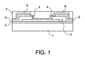
- a bulk wave filter arrangement has a carrier substrate 1 which is, for example, made of a ceramic material, a ceramic material with a planarization layer made of glass, a glass-ceramic material, a glass material, silicon, GaAs or sapphire. If silicon or GaAs is used as the carrier substrate 1, a passivation layer made of, for example, SiO 2 or glass is also applied.
- a first reflection element 2 which is a layer of a sound reflection material from the group of polymeric and porous materials. For example, an airgel, a xerogel, a glass foam, a foam-like adhesive, a foam or a plastic with a low density can be used as the sound reflection material.
- An inorganic airgel made from silica gel or porous SiO 2 structures or an organic airgel such as a resorcinol-formaldehyde airgel, a melamine-formaldehyde airgel or a phenol-formaldehyde airgel can be used as the airgel, for example.
- an inorganic xerogel such as highly condensed polysilicic acid or an organic xerogel such as glue or agar-agar can be used as the xerogel.
- Chemically foamed or physically foamed polymers such as, for example, polystyrene, polycarbonates, polyvinyl chloride, polyurethanes, polyisocyanates, polyisocyanurates, polycarbodiimides, polymethacrylimides, polyacrylimides, acrylic-butadiene-styrene copolymers, polypropylenes or polyesters can be used as foams.
- foamed synthetic resins such as phenol-formaldehyde resins or furan resins, which have a high porosity due to coking, can also be used.
- Two resonator units are applied to the first reflection element 2, each of which contains a first electrode 3, a piezoelectric layer 4 and a second electrode 5.
- the electrodes 3 and 5 are preferably made of a highly conductive material with low acoustic damping and can, for example, Ag 1-x Pt x (0 ⁇ x ⁇ 1), Pt (50 nm to 1 ⁇ m), Ti (1 to 20 nm) / Pt (20 to 600 nm), Ti (1 to 20 nm) / Pt (20 to 600 nm) / Ti (1 to 20 nm), Al, Al doped with a few percent Cu, Al doped with a few percent Si, Al doped with a few percent Mg, W, Ni, Mo, Au, Cu, Ti / Pt / Al, Ti / Ag, Ti / Ag / Ti, Ti / Ag / Ir, Ti / Ir, Ti / Pd, Ti / Ag 1- x Pt x (0 ⁇ x ⁇ 1), Ti / Ag 1-x Pd x (0 ⁇ x ⁇ 1), Ti / Pt 1-x Al x (0 ⁇ x ⁇ 1), P
- a second reflection element 6 which is, for example, a layer made of an airgel, a xerogel, a glass foam, a foam-like adhesive, a foam or a low-density plastic, is applied to parts of the first electrode 3 and second electrode 5 and the piezoelectric layer 4 .
- Alternatives in construction are well known to those skilled in the art.
- a protective layer 7 made of an organic and / or inorganic material is applied over the entire filter arrangement.
- polybenzocyclobutene or polyimide can be used as the organic material and Si 3 N 4 , SiO 2 or Si x O y N z (0 x x 1 1, 0 y y 1 1, 0 z z 1 1), for example, can be used as the inorganic material .
- the reflection elements 2 and 6 can consist of several layers with alternating high and low impedance.
- the material with low impedance can be, for example, an organic or inorganic airgel, an organic or inorganic xerogel, a glass foam, a foam-like adhesive, a foam or a low-density plastic.
- a material with high acoustic impedance for example, HfO 2 , Mo, Au, Ni, Cu, W, Ti / W / Ti, W x Ti 1-x (0 ⁇ x ⁇ 1), diamond, Ta 2 O 5 , Pt, Ti / Pt or a high density plastic such as high density polyethylene (HDPE) can be used.
- HDPE high density polyethylene
- the second reflection element 6 and / or the protective layer 7 can be omitted.
- an additional adhesive layer for example made of an acrylic adhesive or a Epoxy adhesive is applied.
- the acrylate adhesive can, for example, be acrylic or Contain methacrylic monomers that polymerize during the bonding process.
- a layer of SiO 2 with a layer thickness between 30 and 300 nm can be applied above and / or below a reflection element 2 made of porous SiO 2 .
- the filter arrangement with at least a first and a second power supply be provided.
- a galvanic for example, can be used as the power supply SMD end contact made of Cr / Cu, Ni / Sn or Cr / Cu, Cu / Ni / Sn or Cr / Ni, Pb / Sn or a Bump-end contact or a contact surface can be used.
- FIG. 2 shows a filter arrangement comprising a total of nine resonator units M1 to M5 and N1 to N4.
- One connection each four resonator units N1 to N4 are at ground potential.
- the other connector of the resonator unit N1 lies between the resonator units M1 and M2.
- the other connection the resonator unit N2 lies between the resonator units M2 and M3.
- the other The resonator unit N3 is connected between the resonator units M3 and M4.
- the other connection of the resonator unit N4 is between the resonator units M4 and M5.
- a further reflection element 6 can be applied to the second electrode 5 be either a layer of extremely low acoustic impedance material or has several layers with alternating high and low impedance.
- the reflection element 2 has only one layer, which is not necessarily has a layer thickness of a quarter of the resonance wavelength, or more than contains three layers.
- a layer of SiO 2 with a layer thickness between 30 and 300 nm can be applied above and below a reflection element 2 made of porous SiO 2 .
- a protective layer made of an organic and / or inorganic material can be applied over the entire component.
- polybenzocyclobutene or polyimide can be used as the organic material and Si 3 N 4 , SiO 2 or Si x O y N z (0 x x 1 1, 0 y y 1 1, 0 z z 1 1), for example, can be used as the inorganic material .
- an additional adhesive layer for example made of an acrylic adhesive or a Epoxy adhesive applied.
- the acrylate adhesive can, for example, be acrylic or Contain methacrylic monomers that polymerize during the bonding process.
- At least one first can be on opposite sides of the electronic component and a second power supply can be attached.
- a galvanic SMD end contact made of Cr / Cu, Ni / Sn or Cr / Cu, Cu / Ni / Sn or Cr / Ni, Pb / Sn or a bump-end contact or a contact surface can be used.
- a bulk wave resonator can be produced as a component.
- Several of these bulk wave resonators can form a bulk wave filter arrangement can be connected.
- an anti-reaction layer made of TiO 2 , Al 2 O can be placed between the substrate layer 13 and the first electrode 3 3 or ZrO 2 can be applied.
- the reflection element 2 becomes a component directly on the desired carrier substrate 1 deposited.
- the resonator unit then becomes the first electrode 3 and second Electrode 5 and the piezoelectric layer 4 applied.
- the reflection element 2 can alternatively also multiple layers with alternating high and low impedance contain.
- a protective layer 7 made of an organic and / or inorganic material can be applied over the entire component.
- polybenzocyclobutene or polyimide can be used as the organic material and Si 3 N 4 , SiO 2 or Si x O y N z (0 x x 1 1, 0 y y 1 1, 0 z z 1 1), for example, can be used as the inorganic material .
- the further reflection element 6 either has one layer of extremely low acoustic impedance material or more Layers with alternating high and low impedance.
- a layer of SiO 2 with a layer thickness between 30 and 300 nm can be applied above and / or below a reflection element 2 or 6 made of porous SiO 2 .
- At least one first can be on opposite sides of the electronic component and a second power supply can be attached.
- a galvanic SMD end contact made of Cr / Cu, Ni / Sn or Cr / Cu, Cu / Ni / Sn or Cr / Ni, Pb / Sn or a bump-end contact or a contact surface can be used.
- an adhesive layer made of acrylate adhesive was first deposited and then a layer made of porous SiO 2 as a reflection element 2 .
- a first Pt electrode 3 was deposited on a specific part of the reflection element 2.
- a piezoelectric layer 4 made of AlN was applied to certain parts of the first electrode 3 and the reflection element 2.
- a second electrode 5 made of Al was deposited on certain parts of the piezoelectric layer 4 and the reflection element 2.
- the piezoelectric layer 4 and the two electrodes 3, 5 were deposited and structured in such a way that a filter arrangement according to FIG. 2 with a total of 9 resonator units M1 to M5 and N1 to N4 was created.
- resonator units M1 to M5 Five resonator units M1 to M5 were connected in series and the four further resonator units N1 to N4 were connected in parallel to these five resonator units M1 to M5.
- One connection each of the four resonator units N1 to N4 was at ground potential, while the other connections of the resonator units N1 to N4 were each between two of the five resonator units M1 to M5.
- a protective layer 7 made of SiO 2 was applied over the entire filter arrangement. Contact holes to the second electrode 5 were opened through the protective layer 7 by means of etching. Bump-end contacts made of Cr / Cu were grown in the contact holes. The filter arrangement obtained was used as a bandpass filter in mobile telephones.
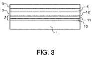
- an adhesive layer made of acrylate adhesive and a lower layer 10 made of porous SiO 2 were first deposited on a glass substrate 1.
- a middle layer 11 of Ta 2 O 5 was deposited on this layer.
- An upper layer 12 made of porous SiO 2 was then applied to the middle layer 11.
- a first electrode 3 made of Mo was deposited on certain parts of the upper layer 12.
- a piezoelectric layer 4 made of AlN was applied to certain parts of the first electrode 3 and the upper layer 12.
- a second electrode 5 made of Al was deposited on certain parts of the piezoelectric layer 4 and the upper layer 12.
- the piezoelectric layer 4 and the two electrodes 3, 5 were deposited and structured in such a way that a filter arrangement according to FIG.
- an adhesive layer made of acrylate adhesive and first a lower layer 10 made of porous SiO 2 was first deposited on a glass substrate 1.
- a middle layer 11 of Ta 2 O 5 was deposited on this layer.
- An upper layer 12 made of porous SiO 2 was then applied to the middle layer 11.
- a first electrode 3 made of Pt and a piezoelectric layer 4 made of PbZr 0.35 Ti 0.65 O 3 were deposited on the upper layer 12.
- a second electrode 5 made of Pt / Ti was applied to the piezoelectric layer 4.
- the entire component was provided with a protective layer made of SiO 2 .
- Cr / Cu, Ni / Sn SMD end contacts were attached as current leads on opposite sides of the component.
- a resonator unit comprising a first electrode 3, a piezoelectric layer 4 and a second electrode 5 was applied to a substrate layer 13 made of Si with a passivation layer made of SiO 2 .
- the first electrode 3 contained Ti / Pt, while the second electrode 5 was made of Pt.
- the piezoelectric layer 4 contained AlN.
- a layer of porous SiO 2 was applied to the second electrode 5 as the reflection element 2 .
- a carrier substrate 1 made of glass with acrylate adhesive was attached to this reflection element 2.
- the Si layer of the substrate layer 13 was then etched away. Contact holes for contacting the first electrode 3 were etched into the remaining SiO 2 layer. Bump-end contacts made of Cr / Cu were then grown in the contact holes.
- a resonator unit comprising a first electrode 3, a piezoelectric layer 4 and a second electrode 5 was applied to a substrate 13 made of Si with a passivation layer made of SiO 2 .
- the first electrode 3 contained Ti / Pt, while the second electrode 5 was made of Pt.
- the piezoelectric layer 4 contained PbZr 0.35 Ti 0.65 O 3 .
- a layer of porous SiO 2 was applied to the second electrode 5 as the reflection element 2 .
- a carrier substrate 1 made of glass with acrylate adhesive was attached to this reflection element 2.
- the Si layer of the substrate 13 was then etched away. Contact holes for contacting the first electrode 3 were etched into the remaining layer of SiO 2 . Bump-end contacts made of Cr / Cu were then grown in the contact holes.
- a resonator unit comprising a first electrode 3, a piezoelectric layer 4 and a second electrode 5 was applied to a substrate 13 made of Si with a passivation layer made of SiO 2 .
- the first electrode 3 contained Ti / Pt and the second electrode 5 contained Pt.
- the piezoelectric layer 4 contained PbZr 0.15 Ti 0.85 O 3 and was produced by means of a centrifugal process.
- a 30 nm thick layer of SiO 2 , a reflection element 2 made of porous SiO 2 and a 300 nm thick layer of SiO 2 were applied to the second electrode 5.
- a carrier substrate 1 made of glass was attached to this structure with an acrylate adhesive.
- the Si layer of the substrate 13 was then etched away. Contact holes for contacting the first electrode 3 were etched into the remaining layer of SiO 2 . Bump-end contacts made of Cr / Cu were then grown in the contact holes.
- a resonator unit comprising a first electrode 3, a piezoelectric layer 4 and a second electrode 5 was applied to a substrate 13 made of Si with a passivation layer made of SiO 2 .
- the first electrode 3 contained Ti / Pt and the second electrode 5 contained W 0.9 Ti 0.1 / Al (Cu).
- the piezoelectric layer 4 contained PbZr 0.35 Ti 0.65 O 3 . and was manufactured using a centrifugal process.
- a 30 nm thick layer of SiO 2 , a reflection element 2 made of porous SiO 2 and a 300 nm thick layer of SiO 2 were applied to the second electrode 5.
- a carrier substrate 1 made of glass was attached to this structure with an acrylate adhesive.
- the Si layer of the substrate 13 was then etched away.
- Contact holes for contacting the first electrode 3 were etched into the remaining layer of SiO 2 .
- Bump-end contacts made of Cr / Cu were then grown in the contact holes.
- a resonator unit comprising a first electrode 3, a piezoelectric layer 4 and a second electrode 5 was applied to a substrate 11 made of Si with a passivation layer made of SiO 2 .
- the first and second electrodes each contained Ti / Pt.
- the piezoelectric layer 4 contained a PLZT layer with the composition PbZr 0 15 Ti 0 85 O 3 with 2% lanthanum doping.
- a 30 nm thick layer of SiO 2 , a reflection element 2 made of porous SiO 2 and a 300 nm thick layer of SiO 2 were applied to the second electrode 5.
- a carrier substrate 1 made of glass was attached to this structure with an acrylate adhesive.
- the Si layer of the substrate 13 was then etched away. Contact holes for contacting the first electrode 3 were etched into the remaining layer of SiO 2 . Bump-end contacts made of Cr / Cu were then grown in the contact holes.
Landscapes
- Physics & Mathematics (AREA)
- Acoustics & Sound (AREA)
- Chemical & Material Sciences (AREA)
- Crystallography & Structural Chemistry (AREA)
- Engineering & Computer Science (AREA)
- Manufacturing & Machinery (AREA)
- Ceramic Engineering (AREA)
- Piezo-Electric Or Mechanical Vibrators, Or Delay Or Filter Circuits (AREA)
- Compositions Of Oxide Ceramics (AREA)
Abstract
Description
Die Erfindung betrifft eine Filteranordnung mit einem Trägersubstrat, einer Resonatoreinheit und einem Reflexionselement zwischen Trägersubstrat und Resonatoreinheit. Die Erfindung betrifft auch ein elektronisches Bauelement mit einem Trägersubstrat, einer Resonatoreinheit und einem Reflexionselement zwischen Trägersubstrat und Resonatoreinheit, sowie ein Verfahren seiner Herstellung.The invention relates to a filter arrangement with a carrier substrate, a resonator unit and a reflection element between the carrier substrate and the resonator unit. The The invention also relates to an electronic component with a carrier substrate, one Resonator unit and a reflection element between the carrier substrate and the resonator unit, and a process for its manufacture.
Die rasanten Entwicklungen im Mobilfunkbereich und die stete Miniaturisierung der schnurlosen Telefonapparate führen zu erhöhten Anforderungen an die einzelnen Komponenten. So ist eine hohe Selektivität im Hochfrequenzteil nötig, um den Empfänger gegen die steigende Anzahl möglicherweise störender Signale von anderen Systeme zu schützen.The rapid developments in the field of mobile communications and the constant miniaturization of cordless telephones lead to increased demands on the individual components. A high selectivity in the high-frequency part is necessary to counter the receiver protect the increasing number of potentially interfering signals from other systems.
Zur Zeit werden im Hochfrequenzbereich für diese Aufgabe Filter mit keramischen, elektromagnetischen Resonatoren verwendet. Einer Miniaturisierung dieser Filter wird aber durch die elektromagnetische Wellenlänge Grenzen gesetzt. Deutlich kleiner können Oberflächenwellen-Filter, sogenannte Surface Acoustic Wave (SAW) Filter, ausgeführt werden. Der Grund hierfür ist, daß die akustische Wellenlänge 4 bis 5 Größenordnungen kleiner ist als die elektromagnetische Wellenlänge. Nachteilig ist aber, daß Oberflächenwellen-Filter oftmals einen komplizierten Aufbau besitzen und mit Hilfe komplexer Gehäuse geschützt werden.At the moment, filters with ceramic, electromagnetic resonators used. Miniaturization of these filters will but is limited by the electromagnetic wavelength. Can be significantly smaller Surface wave filter, so-called surface acoustic wave (SAW) filter, executed become. The reason for this is that the acoustic wavelength is 4 to 5 orders of magnitude is smaller than the electromagnetic wavelength. The disadvantage, however, is that surface wave filters often have a complicated structure and with the help of complex ones Housing are protected.
Eine Alternative stellen Volumenwellen-Filter, die auch als Bulk Acoustic Wave (BAW) Filter bezeichnet werden, dar. Volumenwellen-Filter besitzen Vorteile in den Bereichen Größe, Leistung und IC-Kompatibiität. Volumenwellen-Filter können mit unterschiedlichsten Typen an Volumenwellen-Resonatoren realisiert werden. So können zum Beispiel Einkristall-Resonatoren, Resonatoren mit Membranen oder Resonatoren mit einem Luftspalt verwendet werden. An alternative are volume wave filters, which are also known as bulk acoustic waves (BAW). Filters are referred to. Volume wave filters have advantages in the areas Size, performance and IC compatibility. Bulk wave filters can be used with a wide variety Types of bulk wave resonators can be realized. For example Single crystal resonators, resonators with membranes or resonators with an air gap be used.
Volumenwellen-Resonatoren sind prinzipiell aus drei Komponenten aufgebaut. Die erste Komponente generiert die akustische Welle und enthält eine piezoelektrische Schicht. Zwei Elektroden, welche ober- und unterhalb der piezoelektrischen Schicht angebracht sind, stellen die Zweite Komponente dar. Die dritte Komponente hat die Aufgabe das Trägersubstrat von den Schwingungen, die die piezoelektrische Schicht erzeugt, akustisch zu isolieren.Bulk wave resonators are basically made up of three components. The first Component generates the acoustic wave and contains a piezoelectric layer. Two electrodes, which are attached above and below the piezoelectric layer are the second component. The third component has the task of Carrier substrate from the vibrations that the piezoelectric layer generates, acoustically isolate.
Eine Möglichkeit zur akustischen Isolation stellen Reflexionsschichten dar, die zwischen Trägersubstrat und Resonatoreinheit aufgebracht werden. Solche Reflexionsschichten bestehen aus Schichten mit abwechselnd hoher und niedriger akustischer Impedanz. Die Dicke der einzelnen Schichten beträgt ein Viertel der Resonanzwellenlänge. Diese Schichten haben den Zweck, die akustischen Wellen an den jeweiligen Grenzflächen möglichst gut zu reflektieren und somit die akustische Energie in der Resonatoreinheit zu halten. Die Anzahl der benötigten Schichten richtet sich einerseits nach den Unterschieden in der akustischen Impedanz der einzelnen Schichten und andererseits nach der Resonatorgüte Q, die erreicht werden soll.One possibility for acoustic isolation is provided by reflection layers between Carrier substrate and resonator unit are applied. Such reflection layers exist layers with alternating high and low acoustic impedance. The The thickness of the individual layers is a quarter of the resonance wavelength. These layers have the purpose to avoid the acoustic waves at the respective interfaces reflect well and thus keep the acoustic energy in the resonator unit. The The number of layers required depends on the one hand on the differences in the acoustic impedance of the individual layers and on the other hand according to the resonator quality Q, to be achieved.
Die einzelnen Reflexionsschichten können in den verschiedensten Materialien ausgeführt werden. Als Material mit niedriger akustischer Impedanz wird häufig SiO2 mit einer akustischen Impedanz von 13 Ggm-2s-1 verwendet. AlN mit einer akustischen Impedanz von 34 Ggm-2s-1, W mit einer akustischen Impedanz von 101 Ggm-2s-1 und HfO2 mit einer akustischen Impedanz von 40 Ggm-2s-1 werden als Materialien in Schichten mit hoher akustischer Impedanz verwendet.The individual reflection layers can be made in a wide variety of materials. SiO 2 with an acoustic impedance of 13 Ggm -2 s -1 is often used as the material with low acoustic impedance. AlN with an acoustic impedance of 34 Ggm -2 s -1 , W with an acoustic impedance of 101 Ggm -2 s -1 and HfO 2 with an acoustic impedance of 40 Ggm -2 s -1 are considered to be materials in layers with high acoustic Impedance used.
Aus WO 98/16957 ist ein Volumenwellen-Resonator bekannt, bei dem in den Reflexionsschichten als Materialien mit niedriger akustischer Impedanz Polymere wie zum Beispiel Polyimid zum Einsatz kommen. Durch eine niedrige akustische Impedanz von 2 Ggm-2s-1 kann die Anzahl der zur akustischen Isolation benötigten Reflexionsschichten verringert werden.A bulk wave resonator is known from WO 98/16957, in which polymers such as polyimide are used as materials with low acoustic impedance in the reflection layers. With a low acoustic impedance of 2 Ggm -2 s -1 , the number of reflection layers required for acoustic insulation can be reduced.
Der Erfindung liegt die Aufgabe zugrunde, einen verbesserten Volumenwellen-Filter bereitzustellen. The invention has for its object an improved bulk wave filter to provide.
Diese Aufgabe wird gelöst, durch eine Filteranordnung mit einem Trägersubstrat, einer Resonatoreinheit und einem Reflexionselement zwischen Trägersubstrat und Resonatoreinheit, dadurch gekennzeichnet, daß das Reflexionselement eine Schicht aus einem Schallreflexionsstoff enthält.This object is achieved by a filter arrangement with a carrier substrate, one Resonator unit and a reflection element between the carrier substrate and the resonator unit, characterized in that the reflection element is a layer made of a sound reflection material contains.
Es ist bevorzugt, daß der Schallreflexionsstoff aus der Gruppe der polymeren und porösen Stoffe ist.It is preferred that the sound reflecting material from the group of the polymeric and porous Is fabrics.
Poröse oder polymere Schallreflexionsstoffe besitzen geringe akustische Impedanzen und ermöglichen dadurch, daß nur eine Schicht zur Reflexion der gesamten akustischen Energie nötig ist. In diesem Fall kann sogar auf die Bedingung, daß die Dicke der Schicht ein Viertel der Resonanzwellenlänge beträgt, verzichtet werden. Dies vereinfacht den Aufbau und verbilligt die Herstellung der Filteranordnung.Porous or polymeric sound reflecting materials have low acoustic impedances and thereby allow only one layer to reflect the entire acoustic energy is necessary. In this case, even the condition that the thickness of the layer is a Is a quarter of the resonance wavelength. This simplifies the structure and cheapens the manufacture of the filter arrangement.
Es ist besonders bevorzugt, daß der Schallreflexionsstoff ein Aerogel, ein Xerogel, ein Glasschaum, ein schaumartiger Klebstoff, ein Schaumstoff oder ein Kunststoff mit geringer Dichte ist.It is particularly preferred that the sound reflecting material is an airgel, a xerogel, a glass foam, a foam-like adhesive, a foam or a plastic with less Density is.
Der Vorteil dieser Materialien ist, daß sie extrem geringe Impedanzen von bis zu 10-2 Ggm-2s-1, je nach verwendetem Material, besitzen. Die akustische Impedanz liegt damit im günstigsten Fall nur zwei Größenordnungen über der akustischen Impedanz von Luft (4 · 10-4 Ggm-2s-1).The advantage of these materials is that they have extremely low impedances of up to 10 -2 Ggm -2 s -1 , depending on the material used. At best, the acoustic impedance is only two orders of magnitude above the acoustic impedance of air (4 · 10 -4 Ggm -2 s -1 ).
Es kann bevorzugt sein, daß das Reflexionselement Schichten mit abwechselnd hoher und niedriger Impedanz und als Material für eine Schicht mit niedriger Impedanz einen Schallreflexionsstoff aufweist.It may be preferred that the reflection element layers with alternately high and low impedance and as a material for a layer with low impedance a sound reflecting material having.
Durch die geringen akustischen Impedanzen von polymeren und porösen Schallreflexionsstoffen sind nur sehr wenige Schichten im Reflexionselement nötig, um die gesamte akustische Energie zu reflektieren. Due to the low acoustic impedances of polymeric and porous sound reflecting materials Very few layers are required in the reflection element to cover the entire acoustic Reflect energy.
Es ist bevorzugt, daß das Material mit hoher Impedanz HfO2, Mo, Au, Ni, Cu, W, Ti/W/Ti, WxTi1-x(0 ≤ x ≤ 1), Diamant, Ta2O5, Pt, Ti/Pt oder einen Kunststoff mit hoher Dichte enthält.It is preferred that the high impedance material HfO 2 , Mo, Au, Ni, Cu, W, Ti / W / Ti, W x Ti 1-x (0 ≤ x ≤ 1), diamond, Ta 2 O 5 , Contains Pt, Ti / Pt or a high density plastic.
Die Materialien können mit Dünnschichtverfahren wie reaktivem Sputtern oder Vakuum-Aufdampfverfahren wie zum Beispiel Chemical Vapour Deposition (CVD), Physical Chemical Vapour Deposition (PCVD) oder Spin Coating aufgebracht werden.The materials can be processed using thin film processes such as reactive sputtering or vacuum evaporation such as Chemical Vapor Deposition (CVD), Physical Chemical Vapor Deposition (PCVD) or Spin Coating can be applied.
In dieser Filteranordnung ist es außerdem bevorzugt, daß die Dicke der Schichten jeweils ein Viertel der Resonanzwellenlänge ist.In this filter arrangement it is also preferred that the thickness of the layers in each case is a quarter of the resonance wavelength.
In einer Abfolge von Schichten mit abwechselnd hoher und niedriger Impedanz sowie bei einer Schichtdicke von einem Viertel der Resonanzwellenlänge kombinieren die Reflexionen jeder Schicht bei der Resonanzwellenlänge in Phase.In a sequence of layers with alternating high and low impedance as well as at a layer thickness of a quarter of the resonance wavelength combine the reflections each layer at the resonance wavelength in phase.
Es kann bevorzugt sein, daß ein weiteres Reflexionselement auf der Resonatoreinheit angeordnet ist.It may be preferred that a further reflection element on the resonator unit is arranged.
Das Aufbringen eines weiteren Reflexionselementes auf der Resonatoreinheit hat einerseits den Vorteil, daß keine akustischen Schwingungen an die obere Seite der Filteranordnung gelangen. Andererseits schützen die Reflexionselemente die Resonatoreinheit vor Kontaminierung mit Staubpartikeln oder ähnlichem. Das Aufbringen von Reflexionselementen ober- und unterhalb der Resonatoreinheit, die im günstigsten Fall nur aus einer Schicht bestehen, ist preiswerter als andere Schutztechniken wie beispielsweise eine halbhermetische Packung.The application of a further reflection element on the resonator unit has on the one hand the advantage that no acoustic vibrations on the upper side of the filter arrangement reach. On the other hand, the reflection elements protect the resonator unit from contamination with dust particles or the like. The application of reflection elements Above and below the resonator unit, which in the best case only consists of one layer is cheaper than other protection technologies such as semi-hermetic Pack.
Es ist auch bevorzugt, daß über der Filteranordnung eine Schutzschicht aus einem organischen und/oder anorganischen Material ist.It is also preferred that a protective layer of an organic layer be placed over the filter assembly and / or inorganic material.
Durch die Schutzschicht wird die Filteranordnung vor mechanischer Beanspruchung und Korrosion durch Feuchtigkeit geschützt. The filter arrangement is protected against mechanical stress and the protective layer Corrosion protected by moisture.
Es ist bevorzugt, daß das Trägersubstrat ein keramisches Material, ein keramisches Material mit einer Planarisierungsschicht aus Glas, ein glaskeramisches Material, ein Glasmaterial, Silicium, GaAs oder Saphir enthält.It is preferred that the carrier substrate be a ceramic material, a ceramic material with a planarization layer made of glass, a glass-ceramic material, a glass material, Contains silicon, GaAs or sapphire.
Ein Trägersubstrat aus einem keramischen Material, einem keramischen Material mit einer Planarisierungsschicht aus Glas, einem glaskeramischen Material oder einem Glasmaterial ist kostengünstig herzustellen und die Prozeßkosten für diese Komponente können niedrig gehalten werden. Bei Integration der Filteranordnung in IC's ist das Trägersubstrat aus einem halbleitenden Material gegebenenfalls noch mit einer Passivierungsschicht, beispielsweise SiO2 oder aus Glas, versehen.A carrier substrate made of a ceramic material, a ceramic material with a planarization layer made of glass, a glass-ceramic material or a glass material is inexpensive to manufacture and the process costs for this component can be kept low. When the filter arrangement is integrated in ICs, the carrier substrate made of a semiconducting material is optionally also provided with a passivation layer, for example SiO 2 or made of glass.
Weiterhin ist es bevorzugt, daß die Resonatoreinheit eine piezoelektrische Schicht aus PbZr0.15Ti0.85O3 mit einer 2%igen Lanthan-Dotierung enthält.It is further preferred that the resonator unit contains a piezoelectric layer made of PbZr 0.15 Ti 0.85 O 3 with a 2% lanthanum doping.
PbZr0.15Ti0.85O3 mit einer 2%igen Lanthan-Dotierung weist besonders gute piezoelektrische Eigenschaften in der Filteranordnung auf.PbZr 0.15 Ti 0.85 O 3 with a 2% lanthanum doping has particularly good piezoelectric properties in the filter arrangement.
Es kann bevorzugt sein, daß zwischen Trägersubstrat und Reflexionselement eine Klebstoffschicht ist.It may be preferred that an adhesive layer between the carrier substrate and the reflection element is.
Diese Schicht dient der Befestigung des Reflexionselementes auf dem Trägersubstrat.This layer is used to fasten the reflection element on the carrier substrate.
Außerdem betrifft die Erfindung Mobilfunkgerät, einen Sender, einen Empfänger und ein drahtloses Datenübertragungssystem ausgerüstet mit einer Filteranordnung mit einem Trägersubstrat, einer Resonatoreinheit und einem Reflexionselement zwischen Trägersubstrat und Resonatoreinheit, bei der das Reflexionselement eine Schicht aus einem Schallreflexionsstoff enthält.The invention also relates to a mobile radio device, a transmitter, a receiver and a wireless data transmission system equipped with a filter arrangement with a Carrier substrate, a resonator unit and a reflection element between the carrier substrate and resonator unit, in which the reflection element is a layer of a Contains sound reflection material.
Die Erfindung betrifft auch ein elektronisches Bauelement mit einem Trägersubstrat, einer Resonatoreinheit und einem Reflexionselement zwischen Trägersubstrat und Resonatoreinheit, bei dem das Reflexionselement eine Schicht aus einem Schallreflexionsstoff enthält. The invention also relates to an electronic component with a carrier substrate, one Resonator unit and a reflection element between the carrier substrate and the resonator unit, in which the reflection element contains a layer made of a sound reflection material.
Bei Verwendung von polymeren und porösen Schallreflexionsstoffen mit extrem niedrigen Impedanzen als Reflexionselement können preiswerte Bauelemente, wie zum Beispiel Volumenwellen-Resonatoren, hergestellt werden. Eine Reduktion der Produktionskosten ergibt sich einmal dadurch, daß nur eine Schicht für das Reflexionselement aufgebracht werden muß und außerdem dadurch, daß diese nicht notwendigerweise eine Schichtdicke von einem Viertel der Resonanzwellenlänge aufweisen muß.When using polymeric and porous sound reflecting materials with extremely low Impedances as a reflection element can be inexpensive components, such as Bulk wave resonators are manufactured. A reduction in production costs results from the fact that only one layer is applied for the reflection element and also in that this does not necessarily have a layer thickness must have a quarter of the resonance wavelength.
Weiterhin betrifft die Erfindung ein Verfahren zur Herstellung eines elektronischen Bauelementes mit einem Trägersubstrat, einer Resonatoreinheit und einem Reflexionselement aus einem Schallreflexionsstoff, bei dem
- auf einer Substratschicht eine Resonatoreinheit aufgebracht wird,
- auf der Resonatoreinheit ein Reflexionselement aus einem Schallreflexionsstoff aufgebracht wird,
- auf dem Reflexionselement ein Trägersubstrat befestigt wird und die Substratschicht entfernt wird.
- a resonator unit is applied to a substrate layer,
- a reflection element made of a sound reflection material is applied to the resonator unit,
- a carrier substrate is attached to the reflection element and the substrate layer is removed.
Im folgenden soll die Erfindung anhand von vier Figuren und acht Ausführungsbeispielen erläutert werden. Dabei zeigt
- Fig. 1
- im Querschnitt den Aufbau einer Ausführungsform einer Volumenwellen-Filteranordnung,
- Fig. 2
- die Schaltungsanordnung einer Volumenwellen-Filteranordnung,
- Fig. 3
- im Querschnitt einen Volumenwellen-Resonator mit zwei Reflexionselementen und
- Fig. 4
- ein Fließschema zur Herstellung eines Volumenwellen-Resonators.
- Fig. 1
- in cross section the structure of an embodiment of a bulk wave filter arrangement,
- Fig. 2
- the circuit arrangement of a bulk wave filter arrangement,
- Fig. 3
- in cross section a bulk wave resonator with two reflection elements and
- Fig. 4
- a flow diagram for the manufacture of a bulk wave resonator.
Gemäß Fig. 1 weist eine Volumenwellen-Filteranordnung ein Trägersubstrat 1 auf, welches
zum Beispiel aus einem keramischen Material, einem keramischen Material mit einer
Planarisierungsschicht aus Glas, einem glaskeramischen Material, einem Glasmaterial,
Silicium, GaAs oder Saphir ist. Bei Verwendung von Silicium oder GaAs als Trägersubstrat
1 wird noch eine Passivierungsschicht aus beispielsweise SiO2 oder Glas aufgebracht. Auf
dem Trägersubstrat 1 befindet sich ein erstes Reflexionselement 2, welches eine Schicht
eines Schallreflexionsstoffes aus der Gruppe der polymeren und porösen Stoffe ist. Als
Schallreflexionsstoff kann beispielsweise ein Aerogel, ein Xerogel, ein Glasschaum, ein
schaumartiger Klebstoff, ein Schaumstoff oder ein Kunststoff mit geringer Dichte eingesetzt
werden. Als Aerogel kann zum Beispiel ein anorganisches Aerogel aus Kieselgel oder
porösen SiO2-Strukturen oder ein organisches Aerogel wie zum Beispiel ein Resorcin-Formaldehyd-Aerogel,
ein Melamin-Formaldehyd-Aerogel oder ein Phenol-Formaldehyd-Aerogel
verwendet werden. Als Xerogel kann beispielsweise ein anorganisches Xerogel wie
hochkondensierte Polykieselsäure oder ein organisches Xerogel wie Leim oder Agar-Agar
eingesetzt werden. Als Schaumstoffe können chemisch aufgeschäumte oder physikalisch
aufgeschäumte Polymere wie zum Beispiel Polystyrol, Polycarbonate, Polyvinylchlorid,
Polyurethane, Polyisocyanate, Polyisocyanurate, Polycarbodiimide, Polymethacrylimide,
Polyacrylimide, Acryl-Butadien-Styrol-Copolymere, Polypropylene oder Polyester eingesetzt
werden. Außerdem können auch geschäumte Kunstharze wie beispielsweise Phenol-Formaldehyd-Harze
oder Furanharze, die durch Verkokung eine hohe Porosität besitzen,
verwendet werden. Als Kunststoff mit geringer Dichte kann zum Beispiel ein vernetzter
Polyvinylether, ein vernetzter Polyarylether, Polytetrafluorethylen, Poly(p-xylylen), Poly(2-chlor-p-xylylen),
Poly(dichlor-p-xylylen), Polybenzocyclobuten, ein Styrol-Butadien-Copolymer,
ein Ethylen-Vinylacetat-Polymer oder ein organisches Siloxanpolymer Verwendung
finden. Auf dem ersten Reflexionselement 2 sind zwei Resonatoreinheiten aufgebracht,
welche jeweils eine erste Elektrode 3, eine piezoelektrische Schicht 4 und eine
zweite Elektrode 5 enthalten. Die Elektroden 3 und 5 sind vorzugsweise aus einem gut
leitendem Material mit geringer akustischer Dämpfung und können beispielsweise Ag1-xPtx
(0 ≤ x ≤ 1), Pt (50 nm bis 1 µm), Ti (1 bis 20 nm)/Pt (20 bis 600 nm),
Ti (1 bis 20 nm)/Pt (20 bis 600 nm)/Ti (1 bis 20 nm), Al, Al dotiert mit einigen Prozent
Cu, Al dotiert mit einigen Prozent Si, Al dotiert mit einigen Prozent Mg, W, Ni, Mo, Au,
Cu, Ti/Pt/Al, Ti/Ag, Ti/Ag/Ti, Ti/Ag/Ir, Ti/Ir, Ti/Pd, Ti/Ag1-xPtx
(0 ≤ x ≤ 1), Ti/Ag1-xPdx (0 ≤ x ≤ 1), Ti/Pt1-xAlx (0 ≤ x ≤ 1), Pt1-xAlx (0 ≤ x ≤ 1),
Ti/Ag/Pt1-xAlx (0 ≤ x ≤ 1), Ti/Ag/Ru, Ti/Ag/Ir/IrOx (0 ≤ x ≤ 2), Ti/Ag/Ru/RuOx
(0 ≤ x ≤ 2), Ti/Ag/Ru/RuxPt1-x (0 ≤ x ≤ 1), Ti/Ag/Ru/RuxPt1-x/RuOy (0 ≤ x ≤ 1, 0 ≤ y ≤ 2),
Ti/Ag/Ru/RuOx/RuyPt1-y (0 ≤ x ≤ 2, 0 ≤ y ≤ 1), Ti/Ag/RuxPt1-x (0 ≤ x ≤ 1), Ti/Ag/PtxAl1-x
(0 ≤ x ≤ 1), PtxAl1-x/Ag/PtyAl1-y (0 ≤ x ≤ 1, 0 ≤ y ≤ 1), Ti/Ag/Pty(RhOx)1-y (0 ≤ x ≤ 2,
0 ≤ y ≤ 1), Ti/Ag/Rh/RhOx (0 ≤ x ≤ 2), Ti/Ag/PtxRh1-x (0 ≤ x ≤ 1), Rh, Rh/RhO2,
Ti/Ag/Pty(RhOx)1-y/PtzRh1-z (0 ≤ x ≤ 2, 0 ≤ y ≤ 1, 0 ≤ z ≤ 1), Ti/AgxPt1-x/Ir (0 ≤ x ≤ 1),
Ti/AgxPt1-x/Ir/IrOy (0 ≤ x ≤ 1, 0 ≤ y ≤ 2), Ti/AgxPt1-x/PtyAl1-y (0 ≤ x ≤ 1, 0 ≤ y ≤ 1),
Ti/AgxPt1-x/Ru (0 ≤ x ≤ 1), Ti/AgxPt1-x/Ru/RuOy (0 ≤ x ≤ 1, 0 ≤ y ≤ 2), Ti/Ag/Cr,
Ti/Ag/Ti/ITO, Ti/Ag/Cr/ITO, Ti/Ag/ITO, Ti/Ni/ITO, Ti/Ni/Al/ITO, Ti/Ni, Ti/W/Ti,
WxTi1-x (0 ≤ x ≤ 1), WxTi1-x/Al(Cu) (0 ≤ x ≤ 1), WxTi1-x/Al(Si) (0 ≤ x ≤ 1), WxTi1-x/Al
(0 ≤ x ≤ 1) oder Ti/Cu enthalten. Als Material für die piezoelektrische Schicht 4 kann zum
Beispiel AlN, ZnO, PbTi1-xZrxO3 (O ≤ x ≤ 1) mit und ohne Dotierungen aus La oder Mn,
LiNbO3, LiTaO3, PbNb2O6 oder Polyvinylidenfluorid (PVDF) verwendet werden. Auf
Teilen der ersten Elektrode 3 und zweiten Elektrode 5 sowie der piezoelektrischen Schicht
4 wird ein zweites Reflexionselement 6, welches beispielsweise eine Schicht aus einem
Aerogel, einem Xerogel, einem Glasschaum, einem schaumartigen Klebstoff, einem
Schaumstoff oder einem Kunststoff mit geringer Dichte ist, aufgebracht. Alternativen im
Aufbau sind dem Fachmann wohlbekannt. Über der gesamten Filteranordnung wird eine
Schutzschicht 7 aus einem organischen und/oder anorganischen Material aufgebracht. Als
organisches Material kann beispielsweise Polybenzocyclobuten oder Polyimid und als
anorganisches Material kann zum Beispiel Si3N4, SiO2 oder SixOyNz (0 ≤ x ≤ 1, 0 ≤ y ≤ 1,
0 ≤ z ≤ 1) verwendet werden.1, a bulk wave filter arrangement has a
Alternativ können die Reflexionselemente 2 und 6 aus mehreren Schichten mit abwechselnd
hoher und niedriger Impedanz bestehen. Dabei kann das Material mit niedriger
Impedanz zum Beispiel ein organisches oder anorganisches Aerogel, ein organisches oder
anorganisches Xerogel, ein Glasschaum, ein schaumartiger Klebstoff, ein Schaumstoff oder
ein Kunststoff mit geringer Dichte sein. Als Material mit hoher akustischer Impedanz kann
beispielsweise HfO2, Mo, Au, Ni, Cu, W, Ti/W/Ti, WxTi1-x (0 ≤ x ≤ 1), Diamant, Ta2O5,
Pt, Ti/Pt oder ein Kunststoff mit hoher Dichte wie beispielsweise High-Density-Polyethylen
(HDPE) verwendet werden. Alternatively, the
Ferner kann als weitere Ausführungsform der Erfindung das zweite Reflexionselement 6
und/oder die Schutzschicht 7 weggelassen werden.Furthermore, as a further embodiment of the invention, the
Eine weitere Alternative ist, daß zwischen Reflexionselement 2 und dem Trägersubstrat 1
eine zusätzliche Klebstoffschicht beispielsweise aus einem Acrylat-Klebstoff oder einem
Epoxid-Klebstoff aufgebracht ist. Der Acrylat-Klebstoff kann beispielsweise Acryl- oder
Methacryl-Monomere enthalten, die während des Verklebungsprozeß polymerisieren.Another alternative is that between the
Weiterhin kann ober- und/oder unterhalb eines Reflexionselementes 2 aus porösem SiO2
eine Schicht aus SiO2 mit einer Schichtdicke zwischen 30 und 300 nm aufgebracht sein.Furthermore, a layer of SiO 2 with a layer thickness between 30 and 300 nm can be applied above and / or below a
Außerdem kann die Filteranordnung mit wenigstens einer ersten und einer zweiten Stromzuführung versehen werden. Als Stromzuführung kann beispielsweise ein galvanischer SMD-Endkontakt aus Cr/Cu, Ni/Sn oder Cr/Cu, Cu/Ni/Sn oder Cr/Ni, Pb/Sn oder ein Bump-end-Kontakt oder eine Kontaktflache eingesetzt werden.In addition, the filter arrangement with at least a first and a second power supply be provided. A galvanic, for example, can be used as the power supply SMD end contact made of Cr / Cu, Ni / Sn or Cr / Cu, Cu / Ni / Sn or Cr / Ni, Pb / Sn or a Bump-end contact or a contact surface can be used.
Fig. 2 zeigt eine Filteranordnung aus insgesamt neun Resonatoreinheiten M1 bis M5 sowie
N1 bis N4. Zwischen einem Eingang 8 und einem Ausgang 9 sind fünf Resonatoreinheiten
M1 bis M5 in Serie geschalten. Vier weitere Resonatoreinheiten N1 bis N4 sind
parallel zu diesen fünf Resonatoreinheiten M1 bis M5 geschalten. Jeweils ein Anschluß der
vier Resonatoreinheiten N1 bis N4 liegt auf Erdpotential. Der andere Anschluß der Resonatoreinheit
N1 liegt zwischen den Resonatoreinheiten M1 und M2. Der andere Anschluß
der Resonatoreinheit N2 liegt zwischen den Resonatoreinheiten M2 und M3. Der andere
Anschluß der Resonatoreinheit N3 liegt zwischen den Resonatoreinheiten M3 und M4.
Und der andere Anschluß der Resonatoreinheit N4 liegt zwischen den Resonatoreinheiten
M4 und M5.2 shows a filter arrangement comprising a total of nine resonator units M1 to M5 and
N1 to N4. There are five resonator units between an
Gemäß Fig. 3 weist ein elektronisches Bauelement ein Trägersubstrat 1 auf, welches zum
Beispiel aus einem keramischen Material, einem keramischen Material mit einer Planarisierungsschicht
aus Glas, einem glaskeramischen Material, einem Silicium, GaAs oder Saphir
ist. Bei Verwendung von Silicium oder GaAs als Trägersubstrat 1 wird noch eine Passivierungsschicht
aus beispielsweise SiO2 oder Glas aufgebracht. Auf dem Trägersubstrat 1 ist
ein Reflexionselement 2 mit mehreren Schichten, einer unteren Schicht 10, einer mittleren
Schicht 11 und einer oberen Schicht 12, aufgebracht. Die einzelnen Schichten weisen eine
Schichtdicke von einem Viertel der Resonanzwellenlänge auf. Die untere Schicht 10 und
die obere Schicht 12 sind aus einem Material mit niedriger akustischer Impedanz und
enthalten einen Schallreflexionsstoff aus der Gruppe der polymeren und porösen Stoffe. Als
Schallreflexionsstoff kann beispielsweise ein Aerogel, ein Xerogel, ein Glasschaum, ein
schaumartiger Klebstoff, ein Schaumstoff oder ein Kunststoff mit geringer Dichte eingesetzt
werden. Als Aerogel kann zum Beispiel ein anorganisches Aerogel aus Kieselgel oder
porösen SiO2-Strukturen oder ein organisches Aerogel wie zum Beispiel ein Resorcin-Formaldehyd-Aerogel,
ein Melamin-Formaldehyd-Aerogel oder ein Phenol-Formaldehyd-Aerogel
verwendet werden. Als Xerogel kann beispielsweise ein anorganisches Xerogel wie
hochkondensierte Polykieselsäure oder ein organisches Xerogel wie Leim oder Agar-Agar
eingesetzt werden. Als Schaumstoffe können chemisch aufgeschäumte oder physikalisch
aufgeschäumte Polymere wie zum Beispiel Polystyrol, Polycarbonate, Polyvinylchlorid,
Polyurethane, Polyisocyanate, Polyisocyanurate, Polycarbodiimide, Polymethacrylimide,
Polyacrylimide, Acryl-Butadien-Styrol-Copolymere, Polypropylene oder Polyester eingesetzt
werden. Außerdem können auch geschäumte Kunstharze wie beispielsweise Phenol-Formaldehyd-Harze
oder Furanharze, die durch Verkokung eine hohe Porosität besitzen,
verwendet werden. Als Kunststoff mit geringer Dichte kann zum Beispiel ein vernetzter
Polyvinylether, ein vernetzter Polyarylether, Polytetrafluorethylen, Poly(p-xylylen), Poly(2-chlor-p-xylylen),
Poly(dichlor-p-xylylen), Polybenzocyclobuten, ein Styrol-Butadien-Copolymer,
ein Ethylen-Vinylacetat-Polymer oder ein organisches Polysiloxanpolymer
Verwendung finden. Die akustische Impedanz der mittleren Schicht 11 ist höher als die
akustische Impedanzen der unteren Schicht 10 und der oberen Schicht 12. Die mittlere
Schicht 11 ist aus einem Material mit hoher akustischer Impedanz wie zum Beispiel HfO2,
Mo, Au, Ni, Cu, W, Ti/W/Ti, WxTi1-x, Diamant, Ta2O5, Pt, Ti/Pt oder einem Kunststoff
mit hoher Dichte wie zum Beispiel High-Density-Polyethylen (HDPE). Auf der oberen
Schicht 12 sind eine erste Elektrode 3, eine piezoelektrische Schicht 4 und eine zweite
Elektrode 5 aufgebracht. Die Elektroden 3 und 5 sind vorzugsweise aus einem gut leitenden
Material mit geringer akustischer Dämpfung und können beispielsweise Ag1-xPtx
(0 ≤ x ≤ 1), Pt
(50 nm bis 1 µm), Ti (1 bis 20 nm)/Pt (20 bis 600 nm), Ti (1 bis 20 nm)/Pt
(20 bis 600 nm)/Ti (1 bis 20 nm), Al, Al dotiert mit einigen Prozent Cu, Al dotiert mit
einigen Prozent Si, Al dotiert mit einigen Prozent Mg, Ni, W, Mo, Au, Cu, Ti/Pt/Al,
Ti/Ag, Ti/Ag/Ti, Ti/Ag/Ir, Ti/Ir, Ti/Pd, Ti/Ag1-xPtx (0 ≤ x ≤ 1), Ti/Ag1-xPdx (0 ≤ x ≤ 1),
Ti/Pt1-xAlx (0 ≤ x ≤ 1), Pt1-xAlx (0 ≤ x ≤ 1), Ti/Ag/Pt1-xAlx (0 ≤ x ≤ 1), Ti/Ag/Ru,
Ti/Ag/Ir/IrOx (0 ≤ x ≤ 2), Ti/Ag/Ru/RuOx (0 ≤ x ≤ 2), Ti/Ag/Ru/RuxPt1-x (0 ≤ x ≤ 1),
Ti/Ag/Ru/RuxPt1-x/RuOy (0 ≤ x ≤ 1, 0 ≤ y ≤ 2), Ti/Ag/Ru/RuOx/RuyPt1-y (0 ≤ x ≤ 2,
0 ≤ y ≤ 1), Ti/Ag/RuxPt1-x (0 ≤ x ≤ 1), Ti/Ag/PtxAl1-x (0 ≤ x ≤ 1), PtxAl1-x/Ag/PtyAl1-y
(0 ≤ x ≤ 1, 0 ≤ y ≤ 1),Ti/Ag/Pty(RhOx)1-y (0 ≤ x ≤ 2, 0 ≤ y ≤ 1),Ti/Ag/Rh/RhOx
(0 ≤ x ≤ 2), Ti/Ag/PtxRh1-x (0 ≤ x ≤ 1), Ti/Ag/Pty(RhOx)1-y/PtzRh1-z (0 ≤ x ≤ 2, 0 ≤ y ≤ 1, 0
≤ z ≤ 1), Rh, Rh/RhO2, Ti/AgxPt1-x/Ir (0 ≤ x ≤ 1), Ti/AgxPt1-x/Ir/IrOy (0 ≤ x ≤ 1, 0 ≤ y ≤
2), Ti/AgxPt1-x/PtyAl1-y (0 ≤ x ≤ 1, 0 ≤ y ≤ 1), Ti/AgxPt1-x/Ru (0 ≤ x ≤ 1), Ti/AgxPt1-x/Ru/RuOy
(0 ≤ x ≤ 1, 0 ≤ y ≤ 2), Ti/Ag/Cr, Ti/Ag/Ti/ITO, Ti/Ag/Cr/ITO, Ti/Ag/ITO,
Ti/Ni/ITO, Ti/Ni/Al/ITO, Ti/Ni, Ti/W/Ti, WxTi1-x (0 ≤ x ≤ 1), WxTi1-x/Al(Cu) (0 ≤ x ≤
1), WxTi1-x/Al(Si) (0 ≤ x ≤ 1), WxTi1-x/Al (0 ≤ x ≤ 1) oder Ti/Cu enthalten. Als Material
für die piezoelektrische Schicht 4 kann zum Beispiel AlN, ZnO, PbTi1-xZrxO3 (0 ≤ x ≤ 1)
mit und ohne Dotierungen aus La oder Mn, LiNbO3, LiTaO3, PbNb2O6, Pb1-xCaxTiO3
(0 ≤ x ≤ 1), [Pb(Mg1/3Nb2/3)O3]-PbTiO3]1-x (0 ≤ x ≤ 1), BaTiO3, K1-xNaxNbO3 (0 ≤ x ≤ 1),
(Cd,Na)NbO3, (Bi,Na)TiO3, (Bi,Na,Pb,Ba)TiO3, Bi7Ti4NbO21, (Ba1-xSrx)2NaNb5O15
(0 ≤ x ≤ 1), (Ba1-xSrx)2KNb5O15 (0 ≤ x ≤ 1),
(50 nm to 1 µm), Ti (1 to 20 nm) / Pt (20 to 600 nm), Ti (1 to 20 nm) / Pt (20 to 600 nm) / Ti (1 to 20 nm), Al, Al doped with a few percent Cu, Al doped with a few percent Si, Al doped with a few percent Mg, Ni, W, Mo, Au, Cu, Ti / Pt / Al, Ti / Ag, Ti / Ag / Ti, Ti / Ag / Ir, Ti / Ir, Ti / Pd, Ti / Ag 1-x Pt x (0 ≤ x ≤ 1), Ti / Ag 1-x Pd x (0 ≤ x ≤ 1), Ti / Pt 1-x Al x (0 ≤ x ≤ 1), Pt 1-x Al x (0 ≤ x ≤ 1), Ti / Ag / Pt 1-x Al x (0 ≤ x ≤ 1), Ti / Ag / Ru, Ti / Ag / Ir / IrO x (0 ≤ x ≤ 2), Ti / Ag / Ru / RuO x (0 ≤ x ≤ 2), Ti / Ag / Ru / Ru x Pt 1-x (0 ≤ x ≤ 1), Ti / Ag / Ru / Ru x Pt 1-x / RuO y (0 ≤ x ≤ 1, 0 ≤ y ≤ 2), Ti / Ag / Ru / RuO x / Ru y Pt 1-y (0 ≤ x ≤ 2, 0 ≤ y ≤ 1), Ti / Ag / Ru x Pt 1-x (0 ≤ x ≤ 1), Ti / Ag / Pt x Al 1-x (0 ≤ x ≤ 1), Pt x Al 1-x / Ag / Pt y Al 1-y (0 ≤ x ≤ 1, 0 ≤ y ≤ 1), Ti / Ag / Pt y (RhO x ) 1-y (0 ≤ x ≤ 2, 0 ≤ y ≤ 1), Ti / Ag / Rh / RhO x (0 ≤ x ≤ 2), Ti / Ag / Pt x Rh 1-x (0 ≤ x ≤ 1), Ti / Ag / Pt y (RhO x ) 1-y / Pt z Rh 1-z (0 ≤ x ≤ 2, 0 ≤ y ≤ 1, 0 ≤ z ≤ 1), Rh, Rh / RhO 2 , Ti / Ag x Pt 1-x / Ir (0 ≤ x ≤ 1), Ti / Ag x Pt 1-x / Ir / IrO y (0 ≤ x ≤ 1, 0 ≤ y ≤ 2), Ti / Ag x Pt 1-x / Pt y Al 1-y (0 ≤ x ≤ 1, 0 ≤ y ≤ 1), Ti / Ag x Pt 1-x / Ru (0 ≤ x ≤ 1), Ti / Ag x Pt 1-x / Ru / RuO y (0 ≤ x ≤ 1, 0 ≤ y ≤ 2), Ti / Ag / Cr, Ti / Ag / Ti / ITO, Ti / Ag / Cr / ITO, Ti / Ag / ITO, Ti / Ni / ITO, Ti / Ni / Al / ITO, Ti / Ni, Ti / W / Ti, W x Ti 1-x (0 ≤ x ≤ 1), W x Ti 1-x / Al (Cu) (0 ≤ x ≤ 1), W x Ti 1-x / Al (Si) (0 ≤ x ≤ 1), W x Ti 1-x / Al (0 ≤ x ≤ 1) or Ti / Cu included. As a material for the
Alternativ kann auf der zweiten Elektrode 5 ein weiteres Reflexionselement 6 aufgebracht
werden, das entweder eine Schicht aus einem Material extrem niedriger akustischer Impedanz
oder mehrere Schichten mit abwechselnd hoher und niedriger Impedanz aufweist.Alternatively, a
Es ist auch möglich, daß das Reflexionselement 2 nur eine Schicht, die nicht notwendigerweise
eine Schichtdicke von einem Viertel der Resonanzwellenlänge aufweist, oder mehr als
drei Schichten enthält.It is also possible that the
Ferner kann ober- und unterhalb eines Reflexionselementes 2 aus porösem SiO2 eine
Schicht aus SiO2 mit einer Schichtdicke zwischen 30 und 300 nm aufgebracht sein.Furthermore, a layer of SiO 2 with a layer thickness between 30 and 300 nm can be applied above and below a
Weiterhin kann über dem gesamten Bauelement eine Schutzschicht aus einem organischen
und/oder anorganischen Material aufgebracht werden. Als organisches Material kann beispielsweise
Polybenzocyclobuten oder Polyimid und als anorganisches Material kann zum
Beispiel Si3N4, SiO2 oder SixOyNz (0 ≤ x ≤ 1, 0 ≤ y ≤ 1, 0 ≤ z ≤ 1) verwendet werden.Furthermore, a protective layer made of an organic and / or inorganic material can be applied over the entire component. For example, polybenzocyclobutene or polyimide can be used as the organic material and Si 3 N 4 , SiO 2 or Si x O y N z (0
In einer weiteren Alternative ist zwischen Reflexionselement 2 und dem Trägersubstrat 1
eine zusätzliche Klebstoffschicht, bespielsweise aus einem Acrylat-Klebstoff oder einem
Epoxid-Klebstoff, aufgebracht. Der Acrylat-Klebstoff kann beispielsweise Acryl- oder
Methacryl-Monomere enthalten, die während des Verklebungsprozeß polymerisieren.In a further alternative, there is between the
Auf gegenüberliegenden Seiten des elektronischen Bauelementes kann wenigstens eine erste und eine zweite Stromzuführung angebracht werden. Als Stromzuführung kann beispielsweise ein galvanischer SMD-Endkontakt aus Cr/Cu, Ni/Sn oder Cr/Cu, Cu/Ni/Sn oder Cr/Ni, Pb/Sn oder ein Bump-end-Kontakt oder eine Kontaktfläche eingesetzt werden.At least one first can be on opposite sides of the electronic component and a second power supply can be attached. For example, as a power supply a galvanic SMD end contact made of Cr / Cu, Ni / Sn or Cr / Cu, Cu / Ni / Sn or Cr / Ni, Pb / Sn or a bump-end contact or a contact surface can be used.
Als Bauelement kann beispielsweise ein Volumenwellen-Resonator hergestellt werden. Mehrere dieser Volumenwellen-Resonatoren können zu einer Volumenwellen-Filteranordnung verschaltet werden.For example, a bulk wave resonator can be produced as a component. Several of these bulk wave resonators can form a bulk wave filter arrangement can be connected.
Gemäß Fig. 4 ist eine Möglichkeit ein erfindungsgemäßes elektronisches Bauelement
herzustellen, indem im ersten Schritt auf einer Substratschicht 13 eine Resonatoreinheit,
welche eine erste Elektrode 3, eine piezoelektrische Schicht 4 und eine zweite Elektrode 5
enthält, abgeschieden wird (Verfahrensschritt 1 in Fig. 4). Die Substratschicht 13 kann
zum Beispiel aus einem keramischen Material, einem keramischen Material mit einer
Planarisierungsschicht aus Glas, einem glaskeramischen Material, einem Silicium, GaAs
oder Saphir sein. Bei Verwendung von Silicium oder GaAs in der Substratschicht 13 wird
noch eine Passivierungsschicht aus beispielsweise SiO2 oder Glas aufgebracht. Die Elektroden
3 und 5 sind vorzugsweise aus einem gut leitenden Material mit geringer akustischer
Dämpfung und können beispielsweise Ag1-xPtx (0 ≤ x ≤ 1), Pt
(50 nm bis 1 µm), Ti (1 bis 20 nm)/Pt (20 bis 600 nm), Ti (1 bis 20 nm)/Pt
(20 bis 600 nm)/Ti (1 bis 20 nm), Al, Al dotiert mit einigen Prozent Cu, Al dotiert mit
einigen Prozent Si, Al dotiert mit einigen Prozent Mg, Ni, W, Mo, Au, Cu, Ti/Pt/Al,
Ti/Ag, Ti/Ag/Ti, Ti/Ag/Ir, Ti/Ir, Ti/Pd, Ti/Ag1-xPtx (0 ≤ x ≤ 1), Ti/Ag1-xPdx (0 ≤ x ≤ 1),
Ti/Pt1-xAlx (0 ≤ x ≤ 1), Pt1-xAlx (0 ≤ x ≤ 1), Ti/Ag/Pt1-xAlx (0 ≤ x ≤ 1), Ti/Ag/Ru,
Ti/Ag/Ir/IrOx (0 ≤ x ≤ 2), Ti/Ag/Ru/RuOx (0 ≤ x ≤ 2), Ti/Ag/Ru/RuxPt1-x (0 ≤ x ≤ 1),
Ti/Ag/Ru/RuxPt1-x/RuOy (0 ≤ x ≤ 1, 0 ≤ y ≤ 2), Ti/Ag/Ru/RuOx/RuyPt1-y (0 ≤ x ≤ 2,
0 ≤ y ≤ 1), Ti/Ag/RuxPt1-x (0 ≤ x ≤ 1), Ti/Ag/PtxAl1-x (0 ≤ x ≤ 1), PtxAl1-x/Ag/PtyAl1-y
(0 ≤ x ≤ 1, 0 ≤ y ≤ 1),Ti/Ag/Pty(RhOx)1-y (0 ≤ x ≤ 2, 0 ≤ y ≤ 1),Ti/Ag/Rh/RhOx
(0 ≤ x ≤ 2), Ti/Ag/PtxRh1-x (0 ≤ x ≤ 1), Ti/Ag/Pty(RhOx)1-y/PtzRh1-z (0 ≤ x ≤ 2, 0 ≤ y ≤ 1, 0
≤ z ≤ 1), Rh, Rh/RhO2, Ti/AgxPt1-x/Ir (0 ≤ x ≤ 1), Ti/AgxPt1-x/Ir/IrOy (0 ≤ x ≤ 1, 0 ≤ y ≤
2), Ti/AgxPt1-x/PtyAl1-y (0 ≤ x ≤ 1, 0 ≤ y ≤ 1), Ti/AgxPt1-x/Ru (0 ≤ x ≤ 1), Ti/AgxPt1-x/Ru/RuOy
(0 ≤ x ≤ 1, 0 ≤ y ≤ 2), Ti/Ag/Cr, Ti/Ag/Ti/ITO, Ti/Ag/Cr/ITO, Ti/Ag/ITO,
Ti/Ni/ITO, Ti/Ni/Al/ITO, TI/Ni, Ti/W/Ti, WxTi1-x (0 ≤ x ≤ 1), WxTi1-x/Al(Cu) (0 ≤ x ≤
1), WxTi1-x/Al(Si) (0 ≤ x ≤ 1), WxTi1-x/Al (0 ≤ x ≤ 1) oder Ti/Cu enthalten. Als Material
für die piezoelektrische Schicht 4 kann zum Beispiel AlN, ZnO, PbTi1-xZrxO3 (0 ≤ x ≤ 1)
mit und ohne Dotierungen aus La oder Mn, LiNbO3, LiTaO3, PbNb2O6, Pb1-xCaxTiO3
(0 ≤ x ≤ 1), [Pb(Mg1/3Nb2/3)O3]-PbTiO3]1-x (0 ≤ x ≤ 1), BaTiO3, K1-xNaxNbO3 (0 ≤ x ≤ 1),
(Cd,Na)NbO3, (Bi,Na)TiO3, (Bi,Na,Pb,Ba)TiO3, Bi7Ti4NbO21, (Ba1-xSrx)2NaNb5O15
(0 ≤ x ≤ 1), (Ba1-xSrx)2KNb5O15 (0 ≤ x ≤ 1),
(50 nm to 1 µm), Ti (1 to 20 nm) / Pt (20 to 600 nm), Ti (1 to 20 nm) / Pt (20 to 600 nm) / Ti (1 to 20 nm), Al, Al doped with a few percent Cu, Al doped with a few percent Si, Al doped with a few percent Mg, Ni, W, Mo, Au, Cu, Ti / Pt / Al, Ti / Ag, Ti / Ag / Ti, Ti / Ag / Ir, Ti / Ir, Ti / Pd, Ti / Ag 1-x Pt x (0 ≤ x ≤ 1), Ti / Ag 1-x Pd x (0 ≤ x ≤ 1), Ti / Pt 1-x Al x (0 ≤ x ≤ 1), Pt 1-x Al x (0 ≤ x ≤ 1), Ti / Ag / Pt 1-x Al x (0 ≤ x ≤ 1), Ti / Ag / Ru, Ti / Ag / Ir / IrO x (0 ≤ x ≤ 2), Ti / Ag / Ru / RuO x (0 ≤ x ≤ 2), Ti / Ag / Ru / Ru x Pt 1-x (0 ≤ x ≤ 1), Ti / Ag / Ru / Ru x Pt 1-x / RuO y (0 ≤ x ≤ 1, 0 ≤ y ≤ 2), Ti / Ag / Ru / RuO x / Ru y Pt 1-y (0 ≤ x ≤ 2, 0 ≤ y ≤ 1), Ti / Ag / Ru x Pt 1 - x (0 ≤ x ≤ 1), Ti / Ag / Pt x Al 1-x (0 ≤ x ≤ 1), Pt x Al 1-x / Ag / Pt y Al 1-y (0 ≤ x ≤ 1, 0 ≤ y ≤ 1), Ti / Ag / Pt y (RhO x ) 1-y (0 ≤ x ≤ 2, 0 ≤ y ≤ 1), Ti / Ag / Rh / RhO x (0 ≤ x ≤ 2), Ti / Ag / Pt x Rh 1-x (0 ≤ x ≤ 1), Ti / Ag / Pt y (RhO x ) 1-y / Pt z Rh 1-z (0 ≤ x ≤ 2, 0 ≤ y ≤ 1 , 0 ≤ z ≤ 1), Rh, Rh / RhO 2 , Ti / Ag x Pt 1-x / Ir (0 ≤ x ≤ 1), Ti / Ag x Pt 1-x / Ir / IrO y (0 ≤ x ≤ 1, 0 ≤ y ≤ 2), Ti / Ag x Pt 1-x / Pt y Al 1-y (0 ≤ x ≤ 1, 0 ≤ y ≤ 1), Ti / Ag x Pt 1-x / Ru ( 0 ≤ x ≤ 1), Ti / Ag x Pt 1-x / Ru / RuO y (0 ≤ x ≤ 1, 0 ≤ y ≤ 2), Ti / Ag / Cr, Ti / Ag / Ti / ITO, Ti / Ag / Cr / ITO, Ti / Ag / ITO, Ti / Ni / ITO, Ti / Ni / Al / ITO, TI / Ni, Ti / W / Ti, W x Ti 1-x (0 ≤ x ≤ 1), W x Ti 1-x / Al (Cu) (0 ≤ x ≤ 1), W x Ti 1-x / Al (Si) (0 ≤ x ≤ 1), W x Ti 1-x / Al (0 ≤ x ≤ 1) or Ti / Cu included. As a material for the
Bei Verwendung von PbTi1-xZrxO3 (0 ≤ x ≤ 1) mit und ohne Dotierungen aus La oder Mn
als Material für die piezoelektrische Schicht 4 kann zwischen Substratschicht 13 und erster
Elektrode 3 eine Antireaktionsschicht aus TiO2, Al2O3 oder ZrO2 aufgebracht werden.When using PbTi 1-x Zr x O 3 (0 ≤ x ≤ 1) with and without doping made of La or Mn as material for the
In einem alternativen Verfahren zur Herstellung eines erfindungsgemäßen elektronischen
Bauelementes wird das Reflexionselement 2 direkt auf das gewünschte Trägersubstrat 1
abgeschieden. Anschließend wird die Resonatoreinheit aus erster Elektrode 3 und zweiter
Elektrode 5 sowie der piezoelektrischen Schicht 4 aufgebracht. Das Reflexionselement 2
kann alternativ auch mehrere Schichten mit abwechselnd hoher und niedriger Impedanz
enthalten.In an alternative method for producing an electronic according to the invention
The
In allen Fällen kann über dem gesamten Bauelement eine Schutzschicht 7 aus einem
organischen und/oder anorganischen Material aufgebracht werden. Als organisches
Material kann beispielsweise Polybenzocyclobuten oder Polyimid und als anorganisches
Material kann zum Beispiel Si3N4, SiO2 oder SixOyNz (0 ≤ x ≤ 1, 0 ≤ y ≤ 1, 0 ≤ z ≤ 1)
verwendet werden.In all cases, a protective layer 7 made of an organic and / or inorganic material can be applied over the entire component. For example, polybenzocyclobutene or polyimide can be used as the organic material and Si 3 N 4 , SiO 2 or Si x O y N z (0
Alternativ kann unter- und oberhalb der Resonatoreinheit des Bauelementes ein
Reflexionselement angebracht werden. Das weitere Reflexionsekment 6 weist entweder
eine Schicht aus einem Material extrem niedriger akustischer Impedanz oder mehrere
Schichten mit abwechselnd hoher und niedriger Impedanz auf.Alternatively, one can be located below and above the resonator unit of the component
Reflection element are attached. The
Weiterhin kann ober- und/oder unterhalb eines Reflexionselementes 2 bzw. 6 aus porösem
SiO2 eine Schicht aus SiO2 mit einer Schichtdicke zwischen 30 und 300 nm aufgebracht
sein.Furthermore, a layer of SiO 2 with a layer thickness between 30 and 300 nm can be applied above and / or below a
Auf gegenüberliegenden Seiten des elektronischen Bauelementes kann wenigstens eine erste und eine zweite Stromzuführung angebracht werden. Als Stromzuführung kann beispielsweise ein galvanischer SMD-Endkontakt aus Cr/Cu, Ni/Sn oder Cr/Cu, Cu/Ni/Sn oder Cr/Ni, Pb/Sn oder ein Bump-end-Kontakt oder eine Kontaktfläche eingesetzt werden. At least one first can be on opposite sides of the electronic component and a second power supply can be attached. For example, as a power supply a galvanic SMD end contact made of Cr / Cu, Ni / Sn or Cr / Cu, Cu / Ni / Sn or Cr / Ni, Pb / Sn or a bump-end contact or a contact surface can be used.
Im folgenden werden Ausführungsformen der Erfindung erläutert, die beispielhafte Realisierungsmöglichkeiten darstellen.In the following, embodiments of the invention are explained, the exemplary implementation options represent.
Auf einem Trägersubstrat 1 aus Glas wurde zunächst eine Klebstoffschicht aus Acrylat-Klebstoff
und darauf als Reflexionselement 2 eine Schicht aus porösem SiO2 abgeschieden.
Auf einem bestimmten Teil des Reflexionselementes 2 wurde eine erste Elektrode 3 aus Pt
abgeschieden. Eine piezoelektrische Schicht 4 aus AlN wurde auf bestimmte Teile der
ersten Elektrode 3 und des Reflexionselements 2 aufgebracht. Eine zweite Elektrode 5 aus
Al wurde auf bestimmte Teile der piezoelektrischen Schicht 4 und des Reflexionselements
2 abgeschieden. Die piezoelektrische Schicht 4 und die zwei Elektroden 3, 5 wurden derart
abgeschieden und strukturiert, daß eine Filteranordnung gemäß Fig. 2 mit insgesamt 9
Resonatoreinheiten M1 bis M5 sowie N1 bis N4 enstand. Dabei wurden fünf Resonatoreinheiten
M1 bis M5 in Serie geschalten und die vier weiteren Resonatoreinheiten N1 bis
N4 wurden parallel zu diesen fünf Resonatoreinheiten M1 bis M5 geschalten. Jeweils ein
Anschluß der vier Resonatoreinheiten N1 bis N4 lag auf Erdpotential, während die anderen
Anschlüsse der Resonatoreinheiten N1 bis N4 jeweils zwischen zwei der fünf Resonatoreinheiten
M1 bis M5 lagen. Ober der gesamten Filteranordnung wurde eine Schutzschicht
7 aus SiO2 aufgebracht. Durch die Schutzschicht 7 wurden mittels Ätzens Kontaktlöcher
zur zweiten Elektrode 5 geöffnet. In den Kontaktlöchern wurden Bump-end-Kontakte
aus Cr/Cu aufgewachsen. Die erhaltene Filteranordnung wurde als Bandpassfilter in
Mobiltelefonen eingesetzt.On a
Zur Realisierung einer Filteranordnung mit einem Reflexionselement 2 aus mehreren
Schichten wurde auf einem Trägersubstrat 1 aus Glas zunächst eine Klebstoffschicht aus
Acrylat-Klebstoff und darauf eine untere Schicht 10 aus porösem SiO2 abgeschieden. Auf
diese Schicht wurde eine mittlere Schicht 11 aus Ta2O5 abgeschieden. Eine obere Schicht
12 aus porösem SiO2 wurde anschließend auf die mittlere Schicht 11 aufgebracht. Auf
bestimmte Teile der oberen Schicht 12 wurde eine erste Elektrode 3 aus Mo abgeschieden.
Eine piezoelektrische Schicht 4 aus AlN wurde auf bestimmte Teile der ersten Elektrode 3
und der oberen Schicht 12 aufgebracht. Eine zweite Elektrode 5 aus Al wurde auf bestimmte
Teile der piezoelektrischen Schicht 4 und der oberen Schicht 12 abgeschieden.
Die piezoelektrische Schicht 4 und die zwei Elektroden 3, 5 wurden derart abgeschieden
und strukturiert, daß eine Filteranordnung gemäß Fig. 2 mit insgesamt 9 Resonatoreinheiten
M1 bis M5 sowie N1 bis N4 enstand. Dabei wurden fünf Resonatoreinheiten M1
bis M5 in Serie geschalten und die vier weitere Resonatoreinheiten N1 bis N4 wurden
parallel zu diesen fünf Resonatoreinheiten M1 bis M5 geschalten. Jeweils ein Anschluß der
vier Resonatoreinheiten N1 bis N4 lag auf Erdpotential, während die anderen Anschlüsse
der Resonatoreinheiten N1 bis N4 jeweils zwischen zwei der fünf Resonatoreinheiten M1
bis M5 lagen. Ober die gesamte Filteranordnung wurde eine Schutzschicht 7 aus SiO2
aufgebracht. Durch die Schutzschicht 7 wurden mittels Ätzens Kontaktlöcher zur zweiten
Elektrode 5 geöffnet. In den Kontaktlöchern wurden Bump-end-Kontakte aus Cr/Cu
aufgewachsen. Die erhaltene Filteranordnung wurde als Bandpassfilter in Mobiltelefonen
eingesetzt.In order to implement a filter arrangement with a
Zur Realisierung eines elektronischen Bauelementes mit einem Reflexionselement 2 aus
mehreren Schichten wurde auf einem Trägersubstrat 1 aus Glas zunächst eine Klebstoffschicht
aus Acrylat-Klebstoff und darauf eine untere Schicht 10 aus porösem SiO2 abgeschieden.
Auf diese Schicht wurde eine mittlere Schicht 11 aus Ta2O5 abgeschieden. Eine
obere Schicht 12 aus porösem SiO2 wurde anschließend auf die mittlere Schicht 11 aufgebracht.
Auf die obere Schicht 12 wurde eine erste Elektrode 3 aus Pt und auf letzterer eine
piezoelektrische Schicht 4 aus PbZr0.35Ti0.65O3 abgeschieden. Eine zweite Elektrode 5 aus
Pt/Ti wurde auf der piezoelektrischen Schicht 4 aufgebracht. Das gesamte Bauelement
wurde mit einer Schutzschicht aus SiO2 versehen. Außerdem wurden an gegenüberliegenden
Seiten des Bauteiles Cr/Cu, Ni/Sn SMD-Endkontakte als Stromzuführungen befestigt.In order to realize an electronic component with a
Zur Herstellung eines Volumenwellen-Resonators wurde auf einer Substratschicht 13 aus
Si mit einer Passivierungsschicht aus SiO2 eine Resonatoreinheit aus erster Elektrode 3,
piezoelektrischer Schicht 4 und zweiter Elektrode 5 aufgebracht. Die erste Elektrode 3
enthielt Ti/Pt, während die zweite Elektrode 5 aus Pt war. Die piezoelektrische Schicht 4
enthielt AlN. Im nächsten Schritt wurde auf der zweiten Elektrode 5 als Reflexionselement
2 eine Schicht aus porösem SiO2 aufgebracht. Auf diesem Reflexionselement 2 wurde ein
Trägersubstrat 1 aus Glas mit Acrylat-Klebstoff befestigt. Anschließend wurde die Si-Schicht
der Substratschicht 13 weggeätzt. In die verbliebene SiO2-Schicht wurden Kontaktlöcher
zur Kontaktierung der ersten Elekrode 3 geätzt. Anschließend wurden Bump-end-Kontakte
aus Cr/Cu in den Kontaktlöchern aufgewachsen.To produce a bulk wave resonator, a resonator unit comprising a
Zur Herstellung eines Volumenwellen-Resonators wurde auf einem Substrat 13 aus Si mit
einer Passivierungsschicht aus SiO2 eine Resonatoreinheit aus erster Elektrode 3, piezoelektrischer
Schicht 4 und zweiter Elektrode 5 aufgebracht. Die erste Elektrode 3 enthielt
Ti/Pt, während die zweite Elektrode 5 aus Pt war. Die piezoelektrische Schicht 4 enthielt
PbZr0.35Ti0.65O3. Im nächsten Schritt wurde auf der zweiten Elektrode 5 als Reflexionselement
2 eine Schicht aus porösem SiO2 aufgebracht. Auf diesem Reflexionselement 2
wurde ein Trägersubstrat 1 aus Glas mit Acrylat-Klebstoff befestigt. Anschließend wurde
die Si-Schicht des Substrats 13 weggeätzt. In die verbliebene Schicht aus SiO2 wurden
Kontaktlöcher zur Kontaktierung der ersten Elektrode 3 geätzt. Anschließend wurden
Bump-end-Kontakte aus Cr/Cu in den Kontaktlöchern aufgewachsen.To produce a bulk wave resonator, a resonator unit comprising a
Zur Herstellung eines Volumenwellen-Resonators wurde auf einem Substrat 13 aus Si mit
einer Passivierungsschicht aus SiO2, eine Resonatoreinheit aus einer ersten Elektrode 3,
einer piezoelektrischen Schicht 4 und einer zweiten Elektrode 5 aufgebracht. Die erste
Elektrode 3 enthielt Ti/Pt und die zweite Elektorde 5 enthielt Pt. Die piezoelektrische
Schicht 4 enthielt PbZr0.15Ti0.85O3 und wurde mittels Schleuderverfahren hergestellt. Im
nächsten Schritt wurde auf die zweite Elektrode 5 eine 30 nm dicke Schicht aus SiO2, ein
Reflexionselement 2 aus porösem SiO2 und eine 300 nm dicke Schicht aus SiO2 aufgebracht.
Auf diesen Aufbau wurde ein Trägersubstrat 1 aus Glas mit einem Acrylat-Klebstoff
befestigt. Anschließend wurde die Si-Schicht des Substrats 13 weggeätzt. In die verbliebene
Schicht aus SiO2 wurden Kontaktlöcher zur Kontaktierung der ersten Elektrode 3
geätzt. Anschließend wurden Bump-end Kontakte aus Cr/Cu in den Kontaktlöchern
aufgewachsen.To produce a bulk wave resonator, a resonator unit comprising a
Zur Herstellung eines Volumenwellen-Resonators wurde auf einem Substrate 13 aus Si mit
einer Passivierungsschicht aus SiO2, eine Resonatoreinheit aus einer ersten Elektrode 3,
einer piezoelektrischen Schicht 4 und einer zweiten Elektrode 5 aufgebracht. Die erste
Elektrode 3 enthielt Ti/Pt und die zweite Elektorde 5 enthielt W0.9Ti0.1/Al(Cu). Die piezoelektrische
Schicht 4 enthielt PbZr0.35Ti0.65O3. und wurde mittels Schleuderverfahren hergestellt.
Im nächsten Schritt wurde auf die zweite Elektrode 5 eine 30 nm dicke Schicht
aus SiO2, ein Reflexionselement 2 aus porösem SiO2 und eine 300 nm dicke Schicht aus
SiO2 aufgebracht. Auf diesen Aufbau wurde ein Trägersubstrat 1 aus Glas mit einem
Acrylat-Klebstoff befestigt. Anschließend wurde die Si-Schicht des Substrats 13 weggeätzt.
In die verbliebene Schicht aus SiO2 wurden Kontaktlöcher zur Kontaktierung der ersten
Elektrode 3 geätzt. Anschließend wurden Bump-end Kontakte aus Cr/Cu in den Kontaktlöchern
aufgewachsen.To produce a bulk wave resonator, a resonator unit comprising a
Zur Herstellung eines Volumenwellen-Resonators wurde auf einem Substrate 11 aus Si mit
einer Passivierungsschicht aus SiO2, eine Resonatoreinheit aus einer ersten Elektrode 3,
einer piezoelektrischen Schicht 4 und einer zweiten Elektrode 5 aufgebracht. Die erste und
zweiter Elektrode enthielten jeweils Ti/Pt. Die piezoelektrische Schicht 4 enthielt eine
PLZT Schicht mit der Zusammensetzung PbZr0 15Ti0 85O3 mit 2% Lanthandotierung. Im
nächsten Schritt wurde auf die zweite Elektrode 5 eine 30 nm dicke Schicht aus SiO2, ein
Reflexionselement 2 aus porösem SiO2 und eine 300 nm dicke Schicht aus SiO2 aufgebracht.
Auf diesen Aufbau wurde ein Trägersubstrat 1 aus Glas mit einem Acrylat-Klebstoff
befestigt. Anschließend wurde die Si-Schicht des Substrats 13 weggeätzt. In verbliebene
Schicht aus SiO2 wurden Kontaktlöcher zur Kontaktierung der ersten Elektrode 3
geätzt. Anschließend wurden Bump-end Kontakte aus Cr/Cu in den Kontaktlöchern
aufgewachsen.To produce a bulk wave resonator, a resonator unit comprising a
Claims (18)
dadurch gekennzeichnet,
daß das Reflexionselement (2) eine Schicht aus einem Schallreflexionsstoff enthält.Filter arrangement with a carrier substrate (1), a resonator unit and a reflection element (2) between the carrier substrate (1) and the resonator unit,
characterized by
that the reflection element (2) contains a layer of a sound reflection material.
dadurch gekennzeichnet,
daß der Schallreflexionsstoff aus der Gruppe der polymeren und porösen Stoffe ist.Filter arrangement according to claim 1,
characterized by
that the sound reflection material is from the group of polymeric and porous materials.
dadurch gekennzeichnet,
daß der Schallreflexionsstoff ein Aerogel, ein Xerogel, ein Glasschaum, ein schaumartiger Klebstoff, ein Schaumstoff oder ein Kunststoff mit geringer Dichte ist.Filter arrangement according to claim 1,
characterized by
that the sound reflecting material is an airgel, a xerogel, a glass foam, a foam-like adhesive, a foam or a low-density plastic.
dadurch gekennzeichnet,
daß das Reflexionselement (2) Schichten (10,11,12) mit abwechselnd hoher und niedriger Impedanz und als Material für eine Schicht (10,12) mit niedriger Impedanz einen Schallreflexionsstoff aufweist.Filter arrangement according to claim 1,
characterized by
that the reflection element (2) has layers (10, 11, 12) with alternating high and low impedance and as material for a layer (10, 12) with low impedance, a sound reflection material.
dadurch gekennzeichnet,
daß das Material mit hoher Impedanz HfO2, Mo, Au, Ni, Cu, W, Ti/W/Ti, WxTi1-x (0 ≤ x ≤ 1), Diamant, Ta2O5, Pt, Ti/Pt oder einen Kunststoff mit hoher Dichte enthält. Filter arrangement according to claim 3,
characterized by
that the high impedance material HfO 2 , Mo, Au, Ni, Cu, W, Ti / W / Ti, W x Ti 1-x (0 ≤ x ≤ 1), diamond, Ta 2 O 5 , Pt, Ti / Contains Pt or a high density plastic.
dadurch gekennzeichnet,
daß die Dicke der Schichten (10,11,12) jeweils ein Viertel der Resonanzwellenlange ist.Filter arrangement according to claim 3,
characterized by
that the thickness of the layers (10, 11, 12) is in each case a quarter of the resonance wavelength.
dadurch gekennzeichnet,
daß ein weiteres Reflexionselement (6) auf der Resonatoreinheit angeordnet ist.Filter arrangement according to claim 1,
characterized by
that a further reflection element (6) is arranged on the resonator unit.
dadurch gekennzeichnet,
daß über der Filteranordnung eine Schutzschicht (7) aus einem organischen und/oder anorganischen Material ist.Filter arrangement according to claim 1,
characterized by
that a protective layer (7) made of an organic and / or inorganic material is above the filter arrangement.
dadurch gekennzeichnet,
daß das Trägersubstrat (1) ein keramisches Material, ein keramisches Material mit einer Planarisierungsschicht aus Glas, ein glaskeramisches Material, ein Glasmaterial, Silicium, GaAs oder Saphir enthält.Filter arrangement according to claim 1,
characterized by
that the carrier substrate (1) contains a ceramic material, a ceramic material with a planarization layer made of glass, a glass-ceramic material, a glass material, silicon, GaAs or sapphire.
dadurch gekennzeichnet,
daß die Resonatoreinheit eine piezoelektrische Schicht (4) aus PbZr0.15Ti0.85O3 mit einer 2%igen Lanthan-Dotierung enthält.Filter arrangement according to claim 1,
characterized by
that the resonator unit contains a piezoelectric layer (4) made of PbZr 0.15 Ti 0.85 O 3 with a 2% lanthanum doping.
dadurch gekennzeichnet,
daß ober- und/oder unterhalb eines Reflexionselementes (2,6) eine Schicht aus SiO2 ist. Filter arrangement according to claim 1,
characterized by
that above and / or below a reflection element (2,6) is a layer of SiO 2 .
dadurch gekennzeichnet,
daß zwischen Trägersubstrat (1) und Reflexionselement (2) eine Klebstoffschicht ist.Filter arrangement according to claim 1,
characterized by
that between the carrier substrate (1) and reflection element (2) is an adhesive layer.
dadurch gekennzeichnet,
daß das Reflexionselemnt (2) eine Schicht aus einem Schallreflexionsstoff enthält.Mobile radio device equipped with a filter arrangement with a carrier substrate (1), a resonator unit and a reflection element (2) between the carrier substrate (1) and the resonator unit,
characterized by
that the reflection element (2) contains a layer of a sound reflection material.
dadurch gekennzeichnet,
daß das Reflexionselement (2) eine Schicht aus einem Schallreflexionsstoff enthält.Transmitter equipped with a filter arrangement with a carrier substrate (1), a resonator unit and a reflection element (2) between the carrier substrate (1) and the resonator unit,
characterized by
that the reflection element (2) contains a layer of a sound reflection material.
dadurch gekennzeichnet,
daß das Reflexionselement (2) eine Schicht aus einem Schallreflexionsstoff enthält.Receiver equipped with a filter arrangement with a carrier substrate (1), a resonator unit and a reflection element (2) between the carrier substrate (1) and the resonator unit,
characterized by
that the reflection element (2) contains a layer of a sound reflection material.
dadurch gekennzeichnet,
daß das Reflexionselement (2) eine Schicht aus einem Schallreflexionsstoff enthält. Wireless data transmission system equipped with a filter arrangement with a carrier substrate (1), a resonator unit and a reflection element (2) between the carrier substrate (1) and the resonator unit,
characterized by
that the reflection element (2) contains a layer of a sound reflection material.
dadurch gekennzeichnet,
daß das Reflexionselement (2) eine Schicht aus einem Schallreflexionsstoff enthält.Electronic component with a carrier substrate (1), a resonator unit and a reflection element (2) between the carrier substrate (1) and the resonator unit,
characterized by
that the reflection element (2) contains a layer of a sound reflection material.
Applications Claiming Priority (2)
| Application Number | Priority Date | Filing Date | Title |
|---|---|---|---|
| DE19931297A DE19931297A1 (en) | 1999-07-07 | 1999-07-07 | Bulk wave filter |
| DE19931297 | 1999-07-07 |
Publications (2)
| Publication Number | Publication Date |
|---|---|
| EP1067685A2 true EP1067685A2 (en) | 2001-01-10 |
| EP1067685A3 EP1067685A3 (en) | 2001-06-27 |
Family
ID=7913909
Family Applications (1)
| Application Number | Title | Priority Date | Filing Date |
|---|---|---|---|
| EP00202274A Withdrawn EP1067685A3 (en) | 1999-07-07 | 2000-06-29 | Bulk wave filter |
Country Status (4)
| Country | Link |
|---|---|
| US (1) | US6466105B1 (en) |
| EP (1) | EP1067685A3 (en) |
| JP (1) | JP2001089236A (en) |
| DE (1) | DE19931297A1 (en) |
Cited By (7)
| Publication number | Priority date | Publication date | Assignee | Title |
|---|---|---|---|---|
| WO2003017481A1 (en) * | 2001-08-14 | 2003-02-27 | Koninklijke Philips Electronics N.V. | Filter system with bulk wave resonator |
| WO2003050950A1 (en) * | 2001-12-11 | 2003-06-19 | Epcos Ag | Acoustic mirror with improved reflection |
| WO2004025832A1 (en) | 2002-09-12 | 2004-03-25 | Philips Intellectual Property & Standards Gmbh | Bulk acoustic wave resonator with means for suppression of pass-band ripple in bulk acoustic wave filters |
| US6741145B2 (en) | 2000-11-24 | 2004-05-25 | Nokia Corporation | Filter structure and arrangement comprising piezoelectric resonators |
| WO2007021408A1 (en) * | 2005-08-11 | 2007-02-22 | Maxim Integrated Products, Inc. | Titanium-tungsten alloy based mirrors and electrodes in bulk acoustic wave devices |
| CN109672420A (en) * | 2018-12-18 | 2019-04-23 | 北方民族大学 | The multi-layer piezoelectric substrate and preparation method thereof of magnesium alloy film is set |
| WO2022089841A1 (en) * | 2020-10-30 | 2022-05-05 | RF360 Europe GmbH | Multi mirror stack |
Families Citing this family (81)
| Publication number | Priority date | Publication date | Assignee | Title |
|---|---|---|---|---|
| US6603241B1 (en) * | 2000-05-23 | 2003-08-05 | Agere Systems, Inc. | Acoustic mirror materials for acoustic devices |
| US6814130B2 (en) * | 2000-10-13 | 2004-11-09 | Chien-Min Sung | Methods of making diamond tools using reverse casting of chemical vapor deposition |
| US7132309B2 (en) * | 2003-04-22 | 2006-11-07 | Chien-Min Sung | Semiconductor-on-diamond devices and methods of forming |
| US7011134B2 (en) * | 2000-10-13 | 2006-03-14 | Chien-Min Sung | Casting method for producing surface acoustic wave devices |
| DE10124349A1 (en) * | 2001-05-18 | 2002-12-05 | Infineon Technologies Ag | Piezoelectric resonator device with detuning layer sequence |
| JP3987036B2 (en) * | 2001-11-06 | 2007-10-03 | インフィネオン テクノロジーズ アクチエンゲゼルシャフト | Filter device and manufacturing method thereof |
| US7275292B2 (en) | 2003-03-07 | 2007-10-02 | Avago Technologies Wireless Ip (Singapore) Pte. Ltd. | Method for fabricating an acoustical resonator on a substrate |
| DE10320702B4 (en) | 2003-05-08 | 2018-03-22 | Snaptrack, Inc. | A method of manufacturing an acoustic wave device having improved power compatibility |
| CN100583626C (en) * | 2003-10-06 | 2010-01-20 | Nxp股份有限公司 | Resonator structure and method of producing it |
| US7242270B2 (en) * | 2003-10-30 | 2007-07-10 | Avago Technologies Wireless Ip (Singapore) Pte. Ltd. | Decoupled stacked bulk acoustic resonator-based band-pass filter |
| US7358831B2 (en) | 2003-10-30 | 2008-04-15 | Avago Technologies Wireless Ip (Singapore) Pte. Ltd. | Film bulk acoustic resonator (FBAR) devices with simplified packaging |
| US6946928B2 (en) | 2003-10-30 | 2005-09-20 | Agilent Technologies, Inc. | Thin-film acoustically-coupled transformer |
| US7362198B2 (en) | 2003-10-30 | 2008-04-22 | Avago Technologies Wireless Ip (Singapore) Pte. Ltd | Pass bandwidth control in decoupled stacked bulk acoustic resonator devices |
| US7019605B2 (en) * | 2003-10-30 | 2006-03-28 | Larson Iii John D | Stacked bulk acoustic resonator band-pass filter with controllable pass bandwidth |
| DE602004000851T2 (en) * | 2003-10-30 | 2007-05-16 | Avago Technologies General Ip (Singapore) Pte. Ltd. | Acoustically coupled thin film transformer with two piezoelectric elements having opposite C-axes orientation |
| US7323805B2 (en) * | 2004-01-28 | 2008-01-29 | Kabushiki Kaisha Toshiba | Piezoelectric thin film device and method for manufacturing the same |
| US6963257B2 (en) * | 2004-03-19 | 2005-11-08 | Nokia Corporation | Coupled BAW resonator based duplexers |
| JP2006013839A (en) * | 2004-06-25 | 2006-01-12 | Ube Ind Ltd | Thin film piezo-electric resonator and thin film piezo-electric filter |
| US7615833B2 (en) | 2004-07-13 | 2009-11-10 | Avago Technologies Wireless Ip (Singapore) Pte. Ltd. | Film bulk acoustic resonator package and method of fabricating same |
| JP4820609B2 (en) * | 2004-09-10 | 2011-11-24 | パナソニック株式会社 | Filter module, duplexer, communication device using piezoelectric resonator, and manufacturing method thereof |
| US7388454B2 (en) | 2004-10-01 | 2008-06-17 | Avago Technologies Wireless Ip Pte Ltd | Acoustic resonator performance enhancement using alternating frame structure |
| US8981876B2 (en) | 2004-11-15 | 2015-03-17 | Avago Technologies General Ip (Singapore) Pte. Ltd. | Piezoelectric resonator structures and electrical filters having frame elements |
| JP4693397B2 (en) * | 2004-11-26 | 2011-06-01 | 京セラ株式会社 | Thin film bulk acoustic wave resonator and filter, and communication device |
| US7202560B2 (en) | 2004-12-15 | 2007-04-10 | Avago Technologies Wireless Ip (Singapore) Pte. Ltd. | Wafer bonding of micro-electro mechanical systems to active circuitry |
| EP1829209A1 (en) * | 2004-12-15 | 2007-09-05 | Philips Intellectual Property & Standards GmbH | Thin film acoustic reflector stack |
| US7791434B2 (en) | 2004-12-22 | 2010-09-07 | Avago Technologies Wireless Ip (Singapore) Pte. Ltd. | Acoustic resonator performance enhancement using selective metal etch and having a trench in the piezoelectric |
| US7427819B2 (en) | 2005-03-04 | 2008-09-23 | Avago Wireless Ip Pte Ltd | Film-bulk acoustic wave resonator with motion plate and method |
| US7369013B2 (en) | 2005-04-06 | 2008-05-06 | Avago Technologies Wireless Ip Pte Ltd | Acoustic resonator performance enhancement using filled recessed region |
| US7436269B2 (en) | 2005-04-18 | 2008-10-14 | Avago Technologies Wireless Ip (Singapore) Pte. Ltd. | Acoustically coupled resonators and method of making the same |
| US7934884B2 (en) * | 2005-04-27 | 2011-05-03 | Lockhart Industries, Inc. | Ring binder cover |
| US7443269B2 (en) | 2005-07-27 | 2008-10-28 | Avago Technologies General Ip (Singapore) Pte. Ltd. | Method and apparatus for selectively blocking radio frequency (RF) signals in a radio frequency (RF) switching circuit |
| US7868522B2 (en) | 2005-09-09 | 2011-01-11 | Avago Technologies Wireless Ip (Singapore) Pte. Ltd. | Adjusted frequency temperature coefficient resonator |
| US7391286B2 (en) | 2005-10-06 | 2008-06-24 | Avago Wireless Ip Pte Ltd | Impedance matching and parasitic capacitor resonance of FBAR resonators and coupled filters |
| US7425787B2 (en) | 2005-10-18 | 2008-09-16 | Avago Technologies Wireless Ip (Singapore) Pte. Ltd. | Acoustic galvanic isolator incorporating single insulated decoupled stacked bulk acoustic resonator with acoustically-resonant electrical insulator |
| US7675390B2 (en) | 2005-10-18 | 2010-03-09 | Avago Technologies Wireless Ip (Singapore) Pte. Ltd. | Acoustic galvanic isolator incorporating single decoupled stacked bulk acoustic resonator |
| US7737807B2 (en) | 2005-10-18 | 2010-06-15 | Avago Technologies Wireless Ip (Singapore) Pte. Ltd. | Acoustic galvanic isolator incorporating series-connected decoupled stacked bulk acoustic resonators |
| US7423503B2 (en) | 2005-10-18 | 2008-09-09 | Avago Technologies Wireless Ip (Singapore) Pte. Ltd. | Acoustic galvanic isolator incorporating film acoustically-coupled transformer |
| US7525398B2 (en) | 2005-10-18 | 2009-04-28 | Avago Technologies General Ip (Singapore) Pte. Ltd. | Acoustically communicating data signals across an electrical isolation barrier |
| US7463499B2 (en) | 2005-10-31 | 2008-12-09 | Avago Technologies General Ip (Singapore) Pte Ltd. | AC-DC power converter |
| US7561009B2 (en) | 2005-11-30 | 2009-07-14 | Avago Technologies General Ip (Singapore) Pte. Ltd. | Film bulk acoustic resonator (FBAR) devices with temperature compensation |
| JP4791181B2 (en) * | 2005-12-28 | 2011-10-12 | 京セラ株式会社 | Thin film bulk acoustic wave resonator, filter and communication device including the same, and method for manufacturing thin film bulk acoustic wave resonator |
| US7746677B2 (en) | 2006-03-09 | 2010-06-29 | Avago Technologies Wireless Ip (Singapore) Pte. Ltd. | AC-DC converter circuit and power supply |
| US7479685B2 (en) | 2006-03-10 | 2009-01-20 | Avago Technologies General Ip (Singapore) Pte. Ltd. | Electronic device on substrate with cavity and mitigated parasitic leakage path |
| US20070228876A1 (en) * | 2006-03-31 | 2007-10-04 | Chien-Min Sung | Diamond Frequency Control Devices and Associated Methods |
| JP5096695B2 (en) * | 2006-05-30 | 2012-12-12 | パナソニック株式会社 | Thin film acoustic resonator |
| JP4846477B2 (en) * | 2006-07-26 | 2011-12-28 | パナソニック株式会社 | Method for manufacturing thin film acoustic resonator |
| US7629865B2 (en) | 2006-05-31 | 2009-12-08 | Avago Technologies Wireless Ip (Singapore) Pte. Ltd. | Piezoelectric resonator structures and electrical filters |
| JP2007335977A (en) * | 2006-06-12 | 2007-12-27 | Toshiba Corp | Electron device |
| US7508286B2 (en) | 2006-09-28 | 2009-03-24 | Avago Technologies Wireless Ip (Singapore) Pte. Ltd. | HBAR oscillator and method of manufacture |
| US7846767B1 (en) | 2007-09-06 | 2010-12-07 | Chien-Min Sung | Semiconductor-on-diamond devices and associated methods |
| US7791435B2 (en) | 2007-09-28 | 2010-09-07 | Avago Technologies Wireless Ip (Singapore) Pte. Ltd. | Single stack coupled resonators having differential output |
| US7855618B2 (en) | 2008-04-30 | 2010-12-21 | Avago Technologies Wireless Ip (Singapore) Pte. Ltd. | Bulk acoustic resonator electrical impedance transformers |
| US7732977B2 (en) | 2008-04-30 | 2010-06-08 | Avago Technologies Wireless Ip (Singapore) | Transceiver circuit for film bulk acoustic resonator (FBAR) transducers |
| US8902023B2 (en) | 2009-06-24 | 2014-12-02 | Avago Technologies General Ip (Singapore) Pte. Ltd. | Acoustic resonator structure having an electrode with a cantilevered portion |
| US8248185B2 (en) | 2009-06-24 | 2012-08-21 | Avago Technologies Wireless Ip (Singapore) Pte. Ltd. | Acoustic resonator structure comprising a bridge |
| US20110121916A1 (en) * | 2009-11-24 | 2011-05-26 | Avago Technologies Wireless Ip (Singapore) Pte. Ltd. | Hybrid bulk acoustic wave resonator |
| US8193877B2 (en) | 2009-11-30 | 2012-06-05 | Avago Technologies Wireless Ip (Singapore) Pte. Ltd. | Duplexer with negative phase shifting circuit |
| US8796904B2 (en) | 2011-10-31 | 2014-08-05 | Avago Technologies General Ip (Singapore) Pte. Ltd. | Bulk acoustic resonator comprising piezoelectric layer and inverse piezoelectric layer |
| US9243316B2 (en) | 2010-01-22 | 2016-01-26 | Avago Technologies General Ip (Singapore) Pte. Ltd. | Method of fabricating piezoelectric material with selected c-axis orientation |
| US8962443B2 (en) | 2011-01-31 | 2015-02-24 | Avago Technologies General Ip (Singapore) Pte. Ltd. | Semiconductor device having an airbridge and method of fabricating the same |
| US9136818B2 (en) | 2011-02-28 | 2015-09-15 | Avago Technologies General Ip (Singapore) Pte. Ltd. | Stacked acoustic resonator comprising a bridge |
| US9203374B2 (en) | 2011-02-28 | 2015-12-01 | Avago Technologies General Ip (Singapore) Pte. Ltd. | Film bulk acoustic resonator comprising a bridge |
| US9083302B2 (en) | 2011-02-28 | 2015-07-14 | Avago Technologies General Ip (Singapore) Pte. Ltd. | Stacked bulk acoustic resonator comprising a bridge and an acoustic reflector along a perimeter of the resonator |
| US9154112B2 (en) | 2011-02-28 | 2015-10-06 | Avago Technologies General Ip (Singapore) Pte. Ltd. | Coupled resonator filter comprising a bridge |
| US9148117B2 (en) | 2011-02-28 | 2015-09-29 | Avago Technologies General Ip (Singapore) Pte. Ltd. | Coupled resonator filter comprising a bridge and frame elements |
| US9425764B2 (en) | 2012-10-25 | 2016-08-23 | Avago Technologies General Ip (Singapore) Pte. Ltd. | Accoustic resonator having composite electrodes with integrated lateral features |
| US9048812B2 (en) | 2011-02-28 | 2015-06-02 | Avago Technologies General Ip (Singapore) Pte. Ltd. | Bulk acoustic wave resonator comprising bridge formed within piezoelectric layer |
| US9444426B2 (en) | 2012-10-25 | 2016-09-13 | Avago Technologies General Ip (Singapore) Pte. Ltd. | Accoustic resonator having integrated lateral feature and temperature compensation feature |
| US9525397B2 (en) * | 2011-03-29 | 2016-12-20 | Avago Technologies General Ip (Singapore) Pte. Ltd. | Acoustic resonator comprising acoustic reflector, frame and collar |
| US9484882B2 (en) * | 2013-02-14 | 2016-11-01 | Avago Technologies General Ip (Singapore) Pte. Ltd. | Acoustic resonator having temperature compensation |
| US8575820B2 (en) | 2011-03-29 | 2013-11-05 | Avago Technologies General Ip (Singapore) Pte. Ltd. | Stacked bulk acoustic resonator |
| US9154111B2 (en) | 2011-05-20 | 2015-10-06 | Avago Technologies General Ip (Singapore) Pte. Ltd. | Double bulk acoustic resonator comprising aluminum scandium nitride |
| US20120293278A1 (en) * | 2011-05-20 | 2012-11-22 | Avago Technologies Wireless Ip (Singapore) Pte. Ltd. | Stacked bulk acoustic resonator comprising distributed bragg reflector |
| US9917567B2 (en) | 2011-05-20 | 2018-03-13 | Avago Technologies General Ip (Singapore) Pte. Ltd. | Bulk acoustic resonator comprising aluminum scandium nitride |
| US8350445B1 (en) | 2011-06-16 | 2013-01-08 | Avago Technologies Wireless Ip (Singapore) Pte. Ltd. | Bulk acoustic resonator comprising non-piezoelectric layer and bridge |
| US8922302B2 (en) | 2011-08-24 | 2014-12-30 | Avago Technologies General Ip (Singapore) Pte. Ltd. | Acoustic resonator formed on a pedestal |
| US9246467B2 (en) | 2012-05-31 | 2016-01-26 | Texas Instruments Incorporated | Integrated resonator with a mass bias |
| CN103532510B (en) * | 2013-10-23 | 2016-08-17 | 无锡华普微电子有限公司 | A kind of etching process of SAW device |
| KR102176280B1 (en) * | 2015-12-18 | 2020-11-09 | 삼성전기주식회사 | Acoustic resonator and method for manufacturing same |
| DE102019121804A1 (en) * | 2019-08-13 | 2021-02-18 | RF360 Europe GmbH | Ultra high frequency microacoustic device |
| CN112383287A (en) * | 2020-11-27 | 2021-02-19 | 广东省科学院半导体研究所 | Surface acoustic wave resonator and preparation method thereof |
Family Cites Families (12)
| Publication number | Priority date | Publication date | Assignee | Title |
|---|---|---|---|---|
| JPS56131979A (en) * | 1980-03-19 | 1981-10-15 | Hitachi Ltd | Piezoelectric material for transparent vibrator and transparent vibrator |
| JPS6175614A (en) * | 1984-09-21 | 1986-04-18 | Nec Corp | Manufacture of thin film piezoelectric vibrator |
| US5311095A (en) * | 1992-05-14 | 1994-05-10 | Duke University | Ultrasonic transducer array |
| US5373268A (en) * | 1993-02-01 | 1994-12-13 | Motorola, Inc. | Thin film resonator having stacked acoustic reflecting impedance matching layers and method |
| US5864261A (en) * | 1994-05-23 | 1999-01-26 | Iowa State University Research Foundation | Multiple layer acoustical structures for thin-film resonator based circuits and systems |
| DE4421007A1 (en) * | 1994-06-18 | 1995-12-21 | Philips Patentverwaltung | Electronic component and method for its production |
| JPH0818115A (en) * | 1994-07-04 | 1996-01-19 | Matsushita Electric Ind Co Ltd | Composite piezoelectric device |
| US5646583A (en) * | 1996-01-04 | 1997-07-08 | Rockwell International Corporation | Acoustic isolator having a high impedance layer of hafnium oxide |
| DE19630883A1 (en) * | 1996-07-31 | 1998-02-05 | Philips Patentverwaltung | Component with a capacitor |
| US5873154A (en) * | 1996-10-17 | 1999-02-23 | Nokia Mobile Phones Limited | Method for fabricating a resonator having an acoustic mirror |
| US5872493A (en) * | 1997-03-13 | 1999-02-16 | Nokia Mobile Phones, Ltd. | Bulk acoustic wave (BAW) filter having a top portion that includes a protective acoustic mirror |
| EP0986172B1 (en) * | 1998-09-11 | 2004-12-01 | Texas Instruments Incorporated | An integrated acoustic thin film resonator |
-
1999
- 1999-07-07 DE DE19931297A patent/DE19931297A1/en not_active Withdrawn
-
2000
- 2000-06-29 EP EP00202274A patent/EP1067685A3/en not_active Withdrawn
- 2000-07-05 US US09/610,595 patent/US6466105B1/en not_active Expired - Lifetime
- 2000-07-07 JP JP2000207106A patent/JP2001089236A/en active Pending
Non-Patent Citations (1)
| Title |
|---|
| None * |
Cited By (11)
| Publication number | Priority date | Publication date | Assignee | Title |
|---|---|---|---|---|
| US6741145B2 (en) | 2000-11-24 | 2004-05-25 | Nokia Corporation | Filter structure and arrangement comprising piezoelectric resonators |
| WO2003017481A1 (en) * | 2001-08-14 | 2003-02-27 | Koninklijke Philips Electronics N.V. | Filter system with bulk wave resonator |
| US6975182B2 (en) * | 2001-08-14 | 2005-12-13 | Koninklijke Philips Electronics N.V. | Filter system with bulk wave resonator having a reflection layer composition that varies with the layer thickness |
| CN1541447B (en) * | 2001-08-14 | 2010-04-21 | Nxp股份有限公司 | Filter system with bulk wave resonator |
| WO2003050950A1 (en) * | 2001-12-11 | 2003-06-19 | Epcos Ag | Acoustic mirror with improved reflection |
| US7230509B2 (en) | 2001-12-11 | 2007-06-12 | Epcos Ag | Acoustic mirror |
| WO2004025832A1 (en) | 2002-09-12 | 2004-03-25 | Philips Intellectual Property & Standards Gmbh | Bulk acoustic wave resonator with means for suppression of pass-band ripple in bulk acoustic wave filters |
| WO2007021408A1 (en) * | 2005-08-11 | 2007-02-22 | Maxim Integrated Products, Inc. | Titanium-tungsten alloy based mirrors and electrodes in bulk acoustic wave devices |
| CN109672420A (en) * | 2018-12-18 | 2019-04-23 | 北方民族大学 | The multi-layer piezoelectric substrate and preparation method thereof of magnesium alloy film is set |
| CN109672420B (en) * | 2018-12-18 | 2023-03-31 | 北方民族大学 | Multi-layer piezoelectric substrate provided with magnesium-aluminum alloy film and preparation method thereof |
| WO2022089841A1 (en) * | 2020-10-30 | 2022-05-05 | RF360 Europe GmbH | Multi mirror stack |
Also Published As
| Publication number | Publication date |
|---|---|
| EP1067685A3 (en) | 2001-06-27 |
| JP2001089236A (en) | 2001-04-03 |
| DE19931297A1 (en) | 2001-01-11 |
| US6466105B1 (en) | 2002-10-15 |
Similar Documents
| Publication | Publication Date | Title |
|---|---|---|
| EP1067685A2 (en) | Bulk wave filter | |
| EP1111780A2 (en) | Filter | |
| DE112004001968B4 (en) | Decoupled stacked bulk acoustic resonant band pass filter with controllable passband bandwidth | |
| DE60126033T2 (en) | Thin-film resonator with a columnar structure and increased bandwidth | |
| EP1290790B1 (en) | Tunable filter arrangement | |
| DE112004002068B4 (en) | Temperature Compensated Acoustic Film Volume Resonator (FBAR) devices | |
| DE602004012511T2 (en) | Bandpass filter with bulk acoustic wave resonator stack with adjustable bandwidth | |
| DE60130298T2 (en) | Acoustic resonator | |
| EP1438787B1 (en) | Baw resonator | |
| DE69326880T2 (en) | Frequency selective method and device | |
| DE60115504T2 (en) | FILTER DEVICE | |
| DE10119442B4 (en) | Cavity spanning bottom electrode of a bulk acoustic wave resonator | |
| DE102007000099B4 (en) | Thin film piezoelectric device | |
| WO2003050950A1 (en) | Acoustic mirror with improved reflection | |
| DE10251876A1 (en) | Acoustic reflector for a BAW resonator | |
| DE102007012383B4 (en) | Working with guided bulk acoustic waves component | |
| EP1001531A2 (en) | Surface acoustic wave device | |
| DE69522747T2 (en) | Acoustic surface wave arrangement of diamond LiTaO3 | |
| EP2288912B1 (en) | Arrangement of a piezoacoustic resonator on an acoustic mirror of a substrate, method for the manufacture of the arrangement and use of the arrangement | |
| DE10316716A1 (en) | Component with a piezoelectric functional layer | |
| EP1419577A1 (en) | Filter system with bulk wave resonator | |
| DE102007000100A1 (en) | Piezoelectric thin film device | |
| WO2003043188A1 (en) | Passivated baw resonator and baw filter | |
| DE102018125498B4 (en) | Electroacoustic RF filter with improved performance and multiplexer component that includes an RF filter | |
| DE102018104947B3 (en) | BAW resonator with an increased quality factor |
Legal Events
| Date | Code | Title | Description |
|---|---|---|---|
| PUAI | Public reference made under article 153(3) epc to a published international application that has entered the european phase |
Free format text: ORIGINAL CODE: 0009012 |
|
| AK | Designated contracting states |
Kind code of ref document: A2 Designated state(s): DE FR GB |
|
| AX | Request for extension of the european patent |
Free format text: AL;LT;LV;MK;RO;SI |
|
| PUAL | Search report despatched |
Free format text: ORIGINAL CODE: 0009013 |
|
| AK | Designated contracting states |
Kind code of ref document: A3 Designated state(s): AT BE CH CY DE DK ES FI FR GB GR IE IT LI LU MC NL PT SE |
|
| AX | Request for extension of the european patent |
Free format text: AL;LT;LV;MK;RO;SI |
|
| RIC1 | Information provided on ipc code assigned before grant |
Free format text: 7H 03H 9/58 A, 7H 03H 9/17 B |
|
| 17P | Request for examination filed |
Effective date: 20011227 |
|
| AKX | Designation fees paid |
Free format text: DE FR GB |
|
| RAP1 | Party data changed (applicant data changed or rights of an application transferred) |
Owner name: KONINKLIJKE PHILIPS ELECTRONICS N.V. Owner name: PHILIPS CORPORATE INTELLECTUAL PROPERTY GMBH |
|
| RAP1 | Party data changed (applicant data changed or rights of an application transferred) |
Owner name: PHILIPS INTELLECTUAL PROPERTY & STANDARDS GMBH Owner name: KONINKLIJKE PHILIPS ELECTRONICS N.V. |
|
| 17Q | First examination report despatched |
Effective date: 20061130 |
|
| RAP1 | Party data changed (applicant data changed or rights of an application transferred) |
Owner name: NXP B.V. |
|
| RAP1 | Party data changed (applicant data changed or rights of an application transferred) |
Owner name: TRIQUINT SEMICONDUCTOR, INC. |
|
| STAA | Information on the status of an ep patent application or granted ep patent |
Free format text: STATUS: THE APPLICATION IS DEEMED TO BE WITHDRAWN |
|
| 18D | Application deemed to be withdrawn |
Effective date: 20130102 |