EP1067608B1 - Device and control circuit for a piezoelectric actuator - Google Patents
Device and control circuit for a piezoelectric actuator Download PDFInfo
- Publication number
- EP1067608B1 EP1067608B1 EP00401881A EP00401881A EP1067608B1 EP 1067608 B1 EP1067608 B1 EP 1067608B1 EP 00401881 A EP00401881 A EP 00401881A EP 00401881 A EP00401881 A EP 00401881A EP 1067608 B1 EP1067608 B1 EP 1067608B1
- Authority
- EP
- European Patent Office
- Prior art keywords
- voltage
- ceramic
- current
- control device
- piezoelectric ceramic
- Prior art date
- Legal status (The legal status is an assumption and is not a legal conclusion. Google has not performed a legal analysis and makes no representation as to the accuracy of the status listed.)
- Expired - Lifetime
Links
- 239000000919 ceramic Substances 0.000 claims description 94
- 238000007599 discharging Methods 0.000 claims description 16
- 239000003990 capacitor Substances 0.000 claims description 9
- 238000000034 method Methods 0.000 claims description 9
- 230000000694 effects Effects 0.000 claims description 3
- 230000000630 rising effect Effects 0.000 claims description 3
- 230000001105 regulatory effect Effects 0.000 claims 3
- 230000001276 controlling effect Effects 0.000 claims 2
- 238000002347 injection Methods 0.000 description 15
- 239000007924 injection Substances 0.000 description 15
- 238000010586 diagram Methods 0.000 description 12
- 239000000446 fuel Substances 0.000 description 8
- 230000033228 biological regulation Effects 0.000 description 6
- 230000000903 blocking effect Effects 0.000 description 6
- 238000010719 annulation reaction Methods 0.000 description 3
- 230000007423 decrease Effects 0.000 description 3
- 230000005669 field effect Effects 0.000 description 3
- 238000011084 recovery Methods 0.000 description 3
- 238000001514 detection method Methods 0.000 description 2
- 235000021183 entrée Nutrition 0.000 description 2
- 201000000251 Locked-in syndrome Diseases 0.000 description 1
- 241000287107 Passer Species 0.000 description 1
- 239000003985 ceramic capacitor Substances 0.000 description 1
- 238000002485 combustion reaction Methods 0.000 description 1
- 230000007257 malfunction Effects 0.000 description 1
Images


Classifications
-
- F—MECHANICAL ENGINEERING; LIGHTING; HEATING; WEAPONS; BLASTING
- F02—COMBUSTION ENGINES; HOT-GAS OR COMBUSTION-PRODUCT ENGINE PLANTS
- F02D—CONTROLLING COMBUSTION ENGINES
- F02D41/00—Electrical control of supply of combustible mixture or its constituents
- F02D41/20—Output circuits, e.g. for controlling currents in command coils
- F02D41/2096—Output circuits, e.g. for controlling currents in command coils for controlling piezoelectric injectors
-
- H—ELECTRICITY
- H02—GENERATION; CONVERSION OR DISTRIBUTION OF ELECTRIC POWER
- H02N—ELECTRIC MACHINES NOT OTHERWISE PROVIDED FOR
- H02N2/00—Electric machines in general using piezoelectric effect, electrostriction or magnetostriction
- H02N2/02—Electric machines in general using piezoelectric effect, electrostriction or magnetostriction producing linear motion, e.g. actuators; Linear positioners ; Linear motors
- H02N2/06—Drive circuits; Control arrangements or methods
- H02N2/065—Large signal circuits, e.g. final stages
- H02N2/067—Large signal circuits, e.g. final stages generating drive pulses
-
- H—ELECTRICITY
- H10—SEMICONDUCTOR DEVICES; ELECTRIC SOLID-STATE DEVICES NOT OTHERWISE PROVIDED FOR
- H10N—ELECTRIC SOLID-STATE DEVICES NOT OTHERWISE PROVIDED FOR
- H10N30/00—Piezoelectric or electrostrictive devices
- H10N30/80—Constructional details
- H10N30/802—Drive or control circuitry or methods for piezoelectric or electrostrictive devices not otherwise provided for
Definitions
- the invention relates to a device for controlling a electronically controlled piezoelectric actuator, and more particularly from a fuel injector to piezoelectric stage controlled by the computer electronic injection of the engine, in a motor vehicle, and a method of implementation of this control device.
- FIG. 1 is an electronic diagram of a device for controlling a piezoelectric ceramic 1 equivalent to a capacitance C, associated with a first inductance L 1 for producing an oscillating circuit for charging the ceramic, at twice the voltage supply U s delivered by a DC DC voltage converter 2 DC itself supplied by the low voltage U b of the battery, of the order of 12 volts.
- An N-channel MOSFET transistor T 10 is connected in series with a diode D 10 , between the converter 2 and the terminal of the inductor L 1 opposite the ceramic.
- the transistor T 10 is controlled in all or nothing by the injection computer 3 for example. When the transistor T 10 is driven to be on, the piezoelectric ceramic 1 charges in oscillating mode.
- the voltage U at its terminals is therefore sinusoidal and reaches a maximum equal to twice the output voltage U s of the converter.
- the transistor T 10 is then controlled blocking. The voltage across the ceramic remains constant.
- the discharge of the piezoelectric ceramic is through a second oscillating circuit, consisting of ceramic and a second inductor L 2 connected to ground.
- a second MOSFET transistor T 20 is connected in series with a diode D 20 between the ceramic 1 and the inductor L 2 .
- the transistor T 20 When the transistor T 20 is controlled to be on, the capacity of the ceramic discharges in an oscillating mode through the diode D 20 and the inductance L 2 .
- the diode D 20 is blocked and the transistor T 2 is controlled by the blocking. Then the piezoelectric ceramic remains charged to a negative voltage equal to twice the input voltage.
- Such a device for controlling a piezoelectric ceramic is described in Japanese Patent Application JP 6153538, filed in the name of TOYOTA.
- the oscillating circuit of discharge of the capacity of the piezoelectric ceramic no longer connected to the mass of the converter voltage but at its entrance to ensure cancellation of the voltage across the ceramic and the total recovery of energy.
- the discharge circuit is made up of the same inductance realizing a second oscillating circuit whose voltage input is equal to the input voltage of the voltage converter via a second switch associated with a second diode in series with inductance and passers-by in the direction of discharge current.
- Another object of the invention is a method of control of a piezoelectric ceramic actuator by said device, characterized in that the signal logic driving the switches the device is sent by a control circuit receiving an order of an actuator control calculator, so that the control device operates in a loop open, or in a closed loop, to ensure a complete ceramics.
- the method controls the actuator in regulation mode of the output voltage of the voltage converter according to variations characteristics of the piezoelectric ceramic.
- the method controls the actuator both in regulation mode of the output voltage of the converter according to characteristics of piezoelectric ceramics and more in closed loop to ensure a full charge of this ceramic.
- the control device of a piezoelectric ceramic 10 comprises a converter 11 of the low supply voltage U b , which is that of the battery in the case of a motor vehicle.
- This DC-DC voltage converter DC output a voltage U s which will set the charging voltage of the piezoelectric ceramic.
- the converter provides a voltage of the order of 100 volts for example.
- the converter must be of the uninsulated type, whose negative terminal e - of the input voltage U b is connected to the terminal negative s - of the output voltage U s .
- the charging circuit of the piezoelectric element 10 which is equivalent to an electrical capacitance C, consists on the one hand of an inductance L realizing with the capacitor an oscillating circuit, and on the other hand by a switch T 1 , for example a power transistor, of N-channel MOSFET type, or bipolar or field effect for example, which ensures the charging of the capacitor, associated with a diode D 1 in series with the transistor and the inductance L. It is passing in the direction of the charging current and ensures the end of the charging cycle of this capacity by canceling the current when it is blocked.
- a switch T 1 for example a power transistor, of N-channel MOSFET type, or bipolar or field effect for example
- the discharge circuit of the piezoelectric element is constituted by the same inductance L as the charging circuit for producing a second oscillating circuit, the input voltage of which is equal to the voltage d input U b of the voltage converter 11 via a second switch T 2 , for example a power transistor of the N-channel MOSFET type, the drain of which is connected to a second diode D 2 in series with the terminal the inductor L opposite the piezoelectric element.
- the source of the transistor T 2 is connected to the positive input terminal e + of the converter 11.
- the transistor T 2 discharges the piezoelectric ceramic and the diode D 2 ensures the end of the discharge cycle by canceling the current during its blocking, this transistor and this diode being passing in the direction of the discharge current from the inductor L to the input of the converter.
- the power transistor T 2 may also be bipolar, field effect, or other type.
- first means for maintaining the voltage of the ceramic to a zero value in discharge and current cancellation in inductance L and second means to avoid the burden of ceramic caused by the leakage currents of transistors acting as switches of power.
- these first means consist of a diode D 3 which remains locked until the voltage of the ceramic vanishes
- these second means are constituted by a
- these two means consist of a MOSFET power transistor T 3 , having an internal diode d i .
- This transistor can also be bipolar, field effect, IGBT or other, with a parallel diode whose anode is connected to the ground and the cathode to the inductor.
- the power transistors T 1 and T 2 of the charging and discharging circuits of the piezoelectric element are controlled in all or nothing by a logic signal emitted by an electronic control circuit 12 from an actuator control computer 13, in particular the electronic injection computer for a fuel injector in a vehicle engine.
- the power transistor T 3 is driven by this same logic signal.
- the electronic control computer 13 of the engine emits an injection order which meets the needs of the engine in the amount of fuel required and phased with the position of the engine and the valves, and results in a logic signal S l of the engine circuit.
- the resistor R placed in parallel on the piezoelectric ceramic capacitor C is intended to prevent inadvertent charging of this ceramic because of the leakage currents of the switches. For this, it must have a sufficiently high value determined so that its effect is negligible during the charging and discharging cycles of the piezoelectric ceramic, and to prevent a discharge of this ceramic during the period when it must remain charged.
- the switch T 3 is ignited, in the ON state, before the injection start time t 0 (curve C 3 ) in order to set the voltage at the terminals of the ceramic to a zero value. piezoelectric and produce an effect equivalent to the resistance R.
- the transistor T 2 is kept blocked, only the transistor T 1 being conducting.
- the transistor T 3 is blocked at the time t 0 for detecting the rising edge of the control signal.
- the voltage converter 11 providing a high output voltage U s , a current I, represented by the curve (C 6 ), passes through the oscillating circuit formed by the inductance L and the capacitance C of the ceramic, since the diode D 1 is placed in series with the inductor so as to be busy during the charging of the capacitor C.
- This capacitor C charges up to a theoretical voltage U max equal to twice the output voltage U s of the voltage converter (curve C 5 ).
- the diode D 3 naturally remains blocked and therefore no current I 3 passes through it (curve C 7 ), and the resistance R chosen has a sufficiently high value to neglect its influence in the oscillating circuit during this cycle. loading.
- the transistor T 3 since the transistor T 3 is blocked, its internal diode also remains naturally blocked because the drain-source voltage is positive, so that the transistor T 3 has no influence during the charging of the ceramic .
- FIG. 4 is the equivalent electronic circuit diagram for the charging circuit of the piezoelectric ceramic in the first embodiment.
- the resistor R in parallel with the diode D 3 , by the transistor T 3 to obtain the diagram of the charging circuit in the case of the second embodiment.
- the current I passing through the inductance L is sinusoidal and vanishes at the end time t 1 of the charge cycle of the capacitor C, as does the current I c in the ceramic, represented on curve C 4 .
- Its maximum value is of the order of 15 amperes.
- the current I c also vanishes and the diode D 1 is blocked so that the piezoelectric ceramic remains charged at a constant maximum value U max .
- the electronic circuit 12 controls the blocking of the charge transistor T 1 which returns to the state O.
- the fuel injection sequence by opening the piezoelectric actuator takes place between the charging sequence of the capacity ending at time t 1 and the discharge sequence starting at time t 2 .
- the voltage across the piezoelectric ceramic must be kept constant.
- the power transistors T 1 and T 2 remain locked in the low state to ensure a zero current through the ceramic, between t 1 and t 2 .
- the computer 11 keeps the transistor T 3 blocked to prevent the discharge of this ceramic through it.
- the discharge sequence starts at time t 2 for the control signal from state 1 to state 0.
- the discharge transistor T 2 is immediately initiated and becomes on, while the load transistor T 1 is kept locked in state 0, the voltage between its gate and its source being maintained at zero.
- the transistor T 3 of the second embodiment is kept in the off state, to allow the discharge of the capacitor through the transistor T 2 and the associated diode D 2 .
- the oscillating circuit LC created at the moment of conduction of the discharge transistor T 2 , is connected to the input terminal e + of the voltage converter 11.
- the initial state of the oscillating circuit is different from that of the load since the capacitance is charged and its input voltage is equal to the low voltage of the battery U b . Therefore the voltage across the oscillating circuit will tend neither to a zero value, nor to a negative value, as was the case in the prior art.
- the oscillating discharge of the piezoelectric capacitor C occurs between the instants t 2 and t 3 , that is to say between the detection of the falling edge of the control signal and the cancellation of the voltage across the capacitance. C.
- the current I c in the capacity decreases sinusoidally to zero to a negative value I OC adjacent to the minimum and the current I in the inductor L decreases sinusoidally as from zero to a negative value I 0 equal at I OC .
- the diode D 3 turns on and thus prevents this voltage from becoming negative by keeping it at a value nothing.
- the diode D 3 is the internal diode of the power transistor T 3 which plays the same role.
- FIG. 5 is the electronic diagram equivalent to the discharge circuit of the piezoelectric ceramic in the second variant embodiment. It suffices to replace the transistor T 3 by the resistor R in parallel with the diode D 3 to obtain the diagram of the discharge circuit according to the first embodiment.
- the second sub-sequence starts at time t 3 of cancellation of the voltage U c across the piezoelectric ceramic, while the intensity I of the current in the inductor L is not zero.
- This inductance L is subjected to a positive voltage, equal to the supply voltage U b of the voltage converter 11, which opposes the direction of the current.
- I 0 is the value of current I at time t 3 .
- Figure 6 is the equivalent electronic diagram of circuit for canceling the current in the inductor L, under constant tension.
- the diodes D 2 and D 3 , or D 2 and the internal diode of the transistor T 3 naturally lock, thus preventing the change of direction of the current.
- the discharge transistor T 2 is controlled by the blocking.
- the resistance R avoids the ceramic load caused by leakage currents of the switches.
- the transistor T 3 is driven at ignition to ensure a zero voltage across the piezoelectric ceramic.
- the switches T 1 , T 2 and T 3 are controlled by the electronic control circuit 12 in open loop, from the control signal of a motor control computer by example.
- the device for controlling a piezoelectric actuator operates in open loop, the circuit of command 12 just receiving a signal from the electronic computer for controlling the transistors.
- the device operates in a closed loop in order to adjust the output voltage U s of the DC-DC voltage converter 11 in order to ensure a complete charge of the piezoelectric ceramic.
- the control circuit 12 receives in input, in addition to an order of the control computer 13 of the actuator, the information on the current I flowing through the inductor L and on the voltage U c across the terminals. ceramic. This mode of operation can be applied to both embodiments of the device.
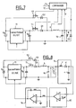
- Figure 7 is an electronic schematic of the second mode closed loop operation of the control according to the invention, applied to the first variant embodiment.
- the control device operates in regulation mode of the voltage of the voltage converter 11, in function of the variations in the characteristics of the piezo ceramic that this regulation be analog or digital.
- the regulation circuit has three elements, as shown in Figure 8 which corresponds to the second variant embodiment.
- a peak detector 14 is connected in parallel on the piezoelectric ceramic C, intended to control the value of its electric charge. It is consisting for example of a resistance r in series with a diode d, associated with a capacitance c connected to the mass.
- the peak detector 14 delivers an output signal to the input of a comparator 15, for comparing the maximum voltage reached across the ceramic with a reference voltage V ref .
- the device can both regulate the output voltage of the voltage converter 11 to take into account variations in the characteristics of this element in time and operate in a closed loop to ensure a total charge of the piezoelectric element.
- FIG. 9 is an electronic diagram of the control device according to this fourth mode of operation, produced according to the second variant with the transistor T 3 .
- the invention has the advantage of completely unloading the piezoelectric ceramic of the actuator, ensuring thus a good functioning of the actuator. Moreover, it ensures the recovery of electrical energy stored in piezoelectric ceramics.
Description
L'invention concerne un dispositif de commande d'un actuateur piézo-électrique piloté électroniquement, et plus particulièrement d'un injecteur de carburant à étage piézo-électrique piloté par le calculateur d'injection électronique du moteur thermique, dans un véhicule automobile, et un procédé de mise en oeuvre de ce dispositif de commande.The invention relates to a device for controlling a electronically controlled piezoelectric actuator, and more particularly from a fuel injector to piezoelectric stage controlled by the computer electronic injection of the engine, in a motor vehicle, and a method of implementation of this control device.
Actuellement, l'injection d'essence ou de gasole dans les cylindres d'un moteur thermique, pour véhicule automobile, est assurée par des injecteurs à céramique piézo-électrique aux bornes de laquelle on fait varier la tension de façon à modifier son épaisseur, entre deux positions extrêmes, ce qui a pour conséquence d'ouvrir et de fermer l'injecteur. La céramique piézo-électrique est équivalente à une capacité, qui est classiquement associée à une inductance pour constituer un circuit oscillant.Currently, the injection of gasoline or diesel into the cylinders of a combustion engine, for a vehicle automotive, is provided by ceramic injectors piezoelectric at the terminals of which is varied the tension so as to modify its thickness, between two extreme positions, which has the consequence to open and close the injector. Piezoelectric ceramics is equivalent to a capacity, which is classically associated with an inductance to constitute an oscillating circuit.
La figure 1 est un schéma électronique d'un dispositif
de commande d'une céramique piézo-électrique 1
équivalente à une capacité C, associée à une première
inductance L1 pour réaliser un circuit oscillant de
charge de la céramique, au double de la tension
d'alimentation Us délivrée par un convertisseur 2 de
tension en courant continu DC-DC alimenté lui-même par
la basse tension Ub de la batterie, de l'ordre de 12
volts. Un transistor T10 de type MOSFET canal N est
branché en série avec une diode D10, entre le
convertisseur 2 et la borne de l'inductance L1 opposée
à la céramique. Le transistor T10 est piloté en tout ou
rien par le calculateur d'injection 3 par exemple.
Lorsque le transistor T10 est piloté pour être passant,
la céramique piézo-électrique 1 se charge en mode
oscillant. La tension U à ses bornes est donc
sinusoïdale et atteint un maximum égal au double de la
tension Us de sortie du convertisseur. Lorsque cette
tension maximale est atteinte aux bornes de la
céramique, le courant qui la traverse s'annule et la
diode D10 se bloque, le transistor T10 est alors
commandé au blocage. La tension aux bornes de la
céramique reste constante.FIG. 1 is an electronic diagram of a device for controlling a
La décharge de la céramique piézo-électrique se fait à
travers un second circuit oscillant, composé de la
céramique et d'une seconde inductance L2 branchée à la
masse. Un second transistor T20 de type MOSFET est
branché en série avec une diode D20 entre la céramique
1 et l'inductance L2. Lorsque le transistor T20 est
commandé pour être passant, la capacité de la céramique
se décharge sous un mode oscillant à travers la diode
D20 et l'inductance L2. Lorsque le courant dans la
capacité s'annule, la diode D20 se bloque et le
transistor T2 est commandé au blocage. Alors la
céramique piézo-électrique reste chargée à une tension
négative égale au double de la tension d'entrée. Un tel
dispositif de commande d'une céramique piézo-électrique
est décrit dans la demande de brevet japonais
JP 6153538, déposée au nom de TOYOTA.The discharge of the piezoelectric ceramic is through a second oscillating circuit, consisting of ceramic and a second inductor L 2 connected to ground. A second MOSFET transistor T 20 is connected in series with a diode D 20 between the
Cette conception actuelle d'un dispositif de commande présente, comme principal inconvénient, la non annulation de la tension aux bornes de la céramique piézo-électrique à la fin du cycle de décharge, en raison des pertes mécaniques dans l'injecteur et des pertes résistives du circuit électrique. Cela pose deux problèmes, d'une part la totalité de l'énergie n'est pas récupérée, et d'autre part la présence d'une charge négative à la fin du cycle de décharge entraíne un mauvais fonctionnement de l'injecteur à céramique.This current design of a control device present, as the main disadvantage, the non cancellation of the voltage across the ceramic piezoelectric at the end of the discharge cycle, because of mechanical losses in the injector and resistive losses of the electrical circuit. This poses two problems, on the one hand the totality of energy is not recovered, and secondly the presence of a charge negative at the end of the discharge cycle leads to a malfunction of the ceramic injector.
Pour pallier ces inconvénients, le circuit oscillant de décharge de la capacité de la céramique piézo-électrique n'est plus relié à la masse du convertisseur de tension, mais à son entrée pour assurer l'annulation de la tension aux bornes de la céramique et la récupération totale de l'énergie.To overcome these disadvantages, the oscillating circuit of discharge of the capacity of the piezoelectric ceramic no longer connected to the mass of the converter voltage but at its entrance to ensure cancellation of the voltage across the ceramic and the total recovery of energy.
Pour cela, l'objet de l'invention est un dispositif de commande d'un actuateur à céramique piézo-électrique, piloté électroniquement par un signal logique, comprenant un convertisseur de tension en courant continu alimenté en basse tension, un circuit de charge de la céramique piézo-électrique constitué d'une inductance réalisant un circuit oscillant avec la capacité de la céramique, en série avec un interrupteur et une diode, caractérisé en ce que :
- le circuit de décharge de la céramique piézo-électrique
est constitué d'une inductance réalisant
un second circuit oscillant dont la tension d'entrée
est égale à la tension d'entrée du convertisseur de
tension par l'intermédiaire d'un second interrupteur
associé à une seconde diode en série avec
l'inductance et passants dans le sens du courant de
décharge, et en ce qu'il comporte:
- des premiers moyens de maintien de la tension aux bornes de la céramique piézo-électrique à une valeur nulle en fin de décharge et d'annulation du courant dans l'inductance, et
- des seconds moyens de blocage de la charge de l'élément piézo-électrique par des courants de fuite des interrupteurs après sa décharge (revendication 1).
- the discharge circuit of the piezoelectric ceramic consists of an inductance producing a second oscillating circuit whose input voltage is equal to the input voltage of the voltage converter via a second switch associated with a second diode in series with the inductor and passers in the direction of the discharge current, and in that it comprises:
- first means for maintaining the voltage across the piezoelectric ceramic at a zero value at the end of the discharge and for canceling the current in the inductor, and
- second means for blocking the charge of the piezoelectric element by leakage currents of the switches after discharge (claim 1).
Selon une autre caractéristique de l'invention, le circuit de décharge est constitué de la même inductance réalisant un second circuit oscillant dont la tension d'entrée est égale à la tension d'entrée du convertisseur de tension par l'intermédiaire d'un second interrupteur associé à une seconde diode en série avec l'inductance et passants dans le sens du courant de décharge.According to another characteristic of the invention, the discharge circuit is made up of the same inductance realizing a second oscillating circuit whose voltage input is equal to the input voltage of the voltage converter via a second switch associated with a second diode in series with inductance and passers-by in the direction of discharge current.
Un autre objet de l'invention est un procédé de commande d'un actuateur à céramique piézo-électrique par ledit dispositif, caractérisé en ce que le signal logique pilotant les interrupteurs du dispositif est envoyé par un circuit de commande recevant un ordre d'un calculateur de contrôle de l'actuateur, de sorte que le dispositif de commande fonctionne soit en boucle ouverte, soit en boucle fermée, pour assurer une charge complète de la céramique.Another object of the invention is a method of control of a piezoelectric ceramic actuator by said device, characterized in that the signal logic driving the switches the device is sent by a control circuit receiving an order of an actuator control calculator, so that the control device operates in a loop open, or in a closed loop, to ensure a complete ceramics.
Selon une autre caractéristique, le procédé commande l'actuateur en mode régulation de la tension de sortie du convertisseur de tension en fonction des variations des caractéristiques de la céramique piézo-électrique.According to another characteristic, the method controls the actuator in regulation mode of the output voltage of the voltage converter according to variations characteristics of the piezoelectric ceramic.
Selon une autre caractéristique, le procédé commande l'actuateur à la fois en mode de régulation de la tension de sortie du convertisseur en fonction des caractéristiques de la céramique piézo-électrique et de plus en boucle fermée pour assurer une charge complète de cette céramique. According to another characteristic, the method controls the actuator both in regulation mode of the output voltage of the converter according to characteristics of piezoelectric ceramics and more in closed loop to ensure a full charge of this ceramic.
D'autres caractéristiques et avantages de l'invention apparaítront à la lecture de la description de deux versions d'un dispositif de commande d'un actuateur piézo-électrique, illustrée par les figures suivantes qui, outre la figure 1 déjà décrite concernant un dispositif de l'art antérieur, sont :
- la figure 2 : une première variante du dispositif de commande d'une céramique piézo-électrique, en boucle ouverte, selon l'invention ;
- la figure 3 : une deuxième variante du dispositif de commande d'une céramique piézo-électrique, en boucle ouverte, selon l'invention ;
- la figure 4 : le schéma équivalent au circuit de charge de la céramique piézo-électrique, selon l'invention ;
- la figure 5 : le schéma équivalent au circuit de décharge de la céramique piézo-électrique, selon l'invention ;
- la figure 6 : le schéma équivalent au circuit d'annulation du courant dans l'inductance du dispositif selon l'invention ;
- les figures 7 et 9 : trois modes de fonctionnement différents du dispositif de commande d'une céramique piézo-électrique, en mode de régulation, selon l'invention ;
- la figure 10 : les courbes d'intensité de courant et de tension lors de la charge puis de la décharge d'une céramique piézo-électrique, selon l'invention.
- Figure 2: a first variant of the control device of a piezoelectric ceramic, open loop, according to the invention;
- Figure 3: a second variant of the control device of a piezoelectric ceramic, open loop, according to the invention;
- FIG. 4: the diagram equivalent to the load circuit of the piezoelectric ceramic, according to the invention;
- Figure 5: the diagram equivalent to the discharge circuit of the piezoelectric ceramic, according to the invention;
- FIG. 6: the diagram equivalent to the current cancellation circuit in the inductance of the device according to the invention;
- FIGS. 7 and 9 show three different modes of operation of the control device of a piezoelectric ceramic, in regulation mode, according to the invention;
- FIG. 10: current and voltage intensity curves during charging and then discharging a piezoelectric ceramic, according to the invention.
Les éléments portant les mêmes références sur les différentes figures remplissent les mêmes fonctions en vue des mêmes résultats. Elements bearing the same references on different figures fulfill the same functions in view of the same results.
Comme le montre le schéma électronique de la figure 2,
le dispositif de commande d'une céramique piézo-électrique
10 selon l'invention comporte un
convertisseur 11 de la basse tension d'alimentation Ub,
qui est celle de la batterie dans le cas d'un véhicule
automobile. Ce convertisseur de tension DC-DC en
courant continu délivre en sortie une tension Us qui
fixera la tension de charge de la céramique piézo-électrique.
Pour une tension d'alimentation de 12
volts, le convertisseur fournit une tension de l'ordre
de 100 volts par exemple. Pour obtenir la récupération
complète de l'énergie stockée lors de la charge de
l'élément piézo-électrique, le convertisseur doit être
de type sans isolation, dont la borne négative e- de la
tension d'entrée Ub est reliée à la borne négative s-
de la tension de sortie Us.As shown in the electronic diagram of FIG. 2, the control device of a
Le circuit de charge de l'élément piézo-électrique 10,
qui est équivalent à une capacité électrique C, est
constitué d'une part par une inductance L réalisant
avec la capacité un circuit oscillant, et d'autre part
par un interrupteur T1, par exemple un transistor de
puissance, de type MOSFET canal N, ou bipolaire ou à
effet de champ par exemple, qui assure la charge de la
capacité, associé à une diode D1 en série avec le
transistor et l'inductance L. Elle est passante dans le
sens du courant de charge et assure la fin du cycle de
charge de cette capacité par annulation du courant lors
de son blocage.The charging circuit of the
Selon une caractéristique de l'invention, le circuit de
décharge de l'élément piézo-électrique est constitué
par la même inductance L que le circuit de charge pour
réaliser un second circuit oscillant, dont la tension
d'entrée est égale à la tension d'entrée Ub du
convertisseur de tension 11 par l'intermédiaire d'un
deuxième interrupteur T2, par exemple un transistor de
puissance, de type MOSFET canal N, dont le drain est
relié à une deuxième diode D2 en série avec la borne de
l'inductance L opposée à l'élément piézo-électrique. La
source du transistor T2 est reliée à la borne positive
e+ d'entrée du convertisseur 11. Le transistor T2
assure la décharge de la céramique piézo-électrique et
la diode D2 assure la fin du cycle de décharge par
annulation du courant lors de son blocage, ce
transistor et cette diode étant passants dans le sens
du courant de décharge allant de l'inductance L vers
l'entrée du convertisseur. Le transistor de puissance
T2 peut aussi être de type bipolaire, à effet de champ,
ou autre.According to a characteristic of the invention, the discharge circuit of the piezoelectric element is constituted by the same inductance L as the charging circuit for producing a second oscillating circuit, the input voltage of which is equal to the voltage d input U b of the
Selon une autre caractéristique de l'invention, sont placés, en parallèle, sur la capacité de la céramique, des premiers moyens de maintien de la tension de la céramique à une valeur nulle en décharge et d'annulation du courant dans l'inductance L et des seconds moyens destinés à éviter la charge de la céramique provoquée par les courants de fuite des transistors jouant le rôle d'interrupteurs de puissance.According to another characteristic of the invention, placed, in parallel, on the capacity of the ceramic, first means for maintaining the voltage of the ceramic to a zero value in discharge and current cancellation in inductance L and second means to avoid the burden of ceramic caused by the leakage currents of transistors acting as switches of power.
Selon une première variante de réalisation du dispositif de commande selon l'invention, ces premiers moyens sont constitués par une diode D3 qui reste bloquée jusqu'à ce que la tension de la céramique s'annule, et ces seconds moyens sont constitués par une résistance R. Dans une deuxième variante de réalisation, représentée sur la figure 3, ces deux moyens sont constitués par un transistor de puissance MOSFET T3, possédant une diode interne di. Ce transistor peut aussi être de type bipolaire, à effet de champ, IGBT ou autre, avec une diode en parallèle dont l'anode est reliée à la masse et la cathode à l'inductance.According to a first embodiment of the control device according to the invention, these first means consist of a diode D 3 which remains locked until the voltage of the ceramic vanishes, and these second means are constituted by a In a second embodiment, shown in FIG. 3, these two means consist of a MOSFET power transistor T 3 , having an internal diode d i . This transistor can also be bipolar, field effect, IGBT or other, with a parallel diode whose anode is connected to the ground and the cathode to the inductor.
Dans les deux variantes de réalisation, les transistors
de puissance T1 et T2 des circuits de charge et de
décharge de l'élément piézo-électrique sont pilotés en
tout ou rien par un signal logique émis par un circuit
électronique 12 de commande à partir d'un calculateur
13 de contrôle de l'actuateur, notamment le calculateur
d'injection électronique pour un injecteur de carburant
dans un moteur de véhicule. De même, dans la deuxième
variante de réalisation, le transistor de puissance T3
est piloté par ce même signal logique.In both embodiments, the power transistors T 1 and T 2 of the charging and discharging circuits of the piezoelectric element are controlled in all or nothing by a logic signal emitted by an
Le fonctionnement du dispositif de commande selon l'invention va être décrit au moyen des figures 4 à 7 en relation avec les chronogrammes de la figure 10.The operation of the control device according to the invention will be described by means of FIGS. in relation to the timing diagrams of Figure 10.
Le fonctionnement du dispositif de commande d'un injecteur de carburant à céramique piézo-électrique se déroule selon quatre séquences :
- une séquence où l'élément piézo-électrique est au repos, non chargé, donc sans injection de carburant,
- une séquence de charge de l'élément piézo-électrique,
- une séquence d'injection de carburant,
- une séquence de décharge de l'élément piézo-électrique.
- a sequence where the piezoelectric element is at rest, not loaded, therefore without fuel injection,
- a charge sequence of the piezoelectric element,
- a fuel injection sequence,
- a discharge sequence of the piezoelectric element.
Le calculateur électronique 13 de contrôle du moteur
thermique émet un ordre d'injection qui répond aux
besoins du moteur en quantité de carburant nécessaire
et en phasage avec la position du moteur et des
soupapes, et se traduit par un signal logique Sl du
circuit de commande 12 d'une durée T', représenté par
la courbe (C0) de la figure 10, la durée T étant la
durée d'injection dans la séquence d'injection du
carburant.The
Avant l'instant t0 de démarrage de l'injection, donc en séquence sans injection, les transistors T1 et T2 sont bloqués, à l'état 0 ou OFF comme le montrent les courbes respectives (C1) et (C2) de la figure 10.Before the start time t 0 of the injection, thus in sequence without injection, the transistors T 1 and T 2 are blocked, in state 0 or OFF as shown by the respective curves (C 1 ) and (C 2 ) of Figure 10.
Dans la première variante de réalisation, la résistance
R placée en parallèle sur la céramique piézo-électrique
de capacité C est destinée à éviter une charge
intempestive de cette céramique à cause des courants de
fuite des interrupteurs.
Pour cela, elle doit avoir une valeur déterminée
suffisamment élevée pour que son effet soit négligeable
pendant les cycles de charge et de décharge de la
céramique piézo-électrique, et pour éviter une décharge
de cette céramique pendant la période où elle doit
rester chargée.In the first embodiment, the resistor R placed in parallel on the piezoelectric ceramic capacitor C is intended to prevent inadvertent charging of this ceramic because of the leakage currents of the switches.
For this, it must have a sufficiently high value determined so that its effect is negligible during the charging and discharging cycles of the piezoelectric ceramic, and to prevent a discharge of this ceramic during the period when it must remain charged.
Dans la seconde variante de réalisation, l'interrupteur T3 est amorcé, à l'état ON, avant l'instant t0 de début d'injection (courbe C3) pour fixer à une valeur nulle la tension aux bornes de la céramique piézo-électrique et produire un effet équivalent à la résistance R.In the second variant embodiment, the switch T 3 is ignited, in the ON state, before the injection start time t 0 (curve C 3 ) in order to set the voltage at the terminals of the ceramic to a zero value. piezoelectric and produce an effect equivalent to the resistance R.
A l'instant t0, lorsque le signal de commande passe de
l'état bas 0 à l'état haut 1, le front montant est
détecté et le transistor T1 est immédiatement amorcé,
passant de l'état 0 à l'état 1. C'est le début de la
séquence de charge de l'élément piézo-électrique de
l'actuateur. At time t 0 , when the control signal goes from the low state 0 to the
Le transistor T2 est maintenu bloqué, seul le transistor T1 étant passant.The transistor T 2 is kept blocked, only the transistor T 1 being conducting.
Dans la deuxième variante de réalisation, le transistor T3 est bloqué à l'instant t0 de détection du front montant du signal de commande.In the second variant embodiment, the transistor T 3 is blocked at the time t 0 for detecting the rising edge of the control signal.
Lorsque le transistor de charge T1 devient passant, le
convertisseur de tension 11 fournissant une haute
tension de sortie Us, un courant I, représenté par la
courbe (C6), passe à travers le circuit oscillant formé
par l'inductance L et la capacité C de la céramique,
puisque la diode D1 est placée en série avec
l'inductance de façon à être passante lors de la charge
de la capacité C.When the charge transistor T 1 becomes on, the
Cette capacité C se charge jusqu'à une tension théorique Umax égale au double de la tension de sortie Us du convertisseur de tension (courbe C5).This capacitor C charges up to a theoretical voltage U max equal to twice the output voltage U s of the voltage converter (curve C 5 ).
Dans la première variante de réalisation, la diode D3 reste naturellement bloquée donc aucun courant I3 ne la traverse (courbe C7), et la résistance R choisie a une valeur suffisamment élevée pour négliger son influence dans le circuit oscillant lors de ce cycle de chargement.In the first embodiment, the diode D 3 naturally remains blocked and therefore no current I 3 passes through it (curve C 7 ), and the resistance R chosen has a sufficiently high value to neglect its influence in the oscillating circuit during this cycle. loading.
Dans la deuxième variante de réalisation, puisque le transistor T3 est bloqué, sa diode interne reste aussi naturellement bloquée car la tension drain-source est positive, de sorte que le transistor T3 n'a aucune influence lors de la charge de la céramique.In the second embodiment, since the transistor T 3 is blocked, its internal diode also remains naturally blocked because the drain-source voltage is positive, so that the transistor T 3 has no influence during the charging of the ceramic .
La figure 4 est le schéma électronique équivalent au circuit de charge de la céramique piézo-électrique dans le premier mode de réalisation. Bien entendu, il suffit de remplacer la résistance R en parallèle avec la diode D3, par le transistor T3 pour obtenir le schéma du circuit de charge dans le cas de la deuxième variante de réalisation.FIG. 4 is the equivalent electronic circuit diagram for the charging circuit of the piezoelectric ceramic in the first embodiment. Of course, it suffices to replace the resistor R in parallel with the diode D 3 , by the transistor T 3 to obtain the diagram of the charging circuit in the case of the second embodiment.
Comme le montre la courbe C6 de la figure 10, le
courant I passant dans l'inductance L est sinusoïdal et
s'annule à l'instant t1 de fin du cycle de charge de la
capacité C, de même que le courant Ic dans la
céramique, représenté sur la courbe C4. Sa valeur
maximale est de l'ordre de 15 Ampères. Quand ce courant
I s'annule, le courant Ic s'annule aussi et la diode D1
se bloque de sorte que la céramique piézo-électrique
reste chargée à une valeur maximale constante Umax. A
cet instant t1, le circuit électronique 12 commande le
blocage du transistor de charge T1 qui repasse à l'état
O.As shown by the curve C 6 of FIG. 10, the current I passing through the inductance L is sinusoidal and vanishes at the end time t 1 of the charge cycle of the capacitor C, as does the current I c in the ceramic, represented on curve C 4 . Its maximum value is of the order of 15 amperes. When this current I is zero, the current I c also vanishes and the diode D 1 is blocked so that the piezoelectric ceramic remains charged at a constant maximum value U max . At this instant t 1 , the
La séquence d'injection de carburant par ouverture de l'actuateur piézo-électrique a lieu entre la séquence de charge de la capacité se terminant à l'instant t1 et la séquence de décharge débutant à l'instant t2. Pour cela, la tension aux bornes de la céramique piézo-électrique doit être maintenue constante. Les transistors de puissance T1 et T2 restent bloqués à l'état bas pour assurer un courant nul à travers la céramique, entre t1 et t2.The fuel injection sequence by opening the piezoelectric actuator takes place between the charging sequence of the capacity ending at time t 1 and the discharge sequence starting at time t 2 . For this, the voltage across the piezoelectric ceramic must be kept constant. The power transistors T 1 and T 2 remain locked in the low state to ensure a zero current through the ceramic, between t 1 and t 2 .
Dans le cas de la deuxième variante de réalisation, le
calculateur 11 maintient le transistor T3 bloqué pour
éviter la décharge de cette céramique à travers celui-ci. In the case of the second embodiment, the
La séquence de décharge débute à l'instant t2 de
passage du signal de commande de l'état 1 à l'état 0.
Lors de la détection du front descendant de ce signal
de commande Sl, le transistor de décharge T2 est
immédiatement amorcé et devient passant, alors que le
transistor de charge T1 est maintenu bloqué à l'état 0,
la tension entre sa grille et sa source étant maintenue
à zéro. De plus, pendant cette décharge, le transistor
T3 de la deuxième variante de réalisation est maintenu
à l'état bloqué, pour permettre la décharge de la
capacité à travers le transistor T2 et la diode
associée D2.The discharge sequence starts at time t 2 for the control signal from
Cette séquence de décharge se divise en deux sous-séquences :
- une décharge oscillante,
- une annulation du courant dans l'inductance L du circuit oscillant LC.
- an oscillating discharge,
- a cancellation of the current in the inductance L of the oscillating circuit LC.
Lors de la décharge oscillante, le circuit oscillant
LC, créé au moment du passage en conduction du
transistor de décharge T2, est relié à la borne
d'entrée e+ du convertisseur en tension 11.During the oscillating discharge, the oscillating circuit LC, created at the moment of conduction of the discharge transistor T 2 , is connected to the input terminal e + of the
L'état initial du circuit oscillant est différent de celui de la charge puisque la capacité est chargée et que sa tension d'entrée est égale à la basse tension de la batterie Ub. Donc la tension aux bornes du circuit oscillant ne va tendre ni vers une valeur nulle, ni vers une valeur négative, comme c'était le cas dans l'art antérieur.The initial state of the oscillating circuit is different from that of the load since the capacitance is charged and its input voltage is equal to the low voltage of the battery U b . Therefore the voltage across the oscillating circuit will tend neither to a zero value, nor to a negative value, as was the case in the prior art.
La décharge oscillante de la capacité C piézo-électrique se produit entre les instants t2 et t3, c'est-à-dire entre la détection du front descendant du signal de commande et l'annulation de la tension aux bornes de la capacité C. Pendant cette séquence, le courant Ic dans la capacité décroít sinusoïdalement de zéro vers une valeur IOC négative, voisine du minimum et le courant I dans l'inductance L décroít sinusoïdalement aussi de zéro jusqu'à une valeur négative I0 égale à IOC.The oscillating discharge of the piezoelectric capacitor C occurs between the instants t 2 and t 3 , that is to say between the detection of the falling edge of the control signal and the cancellation of the voltage across the capacitance. C. During this sequence, the current I c in the capacity decreases sinusoidally to zero to a negative value I OC adjacent to the minimum and the current I in the inductor L decreases sinusoidally as from zero to a negative value I 0 equal at I OC .
A l'instant t3 d'annulation de la tension UC aux bornes de la capacité C, dans la première variante de réalisation, la diode D3 se met en conduction et ainsi empêche cette tension de devenir négative en la maintenant à une valeur nulle. Dans la deuxième variante de réalisation, c'est la diode interne du transistor de puissance T3 qui joue le même rôle.At the instant t 3 of cancellation of the voltage U C across the capacitor C, in the first embodiment, the diode D 3 turns on and thus prevents this voltage from becoming negative by keeping it at a value nothing. In the second embodiment, it is the internal diode of the power transistor T 3 which plays the same role.
La figure 5 est le schéma électronique équivalent au circuit de décharge de la céramique piézo-électrique dans la deuxième variante de réalisation. Il suffit de remplacer le transistor T3 par la résistance R en parallèle avec la diode D3 pour obtenir le schéma du circuit de décharge selon la première variante de réalisation.FIG. 5 is the electronic diagram equivalent to the discharge circuit of the piezoelectric ceramic in the second variant embodiment. It suffices to replace the transistor T 3 by the resistor R in parallel with the diode D 3 to obtain the diagram of the discharge circuit according to the first embodiment.
La deuxième sous-séquence débute à l'instant t3 d'annulation de la tension Uc aux bornes de la céramique piézo-électrique, alors que l'intensité I du courant dans l'inductance L n'est pas nulle.The second sub-sequence starts at time t 3 of cancellation of the voltage U c across the piezoelectric ceramic, while the intensity I of the current in the inductor L is not zero.
Cette inductance L est soumise à une tension positive,
égale à la tension Ub d'alimentation du convertisseur
de tension 11, qui s'oppose au sens du courant. Le
courant I décroít alors linéairement avec le temps à
partir de l'instant t3, en négligeant les résistances
des interrupteurs, à travers les deux diodes D2 et D3
dans la première variante de réalisation et à travers
la diode D2 et la diode interne du transistor T3 dans
la deuxième variante :
I0 étant la valeur du courant I à l'instant t3.Where I 0 is the value of current I at time t 3 .
La figure 6 est le schéma électronique équivalent du circuit d'annulation du courant dans l'inductance L, sous une tension constante.Figure 6 is the equivalent electronic diagram of circuit for canceling the current in the inductor L, under constant tension.
A l'instant t4 d'annulation du courant I, les diodes D2 et D3, ou D2 et la diode interne du transistor T3, se bloquent naturellement, empêchant ainsi le changement du sens du courant. Au même instant, le transistor de décharge T2 est commandé au blocage.At the moment t 4 of cancellation of the current I, the diodes D 2 and D 3 , or D 2 and the internal diode of the transistor T 3 , naturally lock, thus preventing the change of direction of the current. At the same time, the discharge transistor T 2 is controlled by the blocking.
Dans la première variante de réalisation, la résistance R évite la charge de la céramique provoquée par des courants de fuite des interrupteurs.In the first embodiment, the resistance R avoids the ceramic load caused by leakage currents of the switches.
Dans la deuxième variante de réalisation, le transistor T3 est piloté à l'amorçage pour assurer une tension nulle aux bornes de la céramique piézo-électrique.In the second variant embodiment, the transistor T 3 is driven at ignition to ensure a zero voltage across the piezoelectric ceramic.
Dans les deux variantes de réalisation qui viennent
d'être décrites, les interrupteurs T1, T2 et T3 sont
pilotés par le circuit électronique de commande 12 en
boucle ouverte, à partir du signal de commande d'un
calculateur de contrôle moteur par exemple.In the two embodiments that have just been described, the switches T 1 , T 2 and T 3 are controlled by the
Selon un premier mode de fonctionnement, le dispositif
de commande d'un actuateur piézo-électrique selon
l'invention fonctionne en boucle ouverte, le circuit de
commande 12 recevant simplement un signal du
calculateur électronique pour piloter les transistors.According to a first mode of operation, the device
for controlling a piezoelectric actuator according to
the invention operates in open loop, the circuit of
Selon un deuxième mode, le dispositif fonctionne en
boucle fermée afin de régler la tension de sortie Us du
convertisseur de tension DC-DC 11 dans le but d'assurer
une charge complète de la céramique piézo-électrique.
Pour cela, le circuit de commande 12 reçoit en entrée,
en plus d'un ordre du calculateur 13 de contrôle de
l'actuateur, les informations sur le courant I
circulant à travers l'inductance L et sur la tension Uc
aux bornes de la céramique. Ce mode de fonctionnement
peut s'appliquer aux deux variantes de réalisation du
dispositif.According to a second mode, the device operates in a closed loop in order to adjust the output voltage U s of the DC-
La figure 7 est un schéma électronique du deuxième mode de fonctionnement en boucle fermée du dispositif de commande selon l'invention, appliqué à la première variante de réalisation.Figure 7 is an electronic schematic of the second mode closed loop operation of the control according to the invention, applied to the first variant embodiment.
Selon un troisième mode de fonctionnement, le
dispositif de commande fonctionne en mode de régulation
de la tension du convertisseur de tension 11, en
fonction des variations des caractéristiques de la
céramique piézo-électrique que cette régulation soit
analogique ou numérique. Dans le cas d'une structure
analogique, le circuit de régulation comporte trois
éléments, comme le montre la figure 8 qui correspond à
la deuxième variante de réalisation.According to a third mode of operation, the
control device operates in regulation mode
of the voltage of the
Tout d'abord, un détecteur de crête 14 est branché en
parallèle sur la céramique piézo-électrique C, destiné
à contrôler la valeur de sa charge électrique. Il est
constitué par exemple d'une résistance r en série avec
une diode d, associée à une capacité c reliée à la
masse.First, a
Le détecteur de crête 14 délivre un signal de sortie à
l'entrée d'un comparateur 15, destiné à comparer la
tension maximale atteinte aux bornes de la céramique
avec une tension de consigne Vréf.The
Son signal de sortie est ensuite envoyé à l'entrée d'un
régulateur 16 proportionnel-intégral, destiné à
commander la tension de sortie Us du convertisseur DC-DC.Its output signal is then sent to the input of a proportional-
Selon un quatrième mode de fonctionnement, le
dispositif peut à la fois réguler la tension de sortie
du convertisseur de tension 11 pour prendre en compte
les variations des caractéristiques de cet élément dans
le temps et fonctionner en boucle fermée pour assurer
une charge totale de l'élément piézo-électrique.According to a fourth mode of operation, the
device can both regulate the output voltage
of the
La figure 9 est un schéma électronique du dispositif de commande selon ce quatrième mode de fonctionnement, réalisé d'après la deuxième variante avec le transistor T3.FIG. 9 is an electronic diagram of the control device according to this fourth mode of operation, produced according to the second variant with the transistor T 3 .
L'invention a pour avantage de décharger complètement la céramique piézo-électrique de l'actuateur, assurant ainsi un bon fonctionnement de l'actuateur. De plus, elle assure la récupération de l'énergie électrique stockée dans la céramique piézo-électrique.The invention has the advantage of completely unloading the piezoelectric ceramic of the actuator, ensuring thus a good functioning of the actuator. Moreover, it ensures the recovery of electrical energy stored in piezoelectric ceramics.
Claims (13)
- Control device for a piezoelectric ceramic actuator (10), controlled electronically by a logic signal, comprising a low-voltage direct-current voltage converter (11), a piezoelectric ceramic charging circuit made up of an inductor (L) forming an oscillating circuit with the capacitor of the ceramic (10), in series with a switch (T1) and a diode (D1), characterized in that:and in that it comprises:the piezoelectric ceramic discharging circuit is made up of an inductor forming a second oscillating circuit whose input voltage is equal to the input voltage of the voltage converter (11) by means of a second switch (T2) connected to a second diode (D2) in series with the inductor and open in the direction of the discharging current,first means for keeping the voltage at the terminals of the piezoelectric ceramic at a zero value when discharging and cancelling out the current (I) in the inductor (L), andsecond means for preventing charging of the piezoelectric ceramic by leakage currents from the switches after it has been discharged.
- Control device according to claim 1, characterized in that the piezoelectric ceramic discharging circuit is made up of the same inductor (L) as the charging circuit in order to form a second oscillating circuit whose input voltage is equal to the input voltage of the voltage converter (11) by means of a second switch (T2) connected to a second diode (D2) in series with the inductor (L) and open in the direction of the discharging current.
- Control device according to claim 1, characterized in that the voltage converter (11), operating on direct current, is not insulated, the negative terminal (e_) of the input voltage (Ub) being connected to the negative terminal (s_) of the output voltage (Us).
- Control device according to claim 1, characterized in that the means for cancelling out the current (I) in the inductor (L) are made up of a diode (D3) in parallel on the piezoelectric element (10), which is closed during the piezoelectric ceramic charging cycle and during the discharging cycle until the moment the voltage at the terminals of the ceramic is cancelled out, from which moment it opens in order to maintain this zero voltage and allow the current (I) to flow into the inductor until the current is cancelled out.
- Control device according to claim 1, characterized in that the means for preventing the piezoelectric element (10) from being charged by possible leakage currents from the switches after it has been discharged, comprise a resistor (R) in parallel on the element, with a set value which is sufficiently high for its effect to be negligible during the element charging and discharging cycles and to prevent any discharging of this element during the period when it should remain charged.
- Control device according to claim 1, characterized in that the first means for keeping the voltage at the terminals of the piezoelectric ceramic at zero when discharging and cancelling out the current (I) in the inductor (L), and the second means for preventing the piezoelectric ceramic from being charged by leakage currents from the switches after it has been discharged comprise a MOSFET power transistor (T3), with an internal diode (di).
- Control device according to claim 1, characterized in that the switches (T1 and T2) of the charging and discharging circuits respectively of the piezoelectric ceramic (10) are N-channel MOSFET type power transistors.
- Control device according to one of claims 1 to 6, characterized in that it also comprises a circuit for regulating the voltage of the voltage converter (11) made up of:a peak detector (14), connected in parallel on the piezoelectric ceramic (10) and intended to control the value of its electric charge;a comparator (15) of the maximum voltage reached at the terminals of the ceramic (10) with a reference voltage (Vref);a proportional-integral regulator (16) intended to regulate the output voltage (Us) of the voltage converter (11) based on a signal delivered by the comparator (15).
- Method of implementing the control device according to one of claims 1 to 6, characterized in that it involves the following stages:charging the ceramic (10), starting by detecting the rising front of the logic signal (S1) emitted by the control circuit (12) and during which the switch (T1) of the charging circuit of the ceramic (10) is open, the switch (T2) of the discharging circuit of the said ceramic (10) being closed and the means of cancelling out the current in the inductor (L) being closed;opening the actuator at the moment when the current (Ic) is cancelled out in the ceramic (10), the maximum voltage (Umax) being kept constant at its terminals by closing the switch (T1) and the diode (D1) of the charging circuit of the ceramic (10);discharging the ceramic (10), starting by detecting the falling front of the logic signal (S1), and during which the switch (T2) opens and the means of cancelling out the current (I) in the inductor (L) in turn open at the moment when the voltage (Uc) is cancelled out at the terminals of the ceramic, until the moment the current (I) is cancelled out.
- Method of implementing the control device according to one of claims 1 to 6, characterized in that the logic signal (S1) controlling the switches (T1, T2, T3) of the device is sent by a control circuit (12) receiving an order from a computer (13) controlling the piezoelectric ceramic actuator, so that the control device operates in open-loop mode.
- Method of implementing the control device according to one of claims 1 to 6, characterized in that the switch control circuit (12) receives as input on the one hand an order from the actuator-control computer (13) and on the other hand information on the current (I) flowing through the inductor (L) of the charging and discharging circuits as well as information on the voltage (Uc) at the terminals of the piezoelectric ceramic (10), in order to operate in closed-loop mode by regulating the output voltage (Us) of the voltage converter (11) to completely charge the ceramic.
- Method of implementing the control device according to claim 10, characterized in that the actuator control device operates in a mode to regulate the output voltage (Us) of the voltage converter (11) depending on the variations in the characteristics of the piezoelectric ceramic (10), by measuring the value of its electric charge using a peak detector (14), then comparing the maximum voltage at the terminals of the ceramic with a reference voltage (Vref), the result of which is sent to a proportional-integral regulator (16) which controls the output voltage (Us) of the converter (11).
- Method of implementing the control device according to one of claims 1 to 6, characterized in that the output voltage (Us) of the voltage converter (11) is regulated, on the one hand, so that the piezoelectric ceramic (10) is fully charged by the switch control device (12) which receives on the one hand a signal from the actuator-control computer (13) and on the other hand information on the current (I) in the inductor (L) and on the voltage (Uc) at the terminals of the piezoelectric ceramic (10), and, on the other hand, so that the output voltage (Us) regulator circuit takes account of the variations in the characteristics of the ceramic.
Applications Claiming Priority (2)
| Application Number | Priority Date | Filing Date | Title |
|---|---|---|---|
| FR9908932 | 1999-07-09 | ||
| FR9908932A FR2796219B1 (en) | 1999-07-09 | 1999-07-09 | DEVICE AND METHOD FOR CONTROLLING A PIEZOELECTRIC ACTUATOR |
Publications (2)
| Publication Number | Publication Date |
|---|---|
| EP1067608A1 EP1067608A1 (en) | 2001-01-10 |
| EP1067608B1 true EP1067608B1 (en) | 2005-11-09 |
Family
ID=9547930
Family Applications (1)
| Application Number | Title | Priority Date | Filing Date |
|---|---|---|---|
| EP00401881A Expired - Lifetime EP1067608B1 (en) | 1999-07-09 | 2000-06-30 | Device and control circuit for a piezoelectric actuator |
Country Status (3)
| Country | Link |
|---|---|
| EP (1) | EP1067608B1 (en) |
| DE (1) | DE60023796T2 (en) |
| FR (1) | FR2796219B1 (en) |
Cited By (1)
| Publication number | Priority date | Publication date | Assignee | Title |
|---|---|---|---|---|
| CN111927666A (en) * | 2020-08-14 | 2020-11-13 | 无锡职业技术学院 | High-pressure common rail oil sprayer rapid follow current circuit |
Families Citing this family (10)
| Publication number | Priority date | Publication date | Assignee | Title |
|---|---|---|---|---|
| FR2813455B1 (en) * | 2000-08-25 | 2003-07-25 | Renault | DEVICE FOR CONTROLLING A PIEZOELECTRIC CERAMIC, IN PARTICULAR FOR AN INJECTOR ACTUATOR OF AN INTERNAL COMBUSTION ENGINE |
| FR2829314B1 (en) * | 2001-09-04 | 2004-08-27 | Renault | DEVICE FOR CONTROLLING A PIEZOELECTRIC ACTUATOR AND ITS IMPLEMENTING METHOD |
| FR2829313B1 (en) * | 2001-09-04 | 2007-03-09 | Renault | DEVICE FOR CONTROLLING A PIEZOELECTRIC ACTUATOR AND METHOD FOR THE IMPLEMENTATION THEREOF |
| CN1701499A (en) * | 2002-09-05 | 2005-11-23 | 瓦伊金技术有限公司 | Apparatus and method for charging and discharging a capacitor to a predetermined setpoint |
| US6979933B2 (en) | 2002-09-05 | 2005-12-27 | Viking Technologies, L.C. | Apparatus and method for charging and discharging a capacitor |
| US7190102B2 (en) | 2002-09-05 | 2007-03-13 | Viking Technologies, L.C. | Apparatus and method for charging and discharging a capacitor to a predetermined setpoint |
| CN1679226A (en) * | 2002-09-05 | 2005-10-05 | 瓦伊金技术有限公司 | Apparatus and method for charging and discharging a capacitor |
| CN106014731B (en) * | 2016-05-23 | 2018-09-21 | 中国第一汽车股份有限公司无锡油泵油嘴研究所 | The recyclable drive circuit of injector of energy |
| DE102017214697A1 (en) * | 2017-08-23 | 2019-02-28 | Siemens Aktiengesellschaft | Circuit arrangement and control method for a piezohydraulic actuator |
| CN114592982B (en) * | 2022-03-18 | 2023-07-21 | 无锡职业技术学院 | Rapid high-current follow current circuit of high-pressure common rail fuel injector |
Family Cites Families (2)
| Publication number | Priority date | Publication date | Assignee | Title |
|---|---|---|---|---|
| JP3085337B2 (en) * | 1993-01-19 | 2000-09-04 | アイシン精機株式会社 | Fuel injection control device for internal combustion engine |
| DE19714616A1 (en) * | 1997-04-09 | 1998-10-15 | Bosch Gmbh Robert | Method and device for loading and unloading a piezoelectric element |
-
1999
- 1999-07-09 FR FR9908932A patent/FR2796219B1/en not_active Expired - Fee Related
-
2000
- 2000-06-30 EP EP00401881A patent/EP1067608B1/en not_active Expired - Lifetime
- 2000-06-30 DE DE60023796T patent/DE60023796T2/en not_active Expired - Lifetime
Cited By (2)
| Publication number | Priority date | Publication date | Assignee | Title |
|---|---|---|---|---|
| CN111927666A (en) * | 2020-08-14 | 2020-11-13 | 无锡职业技术学院 | High-pressure common rail oil sprayer rapid follow current circuit |
| CN111927666B (en) * | 2020-08-14 | 2021-10-29 | 无锡职业技术学院 | High-pressure common rail oil sprayer rapid follow current circuit |
Also Published As
| Publication number | Publication date |
|---|---|
| FR2796219A1 (en) | 2001-01-12 |
| DE60023796D1 (en) | 2005-12-15 |
| FR2796219B1 (en) | 2001-09-21 |
| EP1067608A1 (en) | 2001-01-10 |
| DE60023796T2 (en) | 2006-06-08 |
Similar Documents
| Publication | Publication Date | Title |
|---|---|---|
| EP1067608B1 (en) | Device and control circuit for a piezoelectric actuator | |
| FR2489885A1 (en) | EXCITATION CIRCUIT FOR FUEL INJECTOR | |
| FR2883337A1 (en) | METHOD AND DEVICE FOR CONTROLLING PREHEATING CANDLE SUPPLY TO AVOID EXCESSIVE HEATING | |
| FR2739217A1 (en) | DEVICE AND METHOD FOR CONTROLLING AT LEAST TWO ELECTROMAGNETIC USERS | |
| FR2538942A1 (en) | Device for control of electromagnetic unit(s) with rapid action, such as electrovalve(s) or injector(s) | |
| WO2010043808A1 (en) | Device and method for controlling a resonant ultrasound piezoelectric injector | |
| EP0654885B1 (en) | Power supply device for the drive circuit of a power switching component | |
| WO2020011768A1 (en) | Method for triggering the changing of a transistor to the on state | |
| FR2533263A1 (en) | Device for control of rapidly-actuated electromagnetic members, such as solenoid valves or injectors for internal combustion engines | |
| WO2007135339A1 (en) | Device for controlling an ultrasound piezoelectric injector | |
| EP1182341A1 (en) | Controller for a ceramic piezoelectric device, particularly for an internal combustion motor injection actuator | |
| EP1469183B1 (en) | Control device for an ultrasonic piezoelectric actuator and operation method thereof | |
| EP2112756B1 (en) | Device for generating a regulated input voltage of an electric unit | |
| EP0031626B1 (en) | Control device for the trigger electrode of a semiconductor switch of a bidirectional system | |
| FR2791194A1 (en) | CONTROL CIRCUIT FOR A PIEZOELECTRIC ACTUATOR, IN PARTICULAR FOR AN INJECTION VALVE | |
| FR2674723A1 (en) | Supply circuit for an electrical load such as a discharge lamp, in particular for a vehicle headlight and vehicle headlight using such a circuit | |
| FR2524728A1 (en) | Conduction interval timing circuit for transistorised ignition system - uses controlled current sources supplying capacitors and responding to ignition coil currents | |
| EP1828583A1 (en) | Method for electronically controlling an ultrasonic piezoelectric actuator | |
| WO2022189397A1 (en) | Chopper dc-to-dc voltage converter for a motor vehicle | |
| FR2817680A1 (en) | DIRECT CURRENT VOLTAGE CONVERTER | |
| FR2654270A1 (en) | OVERVOLTAGE LIMITER AT THE TERMINALS OF AN INDUCTIVE LOAD, APPLICABLE TO INJECTION INSTALLATIONS. | |
| FR2829313A1 (en) | Control of an electronically driven piezo-electric actuator for automobile engine fuel injection, uses a DC-DC voltage converter-elevator and three winding transformer | |
| FR2625260A1 (en) | DEVICE FOR CONTROLLING AND CONTROLLING FUEL INJECTORS OF A MULTICYLINDER INTERNAL COMBUSTION ENGINE IN PARTICULAR AT TWO TIMES | |
| WO2020020631A1 (en) | Method for reducing electromagnetic disturbances generated during the switching of a transistor into the conducting state | |
| FR2819352A1 (en) | Supply to a piezoelectric element, uses power transistor switches to direct current first through an inductor which acts as an energy store then from the inductor to the piezoelectric element |
Legal Events
| Date | Code | Title | Description |
|---|---|---|---|
| PUAI | Public reference made under article 153(3) epc to a published international application that has entered the european phase |
Free format text: ORIGINAL CODE: 0009012 |
|
| AK | Designated contracting states |
Kind code of ref document: A1 Designated state(s): BE DE |
|
| AX | Request for extension of the european patent |
Free format text: AL;LT;LV;MK;RO;SI |
|
| 17P | Request for examination filed |
Effective date: 20010622 |
|
| AKX | Designation fees paid |
Free format text: BE DE |
|
| RAP1 | Party data changed (applicant data changed or rights of an application transferred) |
Owner name: RENAULT S.A.S. |
|
| 17Q | First examination report despatched |
Effective date: 20040122 |
|
| GRAP | Despatch of communication of intention to grant a patent |
Free format text: ORIGINAL CODE: EPIDOSNIGR1 |
|
| GRAS | Grant fee paid |
Free format text: ORIGINAL CODE: EPIDOSNIGR3 |
|
| GRAA | (expected) grant |
Free format text: ORIGINAL CODE: 0009210 |
|
| AK | Designated contracting states |
Kind code of ref document: B1 Designated state(s): BE DE |
|
| REF | Corresponds to: |
Ref document number: 60023796 Country of ref document: DE Date of ref document: 20051215 Kind code of ref document: P |
|
| PLBE | No opposition filed within time limit |
Free format text: ORIGINAL CODE: 0009261 |
|
| STAA | Information on the status of an ep patent application or granted ep patent |
Free format text: STATUS: NO OPPOSITION FILED WITHIN TIME LIMIT |
|
| 26N | No opposition filed |
Effective date: 20060810 |
|
| PGFP | Annual fee paid to national office [announced via postgrant information from national office to epo] |
Ref country code: BE Payment date: 20070711 Year of fee payment: 8 |
|
| BERE | Be: lapsed |
Owner name: *RENAULT S.A.S. Effective date: 20080630 |
|
| PG25 | Lapsed in a contracting state [announced via postgrant information from national office to epo] |
Ref country code: BE Free format text: LAPSE BECAUSE OF NON-PAYMENT OF DUE FEES Effective date: 20080630 |
|
| PGFP | Annual fee paid to national office [announced via postgrant information from national office to epo] |
Ref country code: DE Payment date: 20160621 Year of fee payment: 17 |
|
| REG | Reference to a national code |
Ref country code: DE Ref legal event code: R119 Ref document number: 60023796 Country of ref document: DE |
|
| PG25 | Lapsed in a contracting state [announced via postgrant information from national office to epo] |
Ref country code: DE Free format text: LAPSE BECAUSE OF NON-PAYMENT OF DUE FEES Effective date: 20180103 |