EP1067477A2 - Pixel resolution converting circuit and image display using the same - Google Patents
Pixel resolution converting circuit and image display using the same Download PDFInfo
- Publication number
- EP1067477A2 EP1067477A2 EP00304890A EP00304890A EP1067477A2 EP 1067477 A2 EP1067477 A2 EP 1067477A2 EP 00304890 A EP00304890 A EP 00304890A EP 00304890 A EP00304890 A EP 00304890A EP 1067477 A2 EP1067477 A2 EP 1067477A2
- Authority
- EP
- European Patent Office
- Prior art keywords
- image data
- pixel
- pixels
- converted
- array pattern
- Prior art date
- Legal status (The legal status is an assumption and is not a legal conclusion. Google has not performed a legal analysis and makes no representation as to the accuracy of the status listed.)
- Withdrawn
Links
Images


Classifications
-
- G—PHYSICS
- G06—COMPUTING OR CALCULATING; COUNTING
- G06T—IMAGE DATA PROCESSING OR GENERATION, IN GENERAL
- G06T3/00—Geometric image transformations in the plane of the image
- G06T3/40—Scaling of whole images or parts thereof, e.g. expanding or contracting
- G06T3/4007—Scaling of whole images or parts thereof, e.g. expanding or contracting based on interpolation, e.g. bilinear interpolation
-
- G—PHYSICS
- G06—COMPUTING OR CALCULATING; COUNTING
- G06T—IMAGE DATA PROCESSING OR GENERATION, IN GENERAL
- G06T5/00—Image enhancement or restoration
Definitions
- the present invention relates to pixel resolution converting circuits capable of extending the pixel resolution and to image display devices using the same.
- VGA video graphics array
- SXGA super extended graphics array
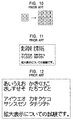
- Fig. 10 shows the conventional horizontal/vertical doubling conversion method.
- data for four original pixels A, B, C, and D are horizontally and vertically doubled and converted into sixteen pixels
- each data of the original pixels A, B, C, and D is applied unchanged to four-pixel data obtained by the horizontal/vertical doubling conversion.
- four pixels are regarded as one pixel, and display is performed in this way.
- Fig. 11 shows an example of an image before the image is enlarged.
- Fig. 12 shows an example of the same image after the conventional doubling conversion is performed.
- the jaggies in the contours of characters are relatively unnoticeable.
- the jagged contours in curved portions of the characters become noticeable. It can be concluded that image quality is degraded by reduction in the density of displayed information.
- the pixel resolution converting circuit includes a data array pattern comparing unit for binarizing an input video signal.
- the data array pattern comparing unit compares a 3-by-3 (nine) pixel array pattern of input image data, including a pixel to be converted and eight pixels vertically, horizontally, and diagonally surrounding the pixel to be converted, and a specific array pattern selected from all possible array patterns formed by combinations of 3-by-3 (nine) pixel binary image data. As a result, it is determined whether the array pattern of the input image data matches the specific array pattern.
- an enlarged image data generating unit applies image data differing from that of the pixel to be converted to part of image data corresponding to four pixels obtained by vertically and horizontally doubling the pixel to be converted.
- the same image data as that of the pixel to be converted is applied to the image data corresponding to all four pixels.
- the image data information about the pixel to be converted and about the surrounding eight pixels is reflected in the image data of the four pixels obtained by enlargement of the pixel to be converted.
- the image data differing from that of the pixel to be converted is applied to part of the image data of the four pixels. Accordingly, the jagged portions in the contour in the diagonal direction can be minimized, thus preventing image quality from being degraded by enlargement.
- the specific array pattern includes an array pattern in which the image data of the pixel to be converted differs from one of image data of pixels above and below the pixel to be converted, and differs from one of image data of pixels at the left and the right of the pixel to be converted.
- the enlarged image data generating unit differentiate, among the image data of the four pixels to be generated, only image data corresponding to a position adjacent to both pixels having the different image data from the image data of the pixel to be converted.
- the pixel to be converted forms, for example, part of the contour in the diagonal direction.
- the pixel among the four pixels obtained by vertically and horizontally doubling the pixel to be converted, to which the image data differing from that of the pixel to be converted is to be applied. This minimizes the jagged portions in the contour in the diagonal direction, and thereby prevents image quality from being degraded by enlargement.
- the specific array pattern may include any one of an array pattern in which the number of pixels having the image data differing from that of the pixel to be converted is three, there being at least one pair of adjacent pixels having the different image data, an array pattern in which the number of pixels having the image data differing from that of the pixel to be converted is four, there being two or more pairs of adjacent pixels having the different image data, and an array pattern in which the number of pixels having the image data differing from that of the pixel to be converted is five, there being three or more pairs of adjacent pixels having the different image data.
- the enlarged image data generating unit differentiate, among the image data of the four pixels to be generated, only image data corresponding to a position adjacent to both pixels having the different image data from the image data of the pixel to be converted.
- the specific array pattern is a pattern in which, among the image data of the eight pixels surrounding the pixel to be converted, the number of pixels having image data differing from that of the pixel to be converted is three, there being two pairs of adjacent pixels having the different image data, and when the position of the pixel to be converted is in an even column and an even row or in an odd column and an odd row, it is preferable that the enlarged image data generating unit differentiate, among the image data of the four pixels to be generated, only image data corresponding to a position adjacent to both pixels having the different image data from the image data of the pixel to be converted.
- an image display device including the above-described pixel resolution converting circuit. According to the image display device, it is possible to perform enlarged display in which a displayed image is vertically and horizontally doubled without degrading image quality.
- Fig. 1 shows an example of the structure of an image display device according to an embodiment of the present invention.
- a pixel resolution converting circuit according to an embodiment of the present invention and surrounding portions for performing doubling enlargement processing are illustrated.
- Fig. 2 conceptually shows the enlargement processing of the present invention.
- a target pixel A at the center of input image data D is converted into four pixels A1 to A4 by referring to the eight pixels surrounding pixel A.
- an input video signal 1 is delayed for one line by a line memory group 2 so that reference to the surrounding eight pixels can be made.
- a resultant video signal 6 for three lines is input to a pixel resolution converting circuit 3.
- the pixel resolution converting circuit 3 refers to data of the target pixel and to data of the surrounding eight pixels, and converts one-pixel data into four-pixel data. Then, the pixel resolution converting circuit 3 converts the four-pixel data into a signal 4 for each line.
- a display unit 5 performs enlarged display of the input data.
- the conversion processing is described in detail. Subsequent to binarization of the data of the target pixel and the data of the surrounding eight pixels, the arrangement of the pixels is checked.
- the center of the dynamic range or the average of reference pixel data is employed as a threshold for performing binarization. Alternatively, the threshold can appropriately be changed in accordance with characteristics of the video signals.
- the binarized pixel data is referred to as "0" or "1". These two binary patterns indicate black by "0" and white by "1".
- the target pixel is 0 (black)
- the surrounding eight pixels can be in patterns shown in Fig. 4.
- the target pixel is 1 (white)
- possible data patterns of the surrounding eight pixels are shown in Fig. 5. Besides these patterns shown in Figs.
- Figs. 6 and 7 show conversion rules corresponding to the patterns encircled by dotted lines in Figs. 4 and 5, respectively.
- the target pixel is converted into four pixels as indicated by an arrow.
- Fig. 6 shows cases when the target pixel is 0 (black).
- Fig. 7 shows cases when the target pixel is 1 (white). More specifically, pattern 6a shown in Fig. 6 is such that the target pixel is 0 (black).
- Four pixels obtained by conversion are such that a lower left pixel is 1 (white), and the remaining three pixels are 0 (black). In this conversion, the data of the target pixel prior to binarization is applied unchanged to the black pixels.
- shaded pixels may be either 0 (black) or 1 (white).
- pattern 6a in Fig. 6 indicates the following.
- the image data (0, black) of the target pixel differs from one of the pixels (1, white) above and below the target pixel, and differs from one of the pixels (1, white) at the right and the left of the target pixel.
- image data of four generated pixels only image data corresponding to the position adjacent to the pixels (left-hand side and lower center) whose image data differ from that of the target pixel is made different (1, white) from the image data of the target pixel.
- Fig. 7 the values 0 (black) and 1 (white) in Fig. 6 are inverted. In this case, the same processing is performed as in Fig. 6. Among four pixels obtained by conversion, data of the target pixel before binarization is applied unchanged to pixels having 1 (white). To pixels having 0 (black), the average of pixel data indicated by circles among the eight surrounding pixels before binarization is applied. For 90°, 180°, and 270° rotated patterns of the patterns shown in Figs. 6 and 7, similar processing is performed
- pattern 6h in Fig. 6 and to pattern 7h in Fig. 7 (encircled by dotted lines) when converting the target pixel.
- pattern 6h and pattern 7h are alternately converted.
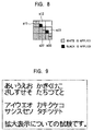
- a pattern shown in Fig. 8 is obtained.
- pattern 6h in Fig. 6 and pattern 7h in Fig. 7 are converted in the same manner despite the position of the target pixel, the following problem occurs. More specifically, when the target pixel is 0 (black) as in pattern 6h in Fig. 6, four pixels obtained by conversion are such that the upper right pixel becomes 1 (white).
- the target pixel is 1 (white), and, among four pixels obtained by conversion, the lower left pixel becomes 0 (black).
- the result of conversion is such as that shown in Fig. 8.
- 1 (white) is applied to each upper right pixel.
- 0 (black) is applied to each lower left pixel.
- pattern 6h in Fig. 6 and pattern 7h in Fig. 7 are converted only when each target pixel is in an even column and in an even row, or in an odd column and in an odd row.
- the groups a11, a22, and a33 of four pixels, each disposed in an even column and in an even row, or in an odd column and in an odd row, are converted such that 1 (white) is applied to each upper right pixel.
- each lower left pixel is not converted to 0 (black). All four pixels in each of the groups a12 and a23 become 1 (white).
- Fig. 9 shows an example of an image obtained by performing doubling enlargement by the present invention of the image shown in Fig. 11.
- the image shown in Fig. 9 is enlarged and displayed without being degraded in image quality by reduction in information.
- FIG. 3 the pixel resolution converting circuit 3 of the embodiment is illustrated. It is assumed that the processing is performed by a digital circuit. In Fig. 3, a clock signal and the like are omitted in order to avoid complexity.
- the video signal 6 for three lines is input to a binarization comparator 7 and to an averaging circuit 25.
- the binarization comparator 7 sequentially binarizes the input video signal 6. Subsequently, the binarization comparator 7 holds binary data (0, 1) of a target pixel and surrounding eight pixels, and outputs the data to a checking circuit A 8.
- a pattern holding circuit 9 holds binary patterns of 3-by-3 nine pixels, corresponding to those shown in Fig. 6, in the form of 0 and 1 values.
- the pattern holding circuit 9 is formed by a ROM or a RAM.
- the pattern holding circuit 9 outputs data corresponding to each pattern to the checking circuit A 8.
- the checking circuit A 8 checks correspondence between the pixel data output from the binarization comparator 7 and the data output from the pattern holding circuit 9.
- the checking circuit A 8 outputs a matching detection signal 11 to a matched flag register A 10 only when all nine pixels in each pattern in Fig. 6 are matched or unmatched. Detecting the pattern in which all nine pixels are unmatched is equivalent to performing matching detection for patterns in Fig. 7 in which black and white are inverted.
- the matching detection signal 11 includes information for discriminating a matched pattern from eight patterns in Fig. 6, and rotation information about the matched pattern. This rotation information is employed to discriminate a pattern as one of 0°, 90°, 180°, and 270° rotations of each pattern.
- the pattern output from the binarization comparator 7 to the checking circuit A 8 corresponds to the positional information of the video signal 6 for three lines.
- the rotation information indicates that the pattern is rotated 0°.
- the initial state of the matched flag register A 10 is set to a state in which matching is not detected.
- the matched flag register A 10 holds matching detection information only when such information is included in the matching detection signal 11 transmitted from the checking circuit A 8.
- the binarization comparator 7 transmits binary data of the target pixel and surrounding eight pixels to a 90° mapping circuit A 12.
- the 90° mapping circuit A 12 holds binary data of nine pixels in such a pattern that the surrounding eight pixels are rotated 90° around the central target pixel.
- the 90° mapping circuit A 12 outputs the binary data to a checking circuit B 13. Since the pattern holding circuit 9 outputs to the checking circuit B 13 the same data as that output to the checking circuit A 8, the checking circuit B 13 performs detection processing similar to that performed by the checking circuit A 8.
- a matching detection signal 14 includes information for discriminating a matched pattern and rotation information about the pattern which indicates that the pattern is rotated 90°.
- a matched flag register B 15 holds the matching detection signal 14.
- the 90° mapping circuit A 12, a 90° mapping circuit B 16, and a 90° mapping circuit C 20 perform matching detection of 90°, 180°, and 270° rotated patterns of the patterns shown in Fig. 6.
- the matched flag register A 10, the matched flag register B 15, a matched flag register C 19, and a matched flag register D 23 include components constructed by shift registers. These matched flag registers 10, 15, 19, and 23 sequentially hold matching detection information for each of 0°, 90°, 180°, and 270° rotations of the patterns in Fig. 6.
- the matched flag register D 23 outputs the initial state of the matched flag register A 10 as an output 24.
- the matching detection processing is performed by pipeline processing for each rotation of the patterns. Alternatively, if it is possible, the matching detection processing can be performed in batch processing.
- the averaging circuit 25 performs conversion processing shown in Figs. 6 and 7 based on the video signal 6 for three lines and the output 24 from the matched flag register D 23.
- the conversion processing is performed by determining, among four pixels obtained by conversion, pixels to which the data of the target pixel is to be applied unchanged, and pixels to which the average of pixels indicated by circles is to be applied. As a result, data of the four converted pixels are obtained.
- the conversion processing is performed by a arithmetic logical circuit. When pattern 6h in Fig. 6 and pattern 7h in Fig. 7 are converted, a synchronization signal 29 and a clock are counted, thus determining the position of the pixel, that is, determining whether the pixel is in an even column and in an even row, etc. The conversion processing is thereby performed.
- the averaging circuit 25 outputs data 28 of the four converted pixels. Since the data 28 is pixel data for two lines, it is necessary to take into consideration an interface with a general video signal. Hence, a line memory group 26 and a multiplexer (MUX) 27 are employed to convert the data 28 into one-line sequential image data, and output a signal 4 for each line.
- MUX multiplexer
Landscapes
- Physics & Mathematics (AREA)
- General Physics & Mathematics (AREA)
- Engineering & Computer Science (AREA)
- Theoretical Computer Science (AREA)
- Control Of Indicators Other Than Cathode Ray Tubes (AREA)
- Image Processing (AREA)
- Studio Circuits (AREA)
- Controls And Circuits For Display Device (AREA)
- Editing Of Facsimile Originals (AREA)
Abstract
Description
Claims (8)
- A pixel resolution converting circuit for doubling and outputting a horizontal pixel resolution and a vertical pixel resolution of an input image signal, said pixel resolution converting circuit comprising:data array pattern comparing means for binarizing the input video signal, for comparing a 3-by-3 (nine) pixel array pattern of input image data, including a pixel to be converted and eight pixels vertically, horizontally, and diagonally surrounding the pixel to be converted, and a specific array pattern selected from all possible array patterns formed by combinations of 3-by-3 (nine) pixel binary image data, and for determining whether the array pattern of the input image data matches the specific array pattern; andenlarged image data generating means for applying, when the array pattern of the input image data matches the specific array pattern, image data differing from that of the pixel to be converted to part of image data corresponding to four pixels obtained by vertically and horizontally doubling the pixel to be converted, and, when the array pattern of the input image data does not match the specific array pattern, for applying the same image data as that of the pixel to be converted to the image data corresponding to all four pixels.
- A pixel resolution converting circuit according to Claim 1, wherein, when the specific array pattern includes an array pattern in which the image data of the pixel to be converted differs from one of image data of pixels above and below the pixel to be converted, and differs from one of image data of pixels at the left and the right of the pixel to be converted, said enlarged image data generating means differentiates, among the image data of the four pixels to be generated, only image data corresponding to a position adjacent to both pixels having the different image data from the image data of the pixel to be converted.
- A pixel resolution converting circuit according to Claim 2, wherein, among the image data of the eight pixels surrounding the pixel to be converted, when the specific array pattern includes any one of an array pattern in which the number of pixels having the image data differing from that of the pixel to be converted is three, there being at least one pair of adjacent pixels having the different image data, an array pattern in which the number of pixels having the image data differing from that of the pixel to be converted is four, there being two or more pairs of adjacent pixels having the different image data, and an array pattern in which the number of pixels having the image data differing from that of the pixel to be converted is five, there being three or more pairs of adjacent pixels having the different image data, said enlarged image data generating means differentiates, among the image data of the four pixels to be generated, only image data corresponding to a position adjacent to both pixels having the different image data from the image data of the pixel to be converted.
- A pixel resolution converting circuit according to Claim 3, wherein, when the specific array pattern is a pattern in which, among the image data of the eight pixels surrounding the pixel to be converted, the number of pixels having image data differing from that of the pixel to be converted is three, there being two pairs of adjacent pixels having the different image data, and when the position of the pixel to be converted is in an even column and an even row or in an odd column and an odd row, said enlarged image data generating means differentiates, among the image data of the four pixels to be generated, only image data corresponding to a position adjacent to both pixels having the different image data from the image data of the pixel to be converted.
- An image display device comprising a pixel resolution converting circuit as set forth in Claim 1.
- An image display device according to Claim 5, wherein, in said pixel resolution converting circuit, when the specific array pattern includes an array pattern in which the image data of the pixel to be converted differs from one of image data of pixels above and below the pixel to be converted, and differs from one of image data of pixels at the left and the right of the pixel to be converted, said enlarged image data generating means differentiates, among the image data of the four pixels to be generated, only image data corresponding to a position adjacent to both pixels having the different image data from the image data of the pixel to be converted.
- An image display device according to Claim 6, wherein, in said pixel resolution converting circuit, among the image data of the eight pixels surrounding the pixel to be converted, when the specific array pattern includes any one of an array pattern in which the number of pixels having the image data differing from that of the pixel to be converted is three, there being at least one pair of adjacent pixels having the different image data, an array pattern in which the number of pixels having the image data differing from that of the pixel to be converted is four, there being two or more pairs of adjacent pixels having the different image data, and an array pattern in which the number of pixels having the image data differing from that of the pixel to be converted is five, there being three or more pairs of adjacent pixels having the different image data, said enlarged image data generating means differentiates, among the image data of the four pixels to be generated, only image data corresponding to a position adjacent to both pixels having the different image data from the image data of the pixel to be converted.
- An image display device according to Claim 7, wherein, in said pixel resolution converting circuit, when the specific array pattern is a pattern in which, among the image data of the eight pixels surrounding the pixel to be converted, the number of pixels having image data differing from that of the pixel to be converted is three, there being two pairs of adjacent pixels having the different image data, and when the position of the pixel to be converted is in an even column and an even row or in an odd column and an odd row, said enlarged image data generating means differentiates, among the image data of the four pixels to be generated, only image data corresponding to a position adjacent to both pixels having the different image data from the image data of the pixel to be converted.
Applications Claiming Priority (2)
| Application Number | Priority Date | Filing Date | Title |
|---|---|---|---|
| JP19372199 | 1999-07-07 | ||
| JP19372199A JP3676948B2 (en) | 1999-07-07 | 1999-07-07 | Pixel number conversion circuit and image display apparatus using the same |
Publications (2)
| Publication Number | Publication Date |
|---|---|
| EP1067477A2 true EP1067477A2 (en) | 2001-01-10 |
| EP1067477A3 EP1067477A3 (en) | 2004-04-14 |
Family
ID=16312700
Family Applications (1)
| Application Number | Title | Priority Date | Filing Date |
|---|---|---|---|
| EP00304890A Withdrawn EP1067477A3 (en) | 1999-07-07 | 2000-06-09 | Pixel resolution converting circuit and image display using the same |
Country Status (5)
| Country | Link |
|---|---|
| US (1) | US6624825B1 (en) |
| EP (1) | EP1067477A3 (en) |
| JP (1) | JP3676948B2 (en) |
| KR (1) | KR100367900B1 (en) |
| TW (1) | TW521260B (en) |
Families Citing this family (11)
| Publication number | Priority date | Publication date | Assignee | Title |
|---|---|---|---|---|
| JP3604993B2 (en) * | 2000-03-16 | 2004-12-22 | シャープ株式会社 | Image encoding device, image encoding method, image decoding device, and image decoding method |
| JP4617730B2 (en) * | 2004-06-15 | 2011-01-26 | ソニー株式会社 | Image processing apparatus and method, recording medium, and program |
| US7242412B2 (en) * | 2005-02-09 | 2007-07-10 | Seiko Epson Corporation | Method and apparatus for expanding a source pixel in a digital image |
| US8866707B2 (en) * | 2005-03-31 | 2014-10-21 | Semiconductor Energy Laboratory Co., Ltd. | Display device, and apparatus using the display device having a polygonal pixel electrode |
| US7545385B2 (en) * | 2005-12-22 | 2009-06-09 | Samsung Electronics Co., Ltd. | Increased color depth, dynamic range and temporal response on electronic displays |
| US20070153024A1 (en) * | 2005-12-29 | 2007-07-05 | Samsung Electronics Co., Ltd. | Multi-mode pixelated displays |
| KR20070099170A (en) * | 2006-04-03 | 2007-10-09 | 엘지.필립스 엘시디 주식회사 | Data converting device and converting method and driving device and driving method of image display device using same |
| JP4650500B2 (en) * | 2008-02-25 | 2011-03-16 | コニカミノルタビジネステクノロジーズ株式会社 | Image processing apparatus and image processing method |
| US8289415B2 (en) | 2008-02-26 | 2012-10-16 | Nec Corporation | Blink signal detection circuit, blink signal detection method, object sensing apparatus, object sensing method, and imaging system |
| JP4506854B2 (en) * | 2008-03-04 | 2010-07-21 | 富士ゼロックス株式会社 | Image processing apparatus and image forming apparatus |
| KR101466985B1 (en) * | 2008-04-03 | 2014-12-02 | 엘지디스플레이 주식회사 | Display device |
Family Cites Families (14)
| Publication number | Priority date | Publication date | Assignee | Title |
|---|---|---|---|---|
| US4437122A (en) * | 1981-09-12 | 1984-03-13 | Xerox Corporation | Low resolution raster images |
| US5170442A (en) * | 1987-09-08 | 1992-12-08 | Seiko Epson Corporation | Character pattern transforming system |
| CA1335794C (en) * | 1988-04-07 | 1995-06-06 | Yoshiyuki Okada | Process and apparatus for image magnification |
| EP0496600B1 (en) * | 1991-01-25 | 1997-01-02 | Canon Kabushiki Kaisha | Image processing apparatus |
| JP3478861B2 (en) * | 1994-02-01 | 2003-12-15 | 株式会社リコー | Smoothing enlargement processing method for binary image data |
| JPH07281637A (en) | 1994-04-11 | 1995-10-27 | Hitachi Ltd | Liquid crystal display, multi-resolution display method |
| JPH0879516A (en) * | 1994-09-01 | 1996-03-22 | Fuji Xerox Co Ltd | Image processor |
| JPH08227456A (en) * | 1994-09-22 | 1996-09-03 | Casio Comput Co Ltd | Dot pattern smoothing device and method |
| US5757982A (en) * | 1994-10-18 | 1998-05-26 | Hewlett-Packard Company | Quadrantal scaling of dot matrix data |
| MY117289A (en) | 1996-01-17 | 2004-06-30 | Sharp Kk | Image data interpolating apparatus |
| US6151025A (en) * | 1997-05-07 | 2000-11-21 | Hewlett-Packard Company | Method and apparatus for complexity reduction on two-dimensional convolutions for image processing |
| US6002813A (en) * | 1997-07-10 | 1999-12-14 | Samsung Electronics Co., Ltd. | Interpolation method for binary image |
| JP4050822B2 (en) * | 1998-05-14 | 2008-02-20 | パナソニック コミュニケーションズ株式会社 | Image scaling processing apparatus and image scaling processing method |
| US6430321B1 (en) * | 1998-09-28 | 2002-08-06 | Hewlett-Packard Company | Text enhancement |
-
1999
- 1999-07-07 JP JP19372199A patent/JP3676948B2/en not_active Expired - Fee Related
-
2000
- 2000-06-09 EP EP00304890A patent/EP1067477A3/en not_active Withdrawn
- 2000-06-20 TW TW089112115A patent/TW521260B/en not_active IP Right Cessation
- 2000-06-29 KR KR10-2000-0036351A patent/KR100367900B1/en not_active Expired - Fee Related
- 2000-07-06 US US09/611,435 patent/US6624825B1/en not_active Expired - Lifetime
Also Published As
| Publication number | Publication date |
|---|---|
| KR100367900B1 (en) | 2003-01-14 |
| US6624825B1 (en) | 2003-09-23 |
| JP3676948B2 (en) | 2005-07-27 |
| KR20010021037A (en) | 2001-03-15 |
| TW521260B (en) | 2003-02-21 |
| EP1067477A3 (en) | 2004-04-14 |
| JP2001022342A (en) | 2001-01-26 |
Similar Documents
| Publication | Publication Date | Title |
|---|---|---|
| US6389163B1 (en) | Method and apparatus for automatic image segmentation using template matching filters | |
| US4510618A (en) | Noise cleaner for binary images | |
| US6377711B1 (en) | Methods and systems for detecting the edges of objects in raster images using diagonal edge detection | |
| US6624825B1 (en) | Pixel resolution converting circuit and image display device using the same | |
| JP2967014B2 (en) | Image processing device | |
| JP3716527B2 (en) | 2D code reading method | |
| US5680485A (en) | Method and apparatus employing erosion-based filter pairs for image mapping | |
| JP3215768B2 (en) | Image processing device | |
| US5687252A (en) | Image processing apparatus | |
| US6795592B2 (en) | Architecture for processing fingerprint images | |
| JP2874592B2 (en) | Image processing device for distinguishing text / photo / dot area | |
| JPH0793563A (en) | Image processing device | |
| US7079699B2 (en) | Multi-valued image conversion device, multi-valued image conversion program, and multi-valued image conversion method | |
| JPH06150059A (en) | Image area separator | |
| US8116572B2 (en) | Method for detecting image edge and image interpolation using the same | |
| JPH0490082A (en) | Device for detecting character direction in document | |
| JP4519272B2 (en) | Pattern inspection apparatus and pattern inspection method | |
| JPH07182503A (en) | Image processing method and apparatus | |
| JPH02105272A (en) | Picture processor | |
| JP3320124B2 (en) | Image reading device | |
| JPH0129643Y2 (en) | ||
| JPH0211948B2 (en) | ||
| JPH01276971A (en) | Picture processor | |
| JPH04369173A (en) | Document reader | |
| JPS59135573A (en) | Identifying system of photo region |
Legal Events
| Date | Code | Title | Description |
|---|---|---|---|
| PUAI | Public reference made under article 153(3) epc to a published international application that has entered the european phase |
Free format text: ORIGINAL CODE: 0009012 |
|
| AK | Designated contracting states |
Kind code of ref document: A2 Designated state(s): AT BE CH CY DE DK ES FI FR GB GR IE IT LI LU MC NL PT SE |
|
| AX | Request for extension of the european patent |
Free format text: AL;LT;LV;MK;RO;SI |
|
| PUAL | Search report despatched |
Free format text: ORIGINAL CODE: 0009013 |
|
| AK | Designated contracting states |
Kind code of ref document: A3 Designated state(s): AT BE CH CY DE DK ES FI FR GB GR IE IT LI LU MC NL PT SE |
|
| AX | Request for extension of the european patent |
Extension state: AL LT LV MK RO SI |
|
| 17P | Request for examination filed |
Effective date: 20040423 |
|
| AKX | Designation fees paid |
Designated state(s): DE FR GB NL |
|
| 17Q | First examination report despatched |
Effective date: 20070612 |
|
| STAA | Information on the status of an ep patent application or granted ep patent |
Free format text: STATUS: THE APPLICATION IS DEEMED TO BE WITHDRAWN |
|
| 18D | Application deemed to be withdrawn |
Effective date: 20110104 |