EP1067454A1 - Touch panel - Google Patents
Touch panel Download PDFInfo
- Publication number
- EP1067454A1 EP1067454A1 EP00900338A EP00900338A EP1067454A1 EP 1067454 A1 EP1067454 A1 EP 1067454A1 EP 00900338 A EP00900338 A EP 00900338A EP 00900338 A EP00900338 A EP 00900338A EP 1067454 A1 EP1067454 A1 EP 1067454A1
- Authority
- EP
- European Patent Office
- Prior art keywords
- transparent
- electrode sheet
- touch panel
- film
- lower electrode
- Prior art date
- Legal status (The legal status is an assumption and is not a legal conclusion. Google has not performed a legal analysis and makes no representation as to the accuracy of the status listed.)
- Withdrawn
Links
Images

Classifications
-
- G—PHYSICS
- G06—COMPUTING OR CALCULATING; COUNTING
- G06F—ELECTRIC DIGITAL DATA PROCESSING
- G06F3/00—Input arrangements for transferring data to be processed into a form capable of being handled by the computer; Output arrangements for transferring data from processing unit to output unit, e.g. interface arrangements
- G06F3/01—Input arrangements or combined input and output arrangements for interaction between user and computer
- G06F3/03—Arrangements for converting the position or the displacement of a member into a coded form
- G06F3/041—Digitisers, e.g. for touch screens or touch pads, characterised by the transducing means
-
- G—PHYSICS
- G06—COMPUTING OR CALCULATING; COUNTING
- G06F—ELECTRIC DIGITAL DATA PROCESSING
- G06F3/00—Input arrangements for transferring data to be processed into a form capable of being handled by the computer; Output arrangements for transferring data from processing unit to output unit, e.g. interface arrangements
- G06F3/01—Input arrangements or combined input and output arrangements for interaction between user and computer
- G06F3/03—Arrangements for converting the position or the displacement of a member into a coded form
- G06F3/041—Digitisers, e.g. for touch screens or touch pads, characterised by the transducing means
- G06F3/045—Digitisers, e.g. for touch screens or touch pads, characterised by the transducing means using resistive elements, e.g. a single continuous surface or two parallel surfaces put in contact
Definitions
- the present invention relates to a touch panel placed on a screen of display devices such as LCDs (liquid crystal displays), CRTs (cathode ray tubes), or the like with which position input is obtained by being depressed from above by a finger or pen in accordance with instructions on the seen-through screen.
- LCDs liquid crystal displays
- CRTs cathode ray tubes
- a transparent touch panel of a resistance film system is so constructed that a pair of an upper electrode sheet 101 and a lower electrode sheet 102 having transparent electrodes of ITO or the like on transparent films respectively are arranged opposite to each other via spacers 103 of an insulating substance between the electrodes, and a transparent hold plate 105 of a resin totally is bonded to a lower face of the lower electrode sheet 102 via a transparent adhesive layer 104 (referring to Fig. 5).
- a polyethylene terephthalate film of a thickness of 100-200 ⁇ m superior in flexibility to pressing at the input time is used, which is generally biaxially stretched.
- a polycarbonate plate of a thickness of 0.5-3.0mm with a superior rigidity for protecting a screen of an LCD or the like from pressing at the input time is used, which is generally unstretched.
- the polyethylene terephthalate film used for the transparent film of the lower electrode sheet 102 and the polycarbonate plate used for the transparent hold plate 105 are different in thermal expansion coefficient, and moreover the former is stretched whereas the latter is unstretched.
- the transparent film of the lower electrode sheet 102 is bonded totally, that is, over the entire face to the transparent hold plate 105.
- the transparent hold plate 105 changes differently in size between the side of the lower electrode sheet and the opposite side when the touch panel is exposed to a severe temperature environment or humidity environment.
- the touch panel sometimes warps to project upward at its central part (with reference to Fig. 5). This warp produces an air layer between the touch panel and the screen under the touch panel, whereby a sense of touch in operation is dulled because of an unnecessary deflection applied to the whole of the touch panel at the input time.
- the warp could be forcibly corrected to make the touch panel flat in setting the touch panel on the screen of the LCD, CRT, or the like.
- This leads to waving the transparent film of the upper electrode sheet 101 and worsening an appearance or look of the touch panel and a visibility of the screen.
- the waving of the transparent film of the upper electrode sheet 101 changes a gap between electrodes irregularly, consequently varying the sense of touch depending on spots of the touch panel. An insulation failure may also be brought about through mutual touch of the electrodes if the waving of a large size takes place.
- An object of the present invention is therefore to provide a touch panel superior in flexibility for a pressing operation at the input time and rigidity for protecting a screen of a display device such as an LCD, CRT, or the like from the pressing operation, which hardly warps even exposed to a severe temperature environment or humidity environment, with solving the above-described issues.
- the present invention is so constructed as follows.
- a touch panel in which an upper electrode sheet having an upper transparent electrode formed on a transparent film of polyethylene terephthalate and a lower electrode sheet having a lower transparent electrode formed on a transparent film of polycarbonate are arranged opposite to each other via a plurality of spacers of an insulating substance between the upper and lower electrodes, while a transparent hold plate of a polycarbonate plate is bonded over an entire face to a lower face of the lower electrode sheet via a transparent adhesion layer.
- the touch panel according to the first aspect which uses a polycarbonate film of a thickness of 50-300 ⁇ m for the transparent film of the lower electrode sheet.
- the touch panel according to the first or second aspect is a polycarbonate plate of a thickness of 0.5-3.0mm having a rigidity for protecting a screen of a display apparatus from pressing at the input time.
- the touch panel according to any one of the first through third aspects in which the transparent adhesion layer is a transparent acrylic adhesive approximate in refractive index to the transparent film of the lower electrode sheet and the transparent hold plate.
- the touch panel in any one of the first through fourth aspects which uses a polycarbonate film of a thickness of 50-300 ⁇ m for the film of the lower electrode sheet, with the transparent adhesion layer being adapted to keep an elastic modulus of 5 ⁇ 10 5 -5 ⁇ 10 7 dynes/cm 2 at ordinary temperatures.
- the touch panel according to any one of the first through fifth aspects which is arranged on a screen of a display apparatus to enable position input when pressed from above by a finger or pen in accordance with instructions on the seen-through screen.
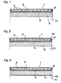
- Fig. 1 shows the basic constitution of a touch panel according to one embodiment of the present invention.
- An upper electrode sheet 1 with an upper transparent electrode is arranged on a transparent film, while a lower electrode sheet 2 with a lower transparent electrode is arranged on a different transparent film.
- the electrode sheets 1, 2 are set to be opposite to each other via a plurality of spacers 3 of an insulating substance between the upper and lower electrodes.
- a transparent hold plate 5 of a resin is wholly bonded to a lower face of the lower electrode sheet 2 via a transparent adhesion layer 4.
- a polyethylene terephthalate film is used for the transparent film of the upper electrode sheet 1, which has a thickness of 100-200 ⁇ m with a superior flexibility for pressing operation at an input time.
- a hard coat layer 70 of a thermosetting type resin such as an acryl epoxy resin or an urethane resin, a photosetting type resin such as an acrylate resin, or the like may be set to a face of the upper electrode sheet 1 opposite to the face where the upper transparent electrode thereof is provided.
- the transparent film of the upper electrode sheet 1 is obtained by continuously forming the upper transparent electrodes to a roll of film material and then cutting to a size of the upper electrode sheet 1.
- the transparent film of the lower electrode sheet 2 is used a polycarbonate film of a thickness of 50-300 ⁇ m to be different in material from the transparent film of the upper electrode sheet 1.
- the transparent film of the lower electrode sheet 2 is of the equal material to the transparent hold plate 5. Therefore, even in the case where the touch panel is exposed to severe temperature and humidity environments, for instance, at a high temperature of 70°C, at a low temperature of -20°C, at a high temperature and a high humidity of 60°C and 90%R/H, or the like, the transparent hold plate 5 hardly differs in size change between the side of the lower electrode sheet 2 and the opposite side, thus almost eliminating a warp from the touch panel.
- the polycarbonate film has a higher transmittance than the polyethylene terephthalate film of an equal thickness, thus improving a visibility of the touch panel in comparison with the case where the polyethylene terephthalate film is used for the transparent film of the lower electrode sheet 2.
- the transparent film of the lower electrode sheet 2 is obtained by continuously forming the transparent electrodes to a roll of film material and then cutting to a size of the lower electrode sheet 2. A thickness of the transparent film of the lower electrode sheet 2 is consequently limited to the above range.
- Each transparent electrode set to opposing faces of the upper electrode sheet 1 and the lower electrode sheet 2 is formed by vacuum vapor deposition, sputtering, ion plating or the like to a metallic film or metallic oxide film with transparency and conductivity.
- the metallic oxide film of ITO, tin oxide, indium oxide, antimony oxide, zinc oxide, cadmium oxide, or the like; a composite film essentially consisting of these metallic oxides; or the metallic film of gold, silver, copper, tin, nickel, aluminum, palladium or the like can be used.
- a thickness of each transparent electrode is generally 100-1000 ⁇ .
- the spacer 3 is formed in an optional shape onto a surface of the transparent electrode of either the upper electrode sheet 1 or the lower electrode sheet 2.
- a photoprocess with use of an acrylate resin such as melamine acrylate resin, urethane acrylate resin, epoxy acrylate resin, methacryl acrylate resin, acryl acrylate resin, or the like; or a transparent photosetting type resin such as polyvinyl alcohol resin or the like is employed as a way of forming the spacers 3.
- the spacers 3 can be formed also by a printing method with use of an urethane-based transparent resin. In general, the spacers 3 are formed like dots each having a diameter of 30-100 ⁇ m and a height of 1-15 ⁇ m and arranged with a constant interval of 0.1-10mm.
- a polycarbonate plate of a thickness of 0.5-3.0mm which has a superior rigidity for protecting a screen of a display apparatus 71 (The display apparatus 71 is indicated by chain lines in Fig. 1 and by solid lines in Fig. 2) such as an LCD or the like from being pressed at the input time. If the thickness is smaller than 0.5mm, the plate cannot function as the hold plate 5. If the thickness exceeds 3.0mm, the plate is too thick and too heavy to place on the screen, resulting in an impractical touch panel.
- a low reflection treatment layer 72 subjected to a low reflection treatment may be provided to a lower face of the transparent hold plate 5 .
- a low reflection treatment layer 72 a low reflection material using a low refractive index resin such as a fluororesin, a silicon resin or the like is applied, a multilayer film of metal is formed, or the like treatment is carried out.
- the treatment may be executed to the lower face of the transparent hold plate 5 directly.
- the presence of the low reflection treatment layer 72 restricts reflection at the lower face of the transparent hold plate, with improving the transmittance (visibility) of the touch panel.
- the lower electrode sheet 2 and the transparent hold plate 5 are bonded at entire faces via the transparent adhesion layer 4.
- no air layer is present between the lower electrode sheet 2 and the transparent hold plate 5, so that an extra deflection to the upper electrode sheet 1 at the input time is prevented and a sense of touch and operation is prevented from being dull, with no attenuation of light at a boundary to the air layer.
- a transparent adhesive such as an acrylic adhesive can be used which is generally used to totally bond the lower electrode sheet 2 and the transparent hold plate 5.
- the transparent adhesion layer 4 one that has a refractive index approximate to that of the transparent film of the lower electrode sheet 2 and the transparent hold plate 5 is more preferred, and also one that has an elastic modulus of 5 ⁇ 10 5 -5 ⁇ 10 7 dynes/cm 2 at ordinary temperatures is preferred.
- the transparent adhesion layer 4 is thus adapted to keep an elastic modulus in a range of 5 ⁇ 10 5 -5 ⁇ 10 7 dynes/cm 2 at ordinary temperatures, the touch panel is almost prevented from warping and consequently the upper transparent electrode of the touch panel can be improved in durability against sliding. The durability against sliding is vital to the touch panel.
- the adhesive may be directly applied to the lower electrode sheet 2 or the transparent hold plate 5.
- a double-faced adhesive film with an adhesive applied to both faces of a thin transparent supporting film may be formed beforehand and bonded to the lower electrode sheet 2 or the transparent hold plate 5 to form the transparent adhesion layer 4.
- a double-faced tape without an adhesive or a base (supporting film) is preferable as the transparent adhesion layer 4.
- the presence of the supporting film does not impair the warp prevention function because the transparent adhesion layer 4 is held between the polycarbonate sheet of the lower electrode sheet 2 and the polycarbonate plate of the transparent hold plate 5.
- a transparent electrode of ITO or the like is set in a thickness of 200 ⁇ by sputtering to one face of a roll of polyethylene terephthalate film of a thickness of 200 ⁇ m. The film is then cut to a rectangle of a length of 89mm and a breadth of 68mm, whereby an upper electrode sheet is formed.
- a transparent electrode of ITO or the like is formed in a thickness of 200 ⁇ by sputtering to one face of a 100 ⁇ m-thick polycarbonate film of a roll. Then, the film is cut to a rectangle of a length of 89mm and a breadth of 68mm to form a lower electrode sheet.
- a urethane-based transparent resin is printed in dots on the transparent electrode of the lower electrode sheet, whereby spacers each having a diameter 50 ⁇ m and a height of 10 ⁇ m are arranged with an interval of 1mm.
- the upper electrode sheet and the lower electrode sheet are bonded by an acrylic adhesive (elastic modulus of 8 ⁇ 10 5 dynes/cm 2 ) of a thickness of 20 ⁇ m and a breadth of 5mm outside an area of a display face.
- an acrylic adhesive elastic modulus of 8 ⁇ 10 5 dynes/cm 2
- a low reflection material using a silicon-based resin is applied to one face of a transparent hold plate of a polycarbonate plate of a length 89mm, a breadth 68mm, and a thickness 1mm, that is, a low reflection treatment is executed to form a low reflection treatment layer.
- a transparent adhesion layer of an acrylic adhesive is applied and formed to a face of the transparent hold plate opposite to the face having the low reflection treatment layer, and bonded totally to a lower face of the lower electrode sheet.
- a touch panel is obtained in this manner.
- the touch panel is left for 240 hours under an environment of a temperature 60°C and a humidity 90%RH, and further left for 24 hours at a room temperature. A warp is measured thereafter. No warp is brought about to the touch panel.
- a comparison example uses a 200 ⁇ m-thick polyethylene terephthalate film for a transparent film of a lower electrode sheet, which is subjected to an environmental test similar to the working example.
- a central part of the touch panel warps to project up by 1.2mm.
- a character slide test is conducted to the working example.
- the characters of the Japanese katakana syllabary are input with a load 250gf by a polyacetal pen having a leading end of a radius 0.8R.
- a contact resistance (ON resistance) is measured after 200000 characters are sliding-input. Since the arrangement having the lower electrode sheet, the transparent adhesive layer, and the transparent hold plate has a buffer effect, the contact resistance does not increase even after the input, specifically, 0.5k ⁇ before the input and 0.5k ⁇ after the input. An improvement in slide durability of the upper transparent electrode is detected.
- a character slide test similar to the working example is carried out to another comparison example which uses the lower electrode sheet, the transparent adhesive layer, and a 1.1mm-thick soda-lime glass plate in place of the transparent hold plate.
- a contact resistance increases from 1.0k ⁇ before the input up to 2.0k ⁇ after the input.
- the upper transparent electrode is deteriorated.
- the touch panel according to the present invention in the constitution and operation as above exerts effects to be described below.
- the transparent hold plate since the polycarbonate film which is the same material as a plate material for the transparent hold plate is used for the transparent film of the lower electrode sheet, the transparent hold plate hardly generates a difference in size change between the side of the lower electrode sheet and the opposite side even when the touch panel is exposed to a severe temperature environment or humidity environment, and thus, the touch panel hardly warps.
- the transparent film of the lower electrode sheet can be obtained by forming transparent electrodes continuously to the rolled film material and then cutting to a size of the lower electrode sheet.
- the transparent hold plate is formed of a 0.5-3.0mm-thick polycarbonate sheet having a rigidity for protecting a screen of a display apparatus from pressing at the input time
- the touch panel is almost prevented from being deflected into touch with the display screen at the input time. If the touch panel were accidentally brought in touch with the display screen to cause the display apparatus to blur when the display apparatus is an LCD, the present invention can prevent such generation of blur.
- the transparent adhesion layer uses a transparent acrylic adhesive having a refractive index approximate to that of the transparent film of the lower electrode sheet and the transparent hold plate, the light is hardly reflected between the adhesion layer and the hold plate and between the lower electrode sheet and the adhesion layer, whereby the visibility is improved.
- the touch panel When a soft polycarbonate film of a thickness 50-300 ⁇ m is used for the film of the lower electrode sheet and the transparent adhesion layer is adapted to have an elastic modulus of 5 ⁇ 10 5 -5 ⁇ 10 7 dynes/cm 2 at ordinary temperatures, the touch panel hardly warps with the slide durability of the upper transparent electrode of the touch panel being improved. The slide durability is considerably important to the touch panel.
- the touch panel When the touch panel is arranged on a screen of a display apparatus to enable position input when pressed from above by a finger or pen in accordance with instructions on the see-through screen, the touch panel can be superior both in flexibility for pressing at the input time and in rigidity for protecting the screen of the display apparatus such as an LCD, a CRT, or the like from pressing at the input time. Also the touch panel hardly warps even when exposed to a severe temperature environment or humidity environment and is prevented from being worsened in appearance, thus preventing the screen from being decreased in visibility. A sense of input of the touch panel can be prevented from varying because of generation of the warp.
Landscapes
- Engineering & Computer Science (AREA)
- General Engineering & Computer Science (AREA)
- Theoretical Computer Science (AREA)
- Human Computer Interaction (AREA)
- Physics & Mathematics (AREA)
- General Physics & Mathematics (AREA)
- Position Input By Displaying (AREA)
- Laminated Bodies (AREA)
- Push-Button Switches (AREA)
Abstract
Description
With respective electrode faces set opposite to each other, the upper electrode sheet and the lower electrode sheet are bonded by an acrylic adhesive (elastic modulus of 8×10⁵dynes/cm2) of a thickness of 20µm and a breadth of 5mm outside an area of a display face.
Claims (6)
- A touch panel in which an upper electrode sheet (1) having an upper transparent electrode formed on a transparent film of polyethylene terephthalate and a lower electrode sheet (2) having a lower transparent electrode formed on a transparent film of polycarbonate are arranged opposite to each other via a plurality of spacers (3) of an insulating substance between the upper and lower electrodes, while a transparent hold plate (5) of a polycarbonate plate is bonded over an entire face to a lower face of the lower electrode sheet via a transparent adhesion layer (4).
- A touch panel according to claim 1, wherein a polycarbonate film of a thickness of 50-300µm is used for the transparent film of the lower electrode sheet (2).
- A touch panel according to claim 1 or 2, wherein the transparent hold plate (5) is the polycarbonate plate of a thickness of 0.5-3.0mm having a rigidity for protecting a screen of a display apparatus (71) from pressing at input time.
- A touch panel according to any one of claims 1-3, wherein the transparent adhesion layer (4) is a transparent acrylic adhesive approximate in refractive index to the transparent film of the lower electrode sheet (2) and the transparent hold plate (5).
- A touch panel according to any one of claims 1-4, wherein a polycarbonate film of a thickness of 50-300µm is used for the film of the lower electrode sheet, with the transparent adhesion layer being adapted to keep an elastic modulus of 5×10⁵-5×10⁷dynes/cm2 at ordinary temperatures.
- A touch panel according to any one of claims 1-5, which is arranged on a screen of the display apparatus (71) to enable position input when pressed from above by a finger or pen in accordance with instructions on the seen-through screen.
Applications Claiming Priority (3)
| Application Number | Priority Date | Filing Date | Title |
|---|---|---|---|
| JP514299 | 1999-01-12 | ||
| JP514299A JP3946371B2 (en) | 1999-01-12 | 1999-01-12 | Touch panel |
| PCT/JP2000/000097 WO2000042496A1 (en) | 1999-01-12 | 2000-01-12 | Touch panel |
Publications (2)
| Publication Number | Publication Date |
|---|---|
| EP1067454A1 true EP1067454A1 (en) | 2001-01-10 |
| EP1067454A4 EP1067454A4 (en) | 2006-08-02 |
Family
ID=11603065
Family Applications (1)
| Application Number | Title | Priority Date | Filing Date |
|---|---|---|---|
| EP00900338A Withdrawn EP1067454A4 (en) | 1999-01-12 | 2000-01-12 | Touch panel |
Country Status (6)
| Country | Link |
|---|---|
| US (1) | US6559902B1 (en) |
| EP (1) | EP1067454A4 (en) |
| JP (1) | JP3946371B2 (en) |
| KR (1) | KR100716738B1 (en) |
| TW (1) | TW446976B (en) |
| WO (1) | WO2000042496A1 (en) |
Cited By (3)
| Publication number | Priority date | Publication date | Assignee | Title |
|---|---|---|---|---|
| WO2005107072A1 (en) * | 2004-04-29 | 2005-11-10 | Smart Technologies Inc. | Tensioned touch panel and method of making same |
| US7517567B2 (en) * | 2002-03-26 | 2009-04-14 | Panasonic Corporation | Transparent touch panel and a method of manufacturing the same |
| EP2096525A3 (en) * | 2008-02-29 | 2013-10-09 | LG Electronics Inc. | Portable terminal |
Families Citing this family (111)
| Publication number | Priority date | Publication date | Assignee | Title |
|---|---|---|---|---|
| US5910854A (en) | 1993-02-26 | 1999-06-08 | Donnelly Corporation | Electrochromic polymeric solid films, manufacturing electrochromic devices using such solid films, and processes for making such solid films and devices |
| US5668663A (en) | 1994-05-05 | 1997-09-16 | Donnelly Corporation | Electrochromic mirrors and devices |
| US6891563B2 (en) * | 1996-05-22 | 2005-05-10 | Donnelly Corporation | Vehicular vision system |
| US6172613B1 (en) | 1998-02-18 | 2001-01-09 | Donnelly Corporation | Rearview mirror assembly incorporating vehicle information display |
| US6326613B1 (en) | 1998-01-07 | 2001-12-04 | Donnelly Corporation | Vehicle interior mirror assembly adapted for containing a rain sensor |
| US8294975B2 (en) | 1997-08-25 | 2012-10-23 | Donnelly Corporation | Automotive rearview mirror assembly |
| US6124886A (en) | 1997-08-25 | 2000-09-26 | Donnelly Corporation | Modular rearview mirror assembly |
| US6445287B1 (en) * | 2000-02-28 | 2002-09-03 | Donnelly Corporation | Tire inflation assistance monitoring system |
| US6690268B2 (en) | 2000-03-02 | 2004-02-10 | Donnelly Corporation | Video mirror systems incorporating an accessory module |
| US8288711B2 (en) | 1998-01-07 | 2012-10-16 | Donnelly Corporation | Interior rearview mirror system with forwardly-viewing camera and a control |
| US6693517B2 (en) | 2000-04-21 | 2004-02-17 | Donnelly Corporation | Vehicle mirror assembly communicating wirelessly with vehicle accessories and occupants |
| US6329925B1 (en) | 1999-11-24 | 2001-12-11 | Donnelly Corporation | Rearview mirror assembly with added feature modular display |
| US6477464B2 (en) | 2000-03-09 | 2002-11-05 | Donnelly Corporation | Complete mirror-based global-positioning system (GPS) navigation solution |
| US7167796B2 (en) | 2000-03-09 | 2007-01-23 | Donnelly Corporation | Vehicle navigation system for use with a telematics system |
| US7370983B2 (en) | 2000-03-02 | 2008-05-13 | Donnelly Corporation | Interior mirror assembly with display |
| TW548580B (en) * | 2000-11-27 | 2003-08-21 | Toshiaki Ishiyama | Glass touch panel |
| JP2002202855A (en) * | 2000-12-28 | 2002-07-19 | Matsushita Electric Ind Co Ltd | Touch panel and electronic device using the same |
| JP2002287902A (en) * | 2001-01-17 | 2002-10-04 | Seiko Epson Corp | Touch panel and electronic equipment |
| EP1363810B1 (en) | 2001-01-23 | 2007-05-30 | Donnelly Corporation | Improved vehicular lighting system |
| US7255451B2 (en) * | 2002-09-20 | 2007-08-14 | Donnelly Corporation | Electro-optic mirror cell |
| US7581859B2 (en) | 2005-09-14 | 2009-09-01 | Donnelly Corp. | Display device for exterior rearview mirror |
| JP2002313121A (en) * | 2001-04-16 | 2002-10-25 | Nitto Denko Corp | Illumination device with touch panel and reflective liquid crystal display device |
| JP2003050674A (en) * | 2001-08-08 | 2003-02-21 | Nagano Fujitsu Component Kk | Touch panel and input device equipped with touch panel |
| TWI224276B (en) * | 2001-11-02 | 2004-11-21 | Matsushita Electric Industrial Co Ltd | Touch panel and method of manufacturing the same |
| JP3880418B2 (en) | 2002-02-21 | 2007-02-14 | 日東電工株式会社 | Method for sticking and fixing double-sided adhesive sheet and touch panel to display device |
| US6918674B2 (en) | 2002-05-03 | 2005-07-19 | Donnelly Corporation | Vehicle rearview mirror system |
| WO2003105099A1 (en) | 2002-06-06 | 2003-12-18 | Donnelly Corporation | Interior rearview mirror system with compass |
| US7329013B2 (en) | 2002-06-06 | 2008-02-12 | Donnelly Corporation | Interior rearview mirror system with compass |
| JP3726900B2 (en) * | 2002-06-24 | 2005-12-14 | セイコーエプソン株式会社 | Display device and electronic apparatus equipped with the same |
| CN100483189C (en) * | 2002-08-20 | 2009-04-29 | 三星电子株式会社 | liquid crystal display device |
| US7310177B2 (en) | 2002-09-20 | 2007-12-18 | Donnelly Corporation | Electro-optic reflective element assembly |
| AU2003278863A1 (en) | 2002-09-20 | 2004-04-08 | Donnelly Corporation | Mirror reflective element assembly |
| US7289037B2 (en) | 2003-05-19 | 2007-10-30 | Donnelly Corporation | Mirror assembly for vehicle |
| JP2005010986A (en) * | 2003-06-18 | 2005-01-13 | Matsushita Electric Ind Co Ltd | Touch panel and manufacturing method thereof |
| JP2005100333A (en) * | 2003-09-04 | 2005-04-14 | Alps Electric Co Ltd | Coordinate input device, and liquid crystal display device and electronic apparatus comprising the same |
| US7446924B2 (en) | 2003-10-02 | 2008-11-04 | Donnelly Corporation | Mirror reflective element assembly including electronic component |
| US7308341B2 (en) | 2003-10-14 | 2007-12-11 | Donnelly Corporation | Vehicle communication system |
| ATE517368T1 (en) | 2005-05-16 | 2011-08-15 | Donnelly Corp | VEHICLE MIRROR ARRANGEMENT WITH CHARACTER ON THE REFLECTIVE PART |
| EP1949666B1 (en) | 2005-11-01 | 2013-07-17 | Magna Mirrors of America, Inc. | Interior rearview mirror with display |
| JP5196973B2 (en) | 2007-11-27 | 2013-05-15 | 富士通コンポーネント株式会社 | Electronic equipment with panel-type input device |
| JP5297668B2 (en) * | 2008-03-19 | 2013-09-25 | 株式会社ジャパンディスプレイ | Liquid crystal display |
| US8154418B2 (en) | 2008-03-31 | 2012-04-10 | Magna Mirrors Of America, Inc. | Interior rearview mirror system |
| JP5095814B2 (en) * | 2008-08-25 | 2012-12-12 | 日本写真印刷株式会社 | Touch input device and electronic device |
| GB0818918D0 (en) * | 2008-10-15 | 2008-11-19 | Icera Inc | Boot algorithm |
| TWI406164B (en) * | 2009-05-21 | 2013-08-21 | Ite Tech Inc | Touch panel dector with slider structure |
| KR101070137B1 (en) * | 2009-08-21 | 2011-10-05 | 삼성전기주식회사 | Touch feedback panel, touch screen device and electronic device including the same |
| KR101191117B1 (en) * | 2009-09-28 | 2012-10-15 | 주식회사 엘지화학 | Touch panel |
| US9128545B2 (en) | 2010-05-14 | 2015-09-08 | Racing Optics, Inc. | Touch screen shield |
| US9274625B2 (en) | 2010-05-14 | 2016-03-01 | Racing Optics, Inc. | Touch screen shield |
| US20170031525A1 (en) | 2010-05-14 | 2017-02-02 | Racing Optics, Inc. | Touch screen shield |
| US8575949B2 (en) | 2010-08-25 | 2013-11-05 | Ford Global Technologies, Llc | Proximity sensor with enhanced activation |
| US8454181B2 (en) | 2010-08-25 | 2013-06-04 | Ford Global Technologies, Llc | Light bar proximity switch |
| KR101385844B1 (en) * | 2010-10-20 | 2014-04-21 | 주식회사 엘지화학 | Pressure-sensitive adhesive composition for touch panel |
| US8044942B1 (en) | 2011-01-18 | 2011-10-25 | Aevoe Inc. | Touch screen protector |
| US8629944B2 (en) * | 2011-05-03 | 2014-01-14 | Innovation & Infinity Global Corp. | Transparent conductive structure applied to a touch panel and method of making the same |
| US8491986B2 (en) * | 2011-05-25 | 2013-07-23 | Htc Corporation | Panel module and manufacturing method thereof |
| US8928336B2 (en) | 2011-06-09 | 2015-01-06 | Ford Global Technologies, Llc | Proximity switch having sensitivity control and method therefor |
| US8975903B2 (en) | 2011-06-09 | 2015-03-10 | Ford Global Technologies, Llc | Proximity switch having learned sensitivity and method therefor |
| JP6051477B2 (en) * | 2011-07-19 | 2016-12-27 | エルジー・ケム・リミテッド | Touch panel |
| KR101595146B1 (en) * | 2011-07-19 | 2016-02-17 | 주식회사 엘지화학 | Touch panel |
| JP6043951B2 (en) * | 2011-08-02 | 2016-12-14 | パナソニックIpマネジメント株式会社 | Touch panel |
| US10004286B2 (en) | 2011-08-08 | 2018-06-26 | Ford Global Technologies, Llc | Glove having conductive ink and method of interacting with proximity sensor |
| US9143126B2 (en) | 2011-09-22 | 2015-09-22 | Ford Global Technologies, Llc | Proximity switch having lockout control for controlling movable panel |
| US10112556B2 (en) | 2011-11-03 | 2018-10-30 | Ford Global Technologies, Llc | Proximity switch having wrong touch adaptive learning and method |
| US8994228B2 (en) | 2011-11-03 | 2015-03-31 | Ford Global Technologies, Llc | Proximity switch having wrong touch feedback |
| US8878438B2 (en) | 2011-11-04 | 2014-11-04 | Ford Global Technologies, Llc | Lamp and proximity switch assembly and method |
| US9831870B2 (en) | 2012-04-11 | 2017-11-28 | Ford Global Technologies, Llc | Proximity switch assembly and method of tuning same |
| US9568527B2 (en) | 2012-04-11 | 2017-02-14 | Ford Global Technologies, Llc | Proximity switch assembly and activation method having virtual button mode |
| US9520875B2 (en) | 2012-04-11 | 2016-12-13 | Ford Global Technologies, Llc | Pliable proximity switch assembly and activation method |
| US9184745B2 (en) | 2012-04-11 | 2015-11-10 | Ford Global Technologies, Llc | Proximity switch assembly and method of sensing user input based on signal rate of change |
| US8933708B2 (en) | 2012-04-11 | 2015-01-13 | Ford Global Technologies, Llc | Proximity switch assembly and activation method with exploration mode |
| US9197206B2 (en) | 2012-04-11 | 2015-11-24 | Ford Global Technologies, Llc | Proximity switch having differential contact surface |
| US9559688B2 (en) | 2012-04-11 | 2017-01-31 | Ford Global Technologies, Llc | Proximity switch assembly having pliable surface and depression |
| US9531379B2 (en) | 2012-04-11 | 2016-12-27 | Ford Global Technologies, Llc | Proximity switch assembly having groove between adjacent proximity sensors |
| US9219472B2 (en) | 2012-04-11 | 2015-12-22 | Ford Global Technologies, Llc | Proximity switch assembly and activation method using rate monitoring |
| US9065447B2 (en) | 2012-04-11 | 2015-06-23 | Ford Global Technologies, Llc | Proximity switch assembly and method having adaptive time delay |
| US9287864B2 (en) | 2012-04-11 | 2016-03-15 | Ford Global Technologies, Llc | Proximity switch assembly and calibration method therefor |
| US9944237B2 (en) | 2012-04-11 | 2018-04-17 | Ford Global Technologies, Llc | Proximity switch assembly with signal drift rejection and method |
| US9660644B2 (en) | 2012-04-11 | 2017-05-23 | Ford Global Technologies, Llc | Proximity switch assembly and activation method |
| US9136840B2 (en) | 2012-05-17 | 2015-09-15 | Ford Global Technologies, Llc | Proximity switch assembly having dynamic tuned threshold |
| US9283731B2 (en) | 2012-05-22 | 2016-03-15 | Aevoe International Ltd. | Touch screen protector |
| US8981602B2 (en) | 2012-05-29 | 2015-03-17 | Ford Global Technologies, Llc | Proximity switch assembly having non-switch contact and method |
| US9337832B2 (en) | 2012-06-06 | 2016-05-10 | Ford Global Technologies, Llc | Proximity switch and method of adjusting sensitivity therefor |
| US9641172B2 (en) | 2012-06-27 | 2017-05-02 | Ford Global Technologies, Llc | Proximity switch assembly having varying size electrode fingers |
| US8922340B2 (en) | 2012-09-11 | 2014-12-30 | Ford Global Technologies, Llc | Proximity switch based door latch release |
| US8796575B2 (en) | 2012-10-31 | 2014-08-05 | Ford Global Technologies, Llc | Proximity switch assembly having ground layer |
| US9311204B2 (en) | 2013-03-13 | 2016-04-12 | Ford Global Technologies, Llc | Proximity interface development system having replicator and method |
| USD747320S1 (en) | 2013-07-01 | 2016-01-12 | 3M Innovative Properties Company | Curved screen protector for an electronic device |
| US10185058B2 (en) | 2013-07-01 | 2019-01-22 | 3M Innovative Properties Company | Protection film suitable for illuminated display devices |
| US9295297B2 (en) | 2014-06-17 | 2016-03-29 | Racing Optics, Inc. | Adhesive mountable stack of removable layers |
| TWM491575U (en) | 2014-09-02 | 2014-12-11 | Aevoe Inc | Screen protection device |
| US9063699B1 (en) | 2014-09-02 | 2015-06-23 | Aevoe International Ltd. | Glass touch screen protector |
| US9092195B1 (en) | 2014-09-30 | 2015-07-28 | Aevoe International Ltd. | Glass touch screen protector |
| US10038443B2 (en) | 2014-10-20 | 2018-07-31 | Ford Global Technologies, Llc | Directional proximity switch assembly |
| US9292128B1 (en) | 2015-02-25 | 2016-03-22 | Aevoe International Ltd. | Touch screen protector with glass and conformable outer perimeter |
| US9654103B2 (en) | 2015-03-18 | 2017-05-16 | Ford Global Technologies, Llc | Proximity switch assembly having haptic feedback and method |
| US9548733B2 (en) | 2015-05-20 | 2017-01-17 | Ford Global Technologies, Llc | Proximity sensor assembly having interleaved electrode configuration |
| US11524493B2 (en) | 2019-02-01 | 2022-12-13 | Racing Optics, Inc. | Thermoform windshield stack with integrated formable mold |
| US11846788B2 (en) | 2019-02-01 | 2023-12-19 | Racing Optics, Inc. | Thermoform windshield stack with integrated formable mold |
| US11364715B2 (en) | 2019-05-21 | 2022-06-21 | Racing Optics, Inc. | Polymer safety glazing for vehicles |
| US11648723B2 (en) | 2019-12-03 | 2023-05-16 | Racing Optics, Inc. | Method and apparatus for reducing non-normal incidence distortion in glazing films |
| US11912001B2 (en) | 2019-12-03 | 2024-02-27 | Ro Technologies, Llc | Method and apparatus for reducing non-normal incidence distortion in glazing films |
| US11548356B2 (en) | 2020-03-10 | 2023-01-10 | Racing Optics, Inc. | Protective barrier for safety glazing |
| US20210285661A1 (en) | 2020-03-10 | 2021-09-16 | Wolf Steel Ltd. | Heating and cooling appliance |
| US11490667B1 (en) | 2021-06-08 | 2022-11-08 | Racing Optics, Inc. | Low haze UV blocking removable lens stack |
| US11307329B1 (en) | 2021-07-27 | 2022-04-19 | Racing Optics, Inc. | Low reflectance removable lens stack |
| US12140781B2 (en) | 2021-07-27 | 2024-11-12 | Laminated Film Llc | Low reflectance removable lens stack |
| US11709296B2 (en) | 2021-07-27 | 2023-07-25 | Racing Optics, Inc. | Low reflectance removable lens stack |
| US12162330B2 (en) | 2022-02-08 | 2024-12-10 | Ro Technologies, Llc | Multi-layer windshield film having progressive thickness layers |
| US11933943B2 (en) | 2022-06-06 | 2024-03-19 | Laminated Film Llc | Stack of sterile peelable lenses with low creep |
| US11808952B1 (en) | 2022-09-26 | 2023-11-07 | Racing Optics, Inc. | Low static optical removable lens stack |
Family Cites Families (13)
| Publication number | Priority date | Publication date | Assignee | Title |
|---|---|---|---|---|
| JPS59104764A (en) * | 1982-12-03 | 1984-06-16 | Canon Inc | LCD display keyboard |
| JPH06309101A (en) * | 1991-03-06 | 1994-11-04 | Nissha Printing Co Ltd | Transparent touch panel |
| ATE183017T1 (en) * | 1992-01-30 | 1999-08-15 | Catalysts & Chem Ind Co | WRITING TABLET WITH STYLING PEN AND METHOD FOR PRODUCING |
| JP3214575B2 (en) * | 1992-06-11 | 2001-10-02 | 東洋紡績株式会社 | Laminated film for touch panel and transparent touch panel |
| JPH06275132A (en) * | 1993-03-19 | 1994-09-30 | Tonen Chem Corp | Touch panel electrode film |
| JP2868686B2 (en) | 1993-04-20 | 1999-03-10 | 日東電工株式会社 | Touch panel for pen input |
| JPH0817288A (en) * | 1994-07-04 | 1996-01-19 | Matsushita Electric Ind Co Ltd | Transparent touch panel |
| JPH08203382A (en) * | 1995-01-31 | 1996-08-09 | Matsushita Electric Ind Co Ltd | Analog transparent touch panel and manufacturing method thereof |
| JP3198046B2 (en) * | 1996-03-14 | 2001-08-13 | 株式会社リコー | Liquid crystal display device with input touch panel |
| JPH1040388A (en) * | 1996-07-26 | 1998-02-13 | Pilot Corp:The | Signature input device and signature verification system |
| JP4026221B2 (en) * | 1998-04-07 | 2007-12-26 | 松下電器産業株式会社 | Manufacturing method of transparent touch panel |
| US6329044B1 (en) * | 1998-06-25 | 2001-12-11 | Asahi Glass Company Ltd. | Transparent conductive film and method of making the film |
| JP2000029612A (en) * | 1998-07-15 | 2000-01-28 | Smk Corp | Touch panel input device |
-
1999
- 1999-01-12 JP JP514299A patent/JP3946371B2/en not_active Expired - Lifetime
-
2000
- 2000-01-11 TW TW089100339A patent/TW446976B/en not_active IP Right Cessation
- 2000-01-12 WO PCT/JP2000/000097 patent/WO2000042496A1/en not_active Ceased
- 2000-01-12 US US09/623,981 patent/US6559902B1/en not_active Expired - Lifetime
- 2000-01-12 EP EP00900338A patent/EP1067454A4/en not_active Withdrawn
- 2000-01-12 KR KR1020007009877A patent/KR100716738B1/en not_active Expired - Lifetime
Cited By (6)
| Publication number | Priority date | Publication date | Assignee | Title |
|---|---|---|---|---|
| US7517567B2 (en) * | 2002-03-26 | 2009-04-14 | Panasonic Corporation | Transparent touch panel and a method of manufacturing the same |
| WO2005107072A1 (en) * | 2004-04-29 | 2005-11-10 | Smart Technologies Inc. | Tensioned touch panel and method of making same |
| US7687736B2 (en) | 2004-04-29 | 2010-03-30 | Smart Technologies Ulc | Tensioned touch panel and method of making same |
| US8067710B2 (en) | 2004-04-29 | 2011-11-29 | Smart Technologies Ulc | Tensioned touch panel and method of making same |
| CN101023582B (en) * | 2004-04-29 | 2012-07-11 | 智能技术无限责任公司 | Tensioned touch panel and method of making same |
| EP2096525A3 (en) * | 2008-02-29 | 2013-10-09 | LG Electronics Inc. | Portable terminal |
Also Published As
| Publication number | Publication date |
|---|---|
| KR100716738B1 (en) | 2007-05-14 |
| JP2000207123A (en) | 2000-07-28 |
| EP1067454A4 (en) | 2006-08-02 |
| US6559902B1 (en) | 2003-05-06 |
| TW446976B (en) | 2001-07-21 |
| WO2000042496A1 (en) | 2000-07-20 |
| JP3946371B2 (en) | 2007-07-18 |
| KR20010041669A (en) | 2001-05-25 |
Similar Documents
| Publication | Publication Date | Title |
|---|---|---|
| US6559902B1 (en) | Touch panel | |
| EP1031111B1 (en) | Touch panel | |
| EP0348229B1 (en) | Touch screen overlay with improved conductor durability | |
| EP1058205A1 (en) | Glare-resistant touch panel | |
| EP1424625A1 (en) | Touch panel having high durability | |
| US7161588B2 (en) | Touch panel and electronic apparatus using the same | |
| US7724241B2 (en) | Touch panel | |
| US4672153A (en) | Touch panel | |
| HK1000387B (en) | Touch screen overlay with improved conductor durability | |
| CN1672119A (en) | Thin face capacitive touch screen | |
| US20080018201A1 (en) | Touch panel | |
| JP2002222055A (en) | Touch panel | |
| JP4336232B2 (en) | Touch panel | |
| JP2004070802A (en) | Transparent touch panel | |
| KR100903419B1 (en) | Resistive Touch Panel and Touch Screen Display | |
| US20090244024A1 (en) | Display device with touch panel and a method for manufacturing the same | |
| WO2000070550A1 (en) | Low reflection touch panel | |
| JP2001091926A (en) | Liquid crystal display device | |
| US7148439B2 (en) | High durability touch panel | |
| JP4435890B2 (en) | Touch panel | |
| JP4077678B2 (en) | Touch panel device and liquid crystal display device | |
| JP2003157149A (en) | Touch panel having high durability | |
| JP2006251859A (en) | Touch panel | |
| JP2000020240A (en) | Transparent surface substrate for touch panel and device including the same | |
| JPH08195138A (en) | Tablet |
Legal Events
| Date | Code | Title | Description |
|---|---|---|---|
| PUAI | Public reference made under article 153(3) epc to a published international application that has entered the european phase |
Free format text: ORIGINAL CODE: 0009012 |
|
| AK | Designated contracting states |
Kind code of ref document: A1 Designated state(s): AT BE CH CY DE DK ES FI FR GB GR IE IT LI LU MC NL PT SE |
|
| 17P | Request for examination filed |
Effective date: 20010116 |
|
| A4 | Supplementary search report drawn up and despatched |
Effective date: 20060629 |
|
| 17Q | First examination report despatched |
Effective date: 20070508 |
|
| APBK | Appeal reference recorded |
Free format text: ORIGINAL CODE: EPIDOSNREFNE |
|
| APBN | Date of receipt of notice of appeal recorded |
Free format text: ORIGINAL CODE: EPIDOSNNOA2E |
|
| APBR | Date of receipt of statement of grounds of appeal recorded |
Free format text: ORIGINAL CODE: EPIDOSNNOA3E |
|
| APAF | Appeal reference modified |
Free format text: ORIGINAL CODE: EPIDOSCREFNE |
|
| APBX | Invitation to file observations in appeal sent |
Free format text: ORIGINAL CODE: EPIDOSNOBA2E |
|
| APBZ | Receipt of observations in appeal recorded |
Free format text: ORIGINAL CODE: EPIDOSNOBA4E |
|
| APBT | Appeal procedure closed |
Free format text: ORIGINAL CODE: EPIDOSNNOA9E |
|
| GRAJ | Information related to disapproval of communication of intention to grant by the applicant or resumption of examination proceedings by the epo deleted |
Free format text: ORIGINAL CODE: EPIDOSDIGR1 |
|
| GRAP | Despatch of communication of intention to grant a patent |
Free format text: ORIGINAL CODE: EPIDOSNIGR1 |
|
| GRAP | Despatch of communication of intention to grant a patent |
Free format text: ORIGINAL CODE: EPIDOSNIGR1 |
|
| INTG | Intention to grant announced |
Effective date: 20141209 |
|
| STAA | Information on the status of an ep patent application or granted ep patent |
Free format text: STATUS: THE APPLICATION IS DEEMED TO BE WITHDRAWN |
|
| 18D | Application deemed to be withdrawn |
Effective date: 20150421 |