EP1065526A2 - Radiation image detector - Google Patents
Radiation image detector Download PDFInfo
- Publication number
- EP1065526A2 EP1065526A2 EP00202112A EP00202112A EP1065526A2 EP 1065526 A2 EP1065526 A2 EP 1065526A2 EP 00202112 A EP00202112 A EP 00202112A EP 00202112 A EP00202112 A EP 00202112A EP 1065526 A2 EP1065526 A2 EP 1065526A2
- Authority
- EP
- European Patent Office
- Prior art keywords
- phosphor
- detector according
- enclosure
- group
- csx
- Prior art date
- Legal status (The legal status is an assumption and is not a legal conclusion. Google has not performed a legal analysis and makes no representation as to the accuracy of the status listed.)
- Withdrawn
Links
Images
Classifications
-
- G—PHYSICS
- G21—NUCLEAR PHYSICS; NUCLEAR ENGINEERING
- G21K—HANDLING OF PARTICLES OR IONISING RADIATION NOT OTHERWISE PROVIDED FOR; IRRADIATION DEVICES; GAMMA RAY OR X-RAY MICROSCOPES
- G21K4/00—Conversion screens for the conversion of the spatial distribution of X-rays or particle radiation into visible images, e.g. fluoroscopic screens
-
- C—CHEMISTRY; METALLURGY
- C09—DYES; PAINTS; POLISHES; NATURAL RESINS; ADHESIVES; COMPOSITIONS NOT OTHERWISE PROVIDED FOR; APPLICATIONS OF MATERIALS NOT OTHERWISE PROVIDED FOR
- C09K—MATERIALS FOR MISCELLANEOUS APPLICATIONS, NOT PROVIDED FOR ELSEWHERE
- C09K11/00—Luminescent materials, e.g. electroluminescent or chemiluminescent
- C09K11/08—Luminescent materials, e.g. electroluminescent or chemiluminescent containing inorganic luminescent materials
- C09K11/77—Luminescent materials, e.g. electroluminescent or chemiluminescent containing inorganic luminescent materials containing rare earth metals
- C09K11/7728—Luminescent materials, e.g. electroluminescent or chemiluminescent containing inorganic luminescent materials containing rare earth metals containing europium
- C09K11/7732—Halogenides
- C09K11/7733—Halogenides with alkali or alkaline earth metals
-
- G—PHYSICS
- G01—MEASURING; TESTING
- G01T—MEASUREMENT OF NUCLEAR OR X-RADIATION
- G01T1/00—Measuring X-radiation, gamma radiation, corpuscular radiation, or cosmic radiation
- G01T1/16—Measuring radiation intensity
- G01T1/20—Measuring radiation intensity with scintillation detectors
- G01T1/2012—Measuring radiation intensity with scintillation detectors using stimulable phosphors, e.g. stimulable phosphor sheets
Definitions
- the present invention relates to digital radiography and relates more specifically to a system wherein a radiation image is temporarily stored in a photostimulable phosphor screen.
- Radiation image recording systems wherein a radiation image is recorded on a photostimulable phosphor screen by exposing said screen to image-wise modulated penetrating radiation are widely used nowadays.
- the recorded image is reproduced by stimulating the exposed photostimulable phosphor screen by means of stimulating radiation and by detecting the light that is emitted by the phosphor screen upon stimulation and converting the detected light into an electrical signal representation of the radiation image.
- Screens which are suitable for this application comprise e.g. a BaFX: Eu 2+ phosphor or a divalent europium activated cesium halide phosphor wherein the halide is at least one of chloride and bromide or the like.
- the phosphor is deposited on top of a support layer such as a plastic film.
- the degradation is eliminated according to the present invention by providing a radiation detector comprising in addition to a phosphor screen the means for reading the radiation image from the screen and for occasionally erasing the screen.
- This detector is additionally provided with means for preventing humidity to enter the detector.
- the phosphor screen is not taken out of the detector. It remains inside the enclosure of the detector during the exposure of the system to image-wise modulated radiation originating from irradiation of an object or a patient as well as during read out of the radiation image from an exposed screen and during occasional erasure of the screen between successive exposures.
- the detector is flushed by means of an an inert gas such as N 2 gas, Ar gas, dried air or the like.
- the gas may be circulated inside the system so that only a small quantity of the gas is needed.
- FIG. 1 An embodiment of a detector according to the present invention is shown in figure 1.
- the detector comprises an enclosure (22).
- a photostimulable phosphor screen (23) is positioned within the enclosure.
- This screen for example comprises a divalent cesium halide phoshor, wherein said halide is at least one of chloride and bromide.
- the enclosure further comprises a source of stimulating light (24) arranged for stimulating said phosphor screen and an array of transducer elements (25) for capturing light emitted by the phoshor upon stimulation and for converting said light into an electrical signal representation.
- a source of stimulating light (24) arranged for stimulating said phosphor screen and an array of transducer elements (25) for capturing light emitted by the phoshor upon stimulation and for converting said light into an electrical signal representation.
- the source of stimulating light is implemented as a linear light source (more specifically an array of laser diodes) and the array of transducer elements is also a linear array (more specifically an array of charge coupled device elements).
- This embodiment can be made very compact and provides fast read out.
- the enclosure further comprises a linear erasing light source (26) arranged substantially parallel to the stimulating light source.
- the enclosure still further comprises means (not shown) for transporting the assembly (27) of stimulating light source, erasing light source and array of transducer elements relative to the phosphor screen in a so-called sub-scan direction, indicated by arrow (28).
- Means (29) are further provided for communicating the electrical signal representation output by the array of transducer elements to an external signal processing device.
- the phosphor screen remains inside the enclosure during irradiation, read out and erasure.
- the detector is flushed with N 2 .
- the gas is pumped out of a common recipient such as a gas cylinder into a first opening (30) in the enclosure (22).
- the gas is released into the air through a second opening (not shown) in enclosure (22).
- the stimulating light source and the array of transducer elements are arranged on opposite sides of the phosphor screen. In alternative embodiment these items may be arranged on the same side of the phosphor screen.
- the stimulable phosphor screen in the several embodiments of the present invention comprises a divalent europium activated cesium halide phosphor.
- a divalent europium activated cesium halide phosphor is known in the art and has for example been disclosed in EP-A-174 875 (and US 5,028,509).
- the phosphor is especially well suited for manufacturing 'binderless' phosphor screens. Binderless phosphor screens provide optimal sharpness.
- a phosphor that has been obtained as a result of the above method of preparation has an increased conversion efficiency compared to the state of the art divalent europium activated cesium halide phosphor.
- the phosphor can be stimulated by means of a lower amount of stimulation energy.
- a photostimulable phosphor screen using such a phosphor is preferably obtained by the method of
- This method of preparation is advantageous because it allows to deposit the phosphor in the form of needle-shaped crystals.
- These needle-shaped phosphor crystals act as light guides so that they reduce the lateral spreading of light in the phosphor layer. Reduced lateral light spread leads to images of higher resolution.
- a phosphor screen containing a CsX:Eu stimulable phosphor, wherein X represents a halide selected from the group consisting of Br and Cl can also be manufactured by performing the steps of :
- This method of preparation is advantageous because it likewise allows to deposit the phosphor in the form of needle-shaped crystals.
- These needle-shaped phosphor crystals act as light guides so that they reduce the lateral spreading of light in the phosphor layer. Reduced lateral light spread leads to images of higher resolution.
Landscapes
- Chemical & Material Sciences (AREA)
- Physics & Mathematics (AREA)
- High Energy & Nuclear Physics (AREA)
- Engineering & Computer Science (AREA)
- General Engineering & Computer Science (AREA)
- Organic Chemistry (AREA)
- Materials Engineering (AREA)
- Inorganic Chemistry (AREA)
- Health & Medical Sciences (AREA)
- Life Sciences & Earth Sciences (AREA)
- General Physics & Mathematics (AREA)
- Molecular Biology (AREA)
- Spectroscopy & Molecular Physics (AREA)
- Conversion Of X-Rays Into Visible Images (AREA)
- Measurement Of Radiation (AREA)
Abstract
Description
- The present invention relates to digital radiography and relates more specifically to a system wherein a radiation image is temporarily stored in a photostimulable phosphor screen.
- Radiation image recording systems wherein a radiation image is recorded on a photostimulable phosphor screen by exposing said screen to image-wise modulated penetrating radiation are widely used nowadays.
- The recorded image is reproduced by stimulating the exposed photostimulable phosphor screen by means of stimulating radiation and by detecting the light that is emitted by the phosphor screen upon stimulation and converting the detected light into an electrical signal representation of the radiation image.
- Screens which are suitable for this application comprise e.g. a BaFX: Eu2+ phosphor or a divalent europium activated cesium halide phosphor wherein the halide is at least one of chloride and bromide or the like. The phosphor is deposited on top of a support layer such as a plastic film.
- Some phosphors among which the above mentioned cesium halide phosphor are stable at normal temperature and humidity conditions but tend to be hygroscopic at high temperature and high humidity.
- If a hygroscopic phosphor is exposed to moisture at elevated temperatures, the phosphor degrades. As a consequence sensitivity decreases. Since it is desirable that a radiographic system remains stable and has a long lifetime in all environmental conditions thus also in a hot and humid environment the above effects are unacceptable.
- The most obvious way to avoid problems resulting from humidity is to coat the phosphor layer with a protective layer. However, it is common knowledge that such a protective layer leads to light piping. As a consequence of this effect the resolution of the screen degrades. This negative effect occurs even in case the protective layer is as thin as 10 micrometer.
- It is an object of the present invention to provide a radiation detector wherein a radiation image is temporarily stored in a photostimulable phosphor screen that is stable and has a long life time under severe conditions regarding humidity and temperature.
- Further objects of the present invention will become apparent from the description hereafter.
- The above mentioned objects are realised by a radiation detector having the specific features defined in claim 1.
- The inventors have found that high temperature on its own does not damage the system nor shorten its life cycle. Only the combination of high temperature together with high humidity degrades the screen.
- The degradation is eliminated according to the present invention by providing a radiation detector comprising in addition to a phosphor screen the means for reading the radiation image from the screen and for occasionally erasing the screen. This detector is additionally provided with means for preventing humidity to enter the detector.
- The phosphor screen is not taken out of the detector. It remains inside the enclosure of the detector during the exposure of the system to image-wise modulated radiation originating from irradiation of an object or a patient as well as during read out of the radiation image from an exposed screen and during occasional erasure of the screen between successive exposures.
- According to one embodiment of the invention the detector is flushed by means of an an inert gas such as N2 gas, Ar gas, dried air or the like.
- The gas may be circulated inside the system so that only a small quantity of the gas is needed.
- Alternatively it can be pumped into the detector at one location and released at another location.
- Specific features for preferred embodiments of the invention are set out in the dependent claims.
- Further advantages and embodiments of the present invention will become apparent from the following description and drawings.
-
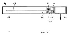
- Fig. 1 shows a radiation detector according to the present invention.
-
- An embodiment of a detector according to the present invention is shown in figure 1.
- The detector comprises an enclosure (22).
- Within the enclosure a photostimulable phosphor screen (23) is positioned. This screen for example comprises a divalent cesium halide phoshor, wherein said halide is at least one of chloride and bromide.
- The enclosure further comprises a source of stimulating light (24) arranged for stimulating said phosphor screen and an array of transducer elements (25) for capturing light emitted by the phoshor upon stimulation and for converting said light into an electrical signal representation.
- In the illustrated embodiment the source of stimulating light is implemented as a linear light source (more specifically an array of laser diodes) and the array of transducer elements is also a linear array (more specifically an array of charge coupled device elements). This embodiment can be made very compact and provides fast read out.
- The enclosure further comprises a linear erasing light source (26) arranged substantially parallel to the stimulating light source.
- The enclosure still further comprises means (not shown) for transporting the assembly (27) of stimulating light source, erasing light source and array of transducer elements relative to the phosphor screen in a so-called sub-scan direction, indicated by arrow (28).
- Means (29) are further provided for communicating the electrical signal representation output by the array of transducer elements to an external signal processing device.
- In this re-usable radiation detector the phosphor screen remains inside the enclosure during irradiation, read out and erasure.
- To garantee a low humidity the detector is flushed with N2. The gas is pumped out of a common recipient such as a gas cylinder into a first opening (30) in the enclosure (22). The gas is released into the air through a second opening (not shown) in enclosure (22).
- In this embodiment the stimulating light source and the array of transducer elements are arranged on opposite sides of the phosphor screen. In alternative embodiment these items may be arranged on the same side of the phosphor screen.
- The stimulable phosphor screen in the several embodiments of the present invention comprises a divalent europium activated cesium halide phosphor. Such a phosphor is known in the art and has for example been disclosed in EP-A-174 875 (and US 5,028,509). The phosphor is especially well suited for manufacturing 'binderless' phosphor screens. Binderless phosphor screens provide optimal sharpness.
- It is advantageous however to use a CsX:Eu phosphor wherein X represents a halide selected from the group consisting of Br and Cl, which is obtained by the following method:
- mixing CsX with between 10-3 and 5 mol % of a Europium compound selected from the group consisting of EuX'2, EuX'3 and EuOX', X' being a member selected from the group consisting of F, Cl, Br and I,
- firing the mixture at a temperature above 450 °C
- cooling said mixture and
- recovering the CsX:Eu phosphor.
- A phosphor that has been obtained as a result of the above method of preparation has an increased conversion efficiency compared to the state of the art divalent europium activated cesium halide phosphor. The phosphor can be stimulated by means of a lower amount of stimulation energy.
- A photostimulable phosphor screen using such a phosphor is preferably obtained by the method of
- preparing said CsX:Eu phosphor by firing a mixture of said CsX with between 10-3 and 5 mol % of an Europium compound selected from the group consisting of EuX'2, EuX'3 and EuOX', X' being a halide selected from the group consisting of F, Cl, Br and I and
- applying said phosphor on a substrate by a method selected from the group consisting of physical vapor deposition, thermal vapor deposition,, chemical vapor deposition, radio frequency deposition and pulsed laser deposition.
- This method of preparation is advantageous because it allows to deposit the phosphor in the form of needle-shaped crystals. These needle-shaped phosphor crystals act as light guides so that they reduce the lateral spreading of light in the phosphor layer. Reduced lateral light spread leads to images of higher resolution.
- Alternatively a phosphor screen containing a CsX:Eu stimulable phosphor, wherein X represents a halide selected from the group consisting of Br and Cl can also be manufactured by performing the steps of :
- bringing multiple containers of said CsX and an Europium compound selected from the group consisting of EuX'2, EuX'3 and EuOX', X' being a halide selected from the group consisting of F, Cl, Br and I in condition for vapor deposition and
- depositing, by a method selected from the group consisting of physical vapor deposition, thermal vapor deposition,, chemical vapor deposition, electron beam deposition, radio frequency deposition and pulsed laser deposition, both said CsX and said Europium compound on a substrate in such a ratio that on said substrate a CsX phosphor, doped with between 10-3 and 5 mol % of an Europium compound, is formed.
- This method of preparation is advantageous because it likewise allows to deposit the phosphor in the form of needle-shaped crystals. These needle-shaped phosphor crystals act as light guides so that they reduce the lateral spreading of light in the phosphor layer. Reduced lateral light spread leads to images of higher resolution.
- The above decribed phosphor and photostimulable phosphor screen have been described extensively in the following US provisional applications that are incorporated herein by reference: 60/159,004 and 60/142,276.
Claims (11)
- A radiation image detector comprisinga photostimulable phosphor screen,at least one source of stimulating light arranged for stimulating said phosphor screen,an array of transducer elements arranged for capturing light emitted by the phoshor screen upon stimulation and for converting said light into an electrical signal representation of said image,an enclosure enclosing said photostimulable phosphor screen, said assembly of stimulating light source and said array of transducer elements,interfacing means for communicating said electrical signal representation to an external signal processing device,means for preventing humidity from entering said enclosure.
- A radiation image detector according to claim 1 wherein said means for preventing humidity from entering said enclosure comprise means for flushing said enclosure with an inert gas.
- A radiation image detector according to claim 1 wherein said inert gas is N2.
- A radiation image detector according to claim 2 wherein said enclosure comprises a gas inlet arranged for coupling to a gas container and a gas outlet.
- A radiation image detector according to claim 2 wherein said means for flushing said enclosure with inert gas comprise means for circulating said gas inside said enclosure.
- A detector according to claim 1 wherein said linear stimulating light source is a linear array of laser diodes.
- A detector according to claim 1 wherein said linear array of transducer elements is a linear array of charge coupled device elements.
- A detector according to claim 1 wherein said phoshor screen comprises a divalent europium activated cesium halide phosphor wherein said halide is at least one of chloride and bromide.
- A detector according to claim 1 wherein said photostimulable phosphor screen is obtainable by the following steps:mixing CsX with between 10-3 and 5 mol % of a Europium compound selected from the group consisting of EuX'2, EuX'3 and EuOX', X' being a member selected from the group consisting of F, Cl, Br and I,firing the mixture at a temperature above 450 °Ccooling said mixture andrecovering the CsX:Eu phosphor.
- A detector according to claim 1 wherein said phosphor screen is obtained by the steps ofpreparing said CsX:Eu phosphor by firing a mixture of said CsX with between 10-3 and 5 mol % of an Europium compound selected from the group consisting of EuX'2, EuX'3 and EuOX', X' being a halide selected from the group consisting of F, Cl, Br and I andapplying said phosphor on a substrate by a method selected from the group consisting of physical vapour deposition, thermal vapour deposition, chemical vapour deposition, radio frequency deposition and pulsed laser deposition.
- A detector according to claim 1 wherein said phosphor screen is obtainable by the steps ofbringing multiple containers of said CsX and an Europium compound selected from the group consisting of EuX'2, EuX'3 and EuOX', X' being a halide selected from the group consisting of F, Cl, Br and I in condition for vapour deposition anddepositing, by a method selected from the group consisting of physical vapour deposition, thermal vapour deposition,, chemical vapour deposition, electron beam deposition, radio frequency deposition and pulsed laser deposition, both said CsX and said Europium compound on a substrate in such a ratio that on said substrate a CsX phosphor, doped with between 10-3 and 5 mol % of an Europium compound, is formed.
Applications Claiming Priority (5)
| Application Number | Priority Date | Filing Date | Title |
|---|---|---|---|
| US14227699P | 1999-07-02 | 1999-07-02 | |
| US142276P | 1999-07-02 | ||
| US15900499P | 1999-10-08 | 1999-10-08 | |
| US159004P | 1999-10-08 | ||
| US09/595,505 US6479835B1 (en) | 1999-07-02 | 2000-06-16 | Radiation image detector |
Publications (2)
| Publication Number | Publication Date |
|---|---|
| EP1065526A2 true EP1065526A2 (en) | 2001-01-03 |
| EP1065526A3 EP1065526A3 (en) | 2006-04-05 |
Family
ID=27385787
Family Applications (1)
| Application Number | Title | Priority Date | Filing Date |
|---|---|---|---|
| EP00202112A Withdrawn EP1065526A3 (en) | 1999-07-02 | 2000-06-13 | Radiation image detector |
Country Status (3)
| Country | Link |
|---|---|
| US (1) | US6479835B1 (en) |
| EP (1) | EP1065526A3 (en) |
| JP (1) | JP2001059897A (en) |
Cited By (1)
| Publication number | Priority date | Publication date | Assignee | Title |
|---|---|---|---|---|
| US6800870B2 (en) | 2000-12-20 | 2004-10-05 | Michel Sayag | Light stimulating and collecting methods and apparatus for storage-phosphor image plates |
Families Citing this family (6)
| Publication number | Priority date | Publication date | Assignee | Title |
|---|---|---|---|---|
| AU5750800A (en) * | 1999-07-02 | 2001-01-22 | Agfa-Gevaert Naamloze Vennootschap | Method for preparing a csx photostimulable phosphor and phosphors therefrom |
| US20010007352A1 (en) * | 1999-12-27 | 2001-07-12 | Erich Hell | Binderless storage phosphor screen with needle shaped crystals |
| JP2004163895A (en) * | 2002-09-25 | 2004-06-10 | Fuji Photo Film Co Ltd | Radiological image reader and excitation light cut filter |
| US20040081750A1 (en) * | 2002-10-25 | 2004-04-29 | Agfa-Gevaert | Storage phosphor screen and preparation method |
| US7075100B2 (en) * | 2003-09-22 | 2006-07-11 | Honeywell International Inc. | Confocal scanner system and method |
| JP2005200647A (en) * | 2003-12-19 | 2005-07-28 | Agfa Gevaert Nv | Mixing activator element homogeneously in storing phosphor |
Family Cites Families (10)
| Publication number | Priority date | Publication date | Assignee | Title |
|---|---|---|---|---|
| JPS59181335A (en) * | 1983-03-31 | 1984-10-15 | Fuji Photo Film Co Ltd | Signal detecting method in auto-radiography |
| JPS60217354A (en) * | 1984-04-13 | 1985-10-30 | Fuji Photo Film Co Ltd | Process for converting image of radiation |
| US5028509A (en) * | 1984-09-14 | 1991-07-02 | Konica Corporation | Method for converting radiographic image, radiation energy storage panel having stimulable phosphor-containing layer and alkali halide phosphor |
| DE3578081D1 (en) | 1984-09-14 | 1990-07-12 | Konishiroku Photo Ind | METHOD FOR CONVERTING A RADIOGRAPHIC IMAGE AND SCREEN FOR STORING RADIATION ENERGY WITH AN EXCITABLE PHOSPHORIC LAYER. |
| JPH0687114B2 (en) * | 1986-03-13 | 1994-11-02 | コニカ株式会社 | Radiation image information recording / reading device |
| US5023461A (en) * | 1987-08-18 | 1991-06-11 | Konica Corporation | Radiation image storage panel having low refractive index layer and protective layer |
| JP2843992B2 (en) * | 1988-06-24 | 1999-01-06 | コニカ株式会社 | Manufacturing method of radiation image conversion panel |
| IT1249543B (en) * | 1990-10-05 | 1995-02-28 | Minnesota Mining & Mfg | METHOD AND EQUIPMENT FOR READING A PHOTOSTIMULABLE PHOSPHORUS PANEL |
| WO1994028205A1 (en) * | 1993-05-25 | 1994-12-08 | Siemens Aktiengesellschaft | Process and device for producing large-surface crystalline salt plates |
| US5723865A (en) * | 1994-11-23 | 1998-03-03 | Thermotrex Corporation | X-ray imaging device |
-
2000
- 2000-06-13 EP EP00202112A patent/EP1065526A3/en not_active Withdrawn
- 2000-06-16 US US09/595,505 patent/US6479835B1/en not_active Expired - Fee Related
- 2000-06-29 JP JP2000195714A patent/JP2001059897A/en active Pending
Non-Patent Citations (1)
| Title |
|---|
| None * |
Cited By (3)
| Publication number | Priority date | Publication date | Assignee | Title |
|---|---|---|---|---|
| US6800870B2 (en) | 2000-12-20 | 2004-10-05 | Michel Sayag | Light stimulating and collecting methods and apparatus for storage-phosphor image plates |
| US7589341B2 (en) | 2000-12-20 | 2009-09-15 | Michel Sayag | Light stimulating and collecting methods and apparatus for storage-phosphor image plates |
| US7825394B2 (en) | 2000-12-20 | 2010-11-02 | Michel Sayag | Light stimulating and collecting methods and apparatus for storage-phosphor image plates |
Also Published As
| Publication number | Publication date |
|---|---|
| EP1065526A3 (en) | 2006-04-05 |
| US6479835B1 (en) | 2002-11-12 |
| JP2001059897A (en) | 2001-03-06 |
Similar Documents
| Publication | Publication Date | Title |
|---|---|---|
| EP0022564B1 (en) | Method of and apparatus for obtaining a radiation image by use of a stimulable phosphor | |
| US6504169B1 (en) | Method for reading a radiation image that has been stored in a photostimulable screen | |
| US6528812B1 (en) | Radiation image read-out method and apparatus | |
| US4641267A (en) | Gradation correction curve creating method and apparatus | |
| EP1065528A2 (en) | Radiation image read out method and apparatus | |
| US4585944A (en) | Radiation image storage panel | |
| US8405060B2 (en) | Radiation storage phosphor and applications | |
| EP0656169B1 (en) | Imaging system for mammography employing electron trapping materials | |
| US20030034458A1 (en) | Radiation image storage panel | |
| US6479835B1 (en) | Radiation image detector | |
| EP1471128A1 (en) | Stimulable cerium activated lutetium silicate phosphor | |
| EP0094678B1 (en) | Noise erasing method in radiation image recording and reproducing method | |
| US7211817B2 (en) | X-ray sensor | |
| US7439523B2 (en) | Method for preparing radiation image storage panel | |
| JPH05158174A (en) | Radiation image reader | |
| US7180086B2 (en) | System for reading out a plurality of differing storage phosphor screens | |
| JPS60157100A (en) | Method of converting radiation image | |
| EP1510564A1 (en) | Radiation image storage panel | |
| JP2509812B2 (en) | Storage device for radiation image conversion panel | |
| JPS61123829A (en) | Device for reading radiation image information | |
| US7335904B2 (en) | Process for read-out of radiation image | |
| JP2007010805A (en) | Method for discharging and removing radiation energy from radiograph conversion panel | |
| JPS62211638A (en) | Radiation image information recording and reading device | |
| JPS62218900A (en) | Radiation picture conversion element and method | |
| JP2002022895A (en) | Radiation image conversion panel |
Legal Events
| Date | Code | Title | Description |
|---|---|---|---|
| PUAI | Public reference made under article 153(3) epc to a published international application that has entered the european phase |
Free format text: ORIGINAL CODE: 0009012 |
|
| AK | Designated contracting states |
Kind code of ref document: A2 Designated state(s): AT BE CH CY DE DK ES FI FR GB GR IE IT LI LU MC NL PT SE |
|
| AX | Request for extension of the european patent |
Free format text: AL;LT;LV;MK;RO;SI |
|
| RAP1 | Party data changed (applicant data changed or rights of an application transferred) |
Owner name: AGFA-GEVAERT |
|
| PUAL | Search report despatched |
Free format text: ORIGINAL CODE: 0009013 |
|
| AK | Designated contracting states |
Kind code of ref document: A3 Designated state(s): AT BE CH CY DE DK ES FI FR GB GR IE IT LI LU MC NL PT SE |
|
| AX | Request for extension of the european patent |
Extension state: AL LT LV MK RO SI |
|
| 17P | Request for examination filed |
Effective date: 20061005 |
|
| AKX | Designation fees paid |
Designated state(s): DE FR GB |
|
| 17Q | First examination report despatched |
Effective date: 20061227 |
|
| RAP1 | Party data changed (applicant data changed or rights of an application transferred) |
Owner name: AGFA HEALTHCARE NV |
|
| STAA | Information on the status of an ep patent application or granted ep patent |
Free format text: STATUS: THE APPLICATION IS DEEMED TO BE WITHDRAWN |
|
| 18D | Application deemed to be withdrawn |
Effective date: 20070707 |