EP1063768B1 - DECT receiver with FM Demodulator - Google Patents
DECT receiver with FM Demodulator Download PDFInfo
- Publication number
- EP1063768B1 EP1063768B1 EP20000111285 EP00111285A EP1063768B1 EP 1063768 B1 EP1063768 B1 EP 1063768B1 EP 20000111285 EP20000111285 EP 20000111285 EP 00111285 A EP00111285 A EP 00111285A EP 1063768 B1 EP1063768 B1 EP 1063768B1
- Authority
- EP
- European Patent Office
- Prior art keywords
- resonant circuit
- quality
- demodulator
- takes place
- dect
- Prior art date
- Legal status (The legal status is an assumption and is not a legal conclusion. Google has not performed a legal analysis and makes no representation as to the accuracy of the status listed.)
- Expired - Lifetime
Links
Images


Classifications
-
- H—ELECTRICITY
- H03—ELECTRONIC CIRCUITRY
- H03D—DEMODULATION OR TRANSFERENCE OF MODULATION FROM ONE CARRIER TO ANOTHER
- H03D3/00—Demodulation of angle-, frequency- or phase- modulated oscillations
- H03D3/02—Demodulation of angle-, frequency- or phase- modulated oscillations by detecting phase difference between two signals obtained from input signal
- H03D3/06—Demodulation of angle-, frequency- or phase- modulated oscillations by detecting phase difference between two signals obtained from input signal by combining signals additively or in product demodulators
-
- H—ELECTRICITY
- H03—ELECTRONIC CIRCUITRY
- H03D—DEMODULATION OR TRANSFERENCE OF MODULATION FROM ONE CARRIER TO ANOTHER
- H03D3/00—Demodulation of angle-, frequency- or phase- modulated oscillations
- H03D3/26—Demodulation of angle-, frequency- or phase- modulated oscillations by means of sloping amplitude/frequency characteristic of tuned or reactive circuit
Definitions
- the present invention relates to a DECT receiver with a coincidence demodulator for FM-modulated signals, a method for calibrating a DECT receiver with a coincidence demodulator for FM-modulated signals.
- FM demodulation is FM-PDM (Pulse Width Modulation) conversion.
- a corresponding circuit arrangement is referred to as a coincidence demodulator or quadrature demodulator.
- Such a demodulation is shown for example in FIG Rudolf Maeusl, analog modulation method, Huetig Verlag, 1992 ,
- the frequency-modulated signal to be demodulated is divided into two paths and applied directly to a multiplier (mixer) via a frequency-dependent phase shifter which makes a phase shift of 90 ° at the carrier center frequency.
- a demodulation preceding amplitude limitation is required. Due to a strong amplitude limitation, which expediently acts on the two signals applied to the mixer, the function of the analog multiplier changes into that of a digital multiplier.
- the linearity of the FM demodulation is determined by the frequency dependence of the phase shift in the phase shifter.
- a linear relationship is obtained by means of a delay line in the form of an (ideal) Low pass filter, which is operated below its cutoff frequency.
- Less expensive is the execution of a phase shifter by a resonant circuit, which approximately in the vicinity of the resonant frequency is linear.
- the linear usable range becomes larger with low Q Q.
- FIG. 4 shows the basic circuit of a coincidence demodulator with a resonant circuit as a phase shifter.
- the coincidence demodulator shown has an amplitude limiter 8, an external resonant circuit 20, a mixer 9 and a low-pass filter 10 at the output of the mixer 9.
- the multiplier with u1 (t) is supplied to a limited to the amplitude rectangular voltage whose amplitude should have no influence on the output voltage
- the mean value obtained after integration is thus dependent on the phase shift of the two voltages u 1 (t) and u 2 (t) to each other and thus also dependent on the instantaneous frequency f FM (t) .
- quadrature demodulator derives from the “coincidence” or co-occurrence of the same positive or negative half waves of the voltages u 1 (t) and u 2 (t) to the multipliers, the result being a product of the voltages of whose phase assignment is dependent.
- quadrature demodulator refers to the voltages offset by 90 ° relative to one another at the carrier center frequency, that is to say in quadrature.
- a vote may e.g. by mechanical adjustment of the resonant circuit (adjustable capacitor) or by laser processing of capacitors.
- a quadrature demodulator in which the phase shift between the ones to be fed to a mixer Signals is generated by a low-pass filter whose quality is variable.
- the filter contains two antiparallel-connected diodes whose resistance varies signal-dependent.
- the disadvantage is that an adjustment of the quality of the demodulator depending on the operating state of the receiving device can not be done.
- the US 5,414,385 shows such a coincidence demodulator having a mixer which mixes a signal to be demodulated with a frequency-dependent phase-shifted branch, wherein the frequency-dependent phase shift is performed by a tunable in its quality resonant circuit.
- the present invention has as its object to provide a technique which facilitates calibration, i. the setting of the center frequency of the coincidence demodulator on the carrier frequency, specified.
- a DECT receiver with a coincidence demodulator for FM-modulated signals has a mixer (multiplier) which multiplies an FM modulated signal to be demodulated by a frequency-dependent phase-shifted branch of the signal to be demodulated.
- the quality Q of the resonant circuit is adjustable. The adjustment of the quality of the resonant circuit is controlled by a control voltage from a baseband block.
- the phase slope of the characteristic in the linear region is lower (the demodulator thus less sensitive), but for this the width of the linear region around the center frequency of the demodulator is greater.
- the carrier frequency of the transmitter with respect to the center frequency of the demodulator is the offset carrier frequency in the linear region of the demodulator and thus targeted a calibration process, ie the setting of the center frequency of the demodulator by changing the resonant frequency of the resonant circuit can be performed.
- the adjustment of the quality of the resonant circuit can be done by controlling a resistance value of a resistance of the resonant circuit.
- the adjustment of the quality of the resonant circuit can be done by turning on / off a transistor which is connected in parallel with a capacitor and an inductance of the resonant circuit.
- the adjustment of the quality of the resonant circuit can be done by turning on / off at least one transistor, which is connected to ground.
- the controllable resistor along with the mixer can be integrated on a chip as a building block.
- a method for calibrating a DECT receiver having a coincidence demodulator for FM modulated signals is done by adjusting the center frequency of the coincidence demodulator to reduce an offset voltage at the output of the coincidence demodulator.
- the quality of the resonant circuit is reduced in order to increase the width of the linear region of the demodulator.
- the reduction of the quality of the resonant circuit can be done by switching a transistor in its conductive state, wherein the transistor is connected in parallel with a capacitor and an inductance of the resonant circuit.
- the reduction of the quality of the resonant circuit can also be done by switching at least one transistor, wherein the transistor is connected to ground.
- the calibration can be carried out in particular during a time slot in a time-division multiplex system (for example the DECT standard) during which no modulated data is transmitted.
- time slots are also called “blind slots”.
- the invention relates to the application of the above method to the calibration of a DECT receiver with a coincidence demodulator for a transmission according to the DECT standard.
- a receiver branch for example, a DECT module.
- a signal received by an antenna 1 is passed through a filter 2 to a transmitting / receiving switch 3.
- the signal after a gain 4 and a further filtering 5 as a high-frequency signal to a mixer 6, which downs the received signal with the signal from a Lokaloszilator 21 to an intermediate frequency IF.
- the intermediate frequency signal IF is fed to an amplitude limiter 8.
- the external resonant circuit 22 connected in parallel with the amplitude limiter 8 suppresses broadband noise to improve the sensitivity of the receiver.
- an RSSI (radio signal strength indicator) signal 14 can be picked up at the amplitude limiter 8.
- the amplitude-limited signal from the amplitude limiter 8 is finally supplied to the coincidence demodulator 9.
- the output signal of the coincidence demodulator 9 is filtered 10 and then supplied to a comparator 12, which compares it with a reference voltage 11.
- the comparator 12 thus switches back and forth between two states and outputs this digitized output signal, which represents the demodulated information, to a base band block 13.
- the base band block 13 is thus connected downstream of the demodulator.
- the coincidence demodulator 9 is supplied with an unmodulated, ie a non-FM modulated signal.
- the output signal of the coincidence demodulator after integration should be as low as possible.
- a calibration unit 19 in the baseband block 13 detects the integrated output signal of the coincidence demodulator 9 and then changes the resonant frequency of the resonant circuit 20 so that the integrated output signal is pulled to zero.
- the change in the resonant frequency of the resonant circuit 20 can be achieved, for example, by adjusting a capacitor as in FIG FIG. 1 indicated or even by laser processing of a capacity done (once after the production of the coincidence demodulator. 9
- the carrier frequency of a transmitter with respect to the center frequency of the coincidence demodulator 9 may have an offset, as shown in FIG. 3 is shown.
- the center frequency f IF is the frequency at which the output signal corresponds to the reference voltage V REF .
- the carrier frequency of the RF signal inputted to the coincidence demodulator 9 is f TR , as in FIG. 3 As shown, the case may occur that this offset is so great that the carrier frequency f TR outside the linearity of the coincidence demodulator 9 is also in the case of the characteristic a.
- the characteristic curve of the coincidence demodulator 9 is changed in such a way during calibration that the linearity range of the coincidence demodulator 9 is increased. That can be like in FIG. 3 represented by switching to a "flatter" curve b done.
- the quality Q of the resonant circuit 20 is reduced according to the invention.
- S - 2 * Q f 0 .
- S is the phase slope of the transfer characteristic
- f 0 is the resonant frequency of the resonant circuit (substantially equal to the intermediate frequency f IF of the coincidence demodulator)
- Q is the quality of the resonant circuit.
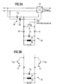
- FIG. 2a shows an embodiment of the controlled change, ie, for adjusting the Q of the resonant circuit 20.
- the resonant circuit has a capacitor C P , an inductance L P and a resistor R P.
- This actual resonant circuit 20 is in the implementation outside of an integrated chip and is connected via terminal pins 18 to the chip on which, for example, the mixer 15 is integrated.
- a MOS transistor 17 is provided, the control voltage is supplied for example from the baseband block 13. By switching on and off of the MOS transistor thus the Q of the resonant circuit can be changed.
- FIG. 2b shows a detail of FIG. 2a according to a further embodiment of the invention.
- at least one transistor 17 ', 17 " which is driven by the base band block 13, is connected to ground.
- two transistors 17', 17" connected to ground are shown, which are each switched to change the quality Q of the resonant circuit 20 , Alternatively, only one switched transistor can be provided, which is connected to ground.
- the characteristic a is obtained in the case that the MOS transistor 17 is turned off and the characteristic b when the MOS transistor 17 is turned on.
- the goodness Q of the resonant circuit 20 is changed by changing a resistance value.
- the calibration process may advantageously be done in the case of transmission in systems with time slots (as is the case for example with the DECT standard) during the so-called "blind slots" during which no FM-modulated information is transmitted.
- the baseband block 13, which is aware of the timing of the "blind slots" can thus advantageously also carry out the change in the characteristic curve of the coincidence demodulator for carrying out the calibration during the "blind slots".
Landscapes
- Engineering & Computer Science (AREA)
- Power Engineering (AREA)
- Digital Transmission Methods That Use Modulated Carrier Waves (AREA)
- Superheterodyne Receivers (AREA)
- Circuits Of Receivers In General (AREA)
- Stereo-Broadcasting Methods (AREA)
Description
Die vorliegende Erfindung betrifft einen DECT-Empfänger mit einem Koinzidenz-Demodulator für FM-modulierte Signale, ein Verfahren zur Kalibrierung eines DECT-Empfängers mit einem Koinzidenz-Demodulator für FM-modulierte Signale.The present invention relates to a DECT receiver with a coincidence demodulator for FM-modulated signals, a method for calibrating a DECT receiver with a coincidence demodulator for FM-modulated signals.
Eine Möglichkeit der FM-Demodulation ist die FM-PDM (Pulsdauermodulation)-Wandlung. Eine entsprechende Schaltungsanordnung wird als Koinzidenz-Demodulator oder auch Quadraturdemodulator bezeichnet. Eine derartige Demodulation ist beispielsweise dargestellt in
Bei der Koinzidenz-Demodulation wird das zu demodulierende frequenzmodulierte Signal auf zwei Pfade aufgeteilt und einmal direkt und zum anderen über ein frequenzabhängiges Phasendrehglied, das bei der Trägermittenfrequenz eine Phasendrehung um 90 DEG ausführt, auf einen Mulitiplizierer (Mischer) gegeben. Nachdem die Amplitude des Modulationsprodukts direkt in das demodulierte Signal eingeht, ist eine der Demodulation vorangehende Amplitudenbegrenzung erforderlich. Durch eine starke Amplitudenbegrenzung, die zweckmässigerweise auf die beiden am Mischer anliegenden Signale wirkt, geht die Funktion des analogen Multiplizierers in die eines digitalen Multiplizierers über.In coincidence demodulation, the frequency-modulated signal to be demodulated is divided into two paths and applied directly to a multiplier (mixer) via a frequency-dependent phase shifter which makes a phase shift of 90 ° at the carrier center frequency. After the amplitude of the modulation product directly enters the demodulated signal, a demodulation preceding amplitude limitation is required. Due to a strong amplitude limitation, which expediently acts on the two signals applied to the mixer, the function of the analog multiplier changes into that of a digital multiplier.
Die Linearität der FM-Demodulation wird bestimmt von der Frequenzabhängigkeit der Phasenverschiebung in dem Phasendrehglied. Einen linearen Zusammenhang erhält man mittels einer Laufzeitleitung in Form eines (idealen) Tiefpassfilters, das unterhalb seiner Grenzfrequenz betrieben wird. Weniger aufwendig ist die Ausführung eines Phasendrehglieds durch einen Schwingkreis, der in der Umgebung der Resonanzfrequenz näherungsweise linear ist. Der lineare ausnutzbare Bereich wird größer mit niedriger Kreisgüte Q.The linearity of the FM demodulation is determined by the frequency dependence of the phase shift in the phase shifter. A linear relationship is obtained by means of a delay line in the form of an (ideal) Low pass filter, which is operated below its cutoff frequency. Less expensive is the execution of a phase shifter by a resonant circuit, which approximately in the vicinity of the resonant frequency is linear. The linear usable range becomes larger with low Q Q.
Der Name "Koinzidenz-Demodulator" leitet sich ab von dem "Zusammentreffen" oder gleichzeitigem Anliegen von den gleichsinnigen positiven oder negativen Halbwellen der Spannungen u1(t) und u2(t) an die Multiplizierer, wobei das Ergebnis als Produkt der Spannungen von deren Phasenzuordnung abhängig ist. Ein anderer Name, "Quadraturdemodulator", nimmt Bezug auf die bei der Trägermittenfrequenz um 90° zueinander versetzten, also in "Quadratur" zustehenden Spannungen.The name "coincidence demodulator" derives from the "coincidence" or co-occurrence of the same positive or negative half waves of the voltages u 1 (t) and u 2 (t) to the multipliers, the result being a product of the voltages of whose phase assignment is dependent. Another name, quadrature demodulator, refers to the voltages offset by 90 ° relative to one another at the carrier center frequency, that is to say in quadrature.
Aufgrund von Toleranzen der Bauelemente muß der Schwingkreis 20 genau auf die Trägerfrequenz des zugeführten, frequenzmodulierten Signals abgestimmt werden. Eine solche Abstimmung kann z.B. durch mechanische Justierung des Schwingkreises (einstellbarer Kondensator) oder durch Laserbearbeitung von Kondensatoren erfolgen.Due to tolerances of the components of the
In der
Die
Die vorliegende Erfindung hat es sich zur Aufgabe gemacht, eine Technik bereitzustellen, die die Kalibrierung, d.h. die Einstellung der Mittenfrequenz des Koinzidenz-Demodulators auf die Trägerfrequenz, präzisiert.The present invention has as its object to provide a technique which facilitates calibration, i. the setting of the center frequency of the coincidence demodulator on the carrier frequency, specified.
Diese Aufgabe wird erfindungsgemäß durch die Merkmale der unabhängigen Ansprüche gelöst. Die abhängigen Ansprüche bilden den zentralen Gedanken der Erfindung in besonders vorteilhafter Weise weiter.This object is achieved by the features of the independent claims. The dependent claims further form the central idea of the invention in a particularly advantageous manner.
Gemäß der vorliegenden Erfindung ist also ein DECT-Empfänger mit einem Koinzidenz-Demodulator für FM-modulierte Signale vorgesehen. Der Koinzidenz-Demodulator weist einen Mischer (Multiplizierer) auf, der ein zu demodulierendes (FM-moduliertes) Signal mit einem frequenzabhängig phasenverschobenen Zweig des zu demodulierenden Signal multipliziert. Durch einen Schwingkreis erfolgt dabei die frequenzabhängige Phasenverschiebung. Die Güte Q des Schwingkreises ist dabei einstellbar. Die Einstellung der Güte des Schwingkreises wird durch eine Steuerspannung von einem Basisbandblock gesteuert. Durch Einstellen der Güte des Schwingkreises kann somit die Kennlinie des Demodulators, genauer gesagt die Breite des Bereichs um die Mittenfrequenz des Demodulators herum, verändert werden. Bei kleinerer Güte ist die Phasensteilheit der Kennlinie in dem linearen Bereich niedriger (der Demodulator somit weniger sensitiv), aber dafür die Breite des linearen Bereichs um die Mittenfrequenz des Demodulators herum größer. Somit kann bei einem Kalibriervorgang besser gewährleistet werden, dass auch bei einem größeren Offset beispielsweise der Trägerfrequenz des Senders bezüglich der Mittenfrequenz des Demodulators sich die versetzte Trägerfrequenz im linearen Bereich des Demodulators befindet und somit gezielt ein Kalibrierungsvorgang, d.h. die Einstellung der Mittenfrequenz des Demodulators durch Veränderung der Resonanzfrequenz des Schwingkreises ausgeführt werden kann.According to the present invention, therefore, a DECT receiver with a coincidence demodulator for FM-modulated signals is provided. The coincidence demodulator has a mixer (multiplier) which multiplies an FM modulated signal to be demodulated by a frequency-dependent phase-shifted branch of the signal to be demodulated. By a resonant circuit while the frequency-dependent phase shift takes place. The quality Q of the resonant circuit is adjustable. The adjustment of the quality of the resonant circuit is controlled by a control voltage from a baseband block. Thus, by adjusting the quality of the resonant circuit, the characteristic of the demodulator, more specifically the width of the region around the center frequency of the demodulator, can be changed. With a lower quality, the phase slope of the characteristic in the linear region is lower (the demodulator thus less sensitive), but for this the width of the linear region around the center frequency of the demodulator is greater. Thus, it can be better ensured in a calibration process that even with a larger offset, for example, the carrier frequency of the transmitter with respect to the center frequency of the demodulator is the offset carrier frequency in the linear region of the demodulator and thus targeted a calibration process, ie the setting of the center frequency of the demodulator by changing the resonant frequency of the resonant circuit can be performed.
Die Einstellung der Güte des Schwingkreises kann durch Steuerung eines Widerstandswerts eines Widerstands des Schwingkreises erfolgen.The adjustment of the quality of the resonant circuit can be done by controlling a resistance value of a resistance of the resonant circuit.
Die Einstellung der Güte des Schwingkreises kann durch Ein/Ausschalten eines Transistors erfolgen, der parallel zu einem Kondensator und einer Induktivität des Schwingkreises geschaltet ist.The adjustment of the quality of the resonant circuit can be done by turning on / off a transistor which is connected in parallel with a capacitor and an inductance of the resonant circuit.
Die Einstellung der Güte des Schwingkreises kann durch Ein/Ausschalten wenigstens eines Transistors erfolgen, der gegen Masse geschaltet ist.The adjustment of the quality of the resonant circuit can be done by turning on / off at least one transistor, which is connected to ground.
Der steuerbare Widerstand zusammen mit dem Mischer auf einem Chip als Baustein integriert werden.The controllable resistor along with the mixer can be integrated on a chip as a building block.
Gemäß der vorliegenden Erfindung ist weiterhin ein Verfahren zur Kalibrierung eines DECT-Empfängers, der einen Koinzidenz-Demodulator für FM-modulierte Signale aufweist, vorgesehen. Die Kalibrierung erfolgt durch Justierung der Mittenfrequenz des Koinzidenz-Demodulators zur Verringerung einer OffsetSpannung am Ausgang des Koinzidenz-Demodulators. Dabei wird während der Kalibrierung die Güte des Schwingkreises verringert, um die Breite des Linearbereichs des Demodulators zu vergrößern.In accordance with the present invention, there is still a method for calibrating a DECT receiver having a coincidence demodulator for FM modulated signals. The calibration is done by adjusting the center frequency of the coincidence demodulator to reduce an offset voltage at the output of the coincidence demodulator. During the calibration, the quality of the resonant circuit is reduced in order to increase the width of the linear region of the demodulator.
Die Verringerung der Güte des Schwingkreises kann durch Schalten eines Transistors in seinem leitfähigen Zustand erfolgen, wobei der Transistor parallel zu einem Kondensator und einer Induktivität des Schwingkreises geschaltet ist.The reduction of the quality of the resonant circuit can be done by switching a transistor in its conductive state, wherein the transistor is connected in parallel with a capacitor and an inductance of the resonant circuit.
Die Verringerung der Güte des Schwingkreises kann auch durch Schalten wenigstens eines Transistors erfolgen, wobei der Transistor gegen Masse geschaltet ist.The reduction of the quality of the resonant circuit can also be done by switching at least one transistor, wherein the transistor is connected to ground.
Die Kalibrierung kann insbesondere während eines Zeitschlitzes in einem Zeitmultiplex-System (beispielsweise dem DECT-Standard) erfolgen, während dem keine modulierten Daten übertragen werden. Derartige Zeitschlitze werden auch "blind slots" genannt.The calibration can be carried out in particular during a time slot in a time-division multiplex system (for example the DECT standard) during which no modulated data is transmitted. Such time slots are also called "blind slots".
Die Erfindung betrifft die Anwendung des oben genannten Verfahrens auf die Kalibrierung eines DECT-Empfängers mit einem Koinzidenz-Demodulator für eine Übertragung gemäß dem DECT-Standard.The invention relates to the application of the above method to the calibration of a DECT receiver with a coincidence demodulator for a transmission according to the DECT standard.
Weitere Vorteile, Merkmale und Eigenschaften der vorliegenden Erfindung werden aus der folgenden Beschreibung von Ausführungsbeispielen und bezugnehmend auf die begleitenden Figuren der Zeichnungen näher ersichtlich.
-
Fig. 1 zeigt einen Empfängerzweig mit einem Koinzidenz-Demodulator, -
Fig. 2a zeigt einen Koinzidenz-Demodulator eines DECT-Empfängers gemäß der vorliegenden Erfindung, -
Fig. 2b zeigt einen Ausschnitt vonFig. 2a gemäß einem weiteren Ausführungsbeispiel der Erfindung, -
Fig. 3 zeigt die einstellbare Kennlinie eines Koinzidenz-Demodulators eines erfindungsgemäßen DECT-Empfängers, undFig. 4 zeigt eine allgemeine aus dem Stand der Technik bekannte Darstellung eines Koinzidenz-Demodulators.
-
Fig. 1 shows a receiver branch with a coincidence demodulator, -
Fig. 2a shows a coincidence demodulator of a DECT receiver according to the present invention, -
Fig. 2b shows a section ofFig. 2a according to a further embodiment of the invention, -
Fig. 3 shows the adjustable characteristic of a coincidence demodulator of a DECT receiver according to the invention, andFig. 4 Figure 4 shows a general prior art representation of a coincidence demodulator.
Bezugnehmend auf
Das amplitudenbegrenzte Signal von dem Amplitudenbegrenzer 8 wird schließlich dem Koinzidenz-Demodulator 9 zugeführt. Das Ausgangssignal des Koinzidenz-Demodulators 9 wird gefiltert 10 und dann einem Komparator 12 zugeführt, der es mit einer Referenzspannung 11 vergleicht. Der Komparator 12 schaltet somit zwischen zwei Zuständen hin- und her und gibt dieses digitalisierte Ausgangssignal, daß die demodulierte Information darstellt, zu einem Basisbandblock 13. Der Basisbandblock 13 ist dem Demodulator also nachgeschaltet.The amplitude-limited signal from the amplitude limiter 8 is finally supplied to the
Während einer Kalibrierung, d.h. einer Einstellung der Mittenfrequenz des Koinzidenz-Demodulators 9 auf die tatsächliche Trägerfrequenz, die von einem Sender verwendet wird, wird dem Koinzidenz-Demodulator 9 ein unmoduliertes, d.h. ein nicht FM-moduliertes Signal zugeführt. In diesem Zustand sollte das Ausgangssignal des Koinzidenz-Demodulators nach der Integration 10 möglichst 0 betragen. Eine Kalibriereinheit 19 im Basisbandblock 13 erfaßt das integrierte Ausgangssignal des Koinzidenz-Demodulators 9 und verändert dann die Resonanzfrequenz des Schwingkreises 20 derart, daß das integrierte Ausgangssignal auf 0 gezogen wird. Die Änderung der Resonanzfrequenz des Schwingkreises 20 kann beispielsweise durch Einstellen eines Kondensators wie in
Wie bereits gesagt, kann die Trägerfrequenz eines Senders bezüglich der Mittenfrequenz des Koinzidenz-Demodulators 9 einen Offset aufweisen, wie es in
Außerhalb des Linearitätsbereichs ist indessen der Kalibriervorgang kaum möglich, da ja eine Verschiebung der Mittenfrequenz des Koinzidenz-Demodulators 9 um einen gewissen Differenzwert für diesen genannten Fall keine Änderung der Ausgangsspannung bewirkt.However, outside the linearity range, the calibration process is hardly possible, since a shift of the center frequency of the
Erfindungsgemäß wird daher bei der Kalibrierung die Kennlinie des Koinzidenz-Demodulators 9 derart geändert, daß der Linearitätsbereich des Koinzidenz-Demodulators 9 vergrößert wird. Das kann wie in 

wobei S die Phasensteilheit der Übertragungskennlinie, f0 die Resonanzfrequenz des Schwingkreises (im wesentlichen gleich der Zwischenfrequenz fZF des Koinzidenz-Demodulators) und Q die Güte des Schwingkreises ist.According to the invention, therefore, the characteristic curve of the
where S is the phase slope of the transfer characteristic, f 0 is the resonant frequency of the resonant circuit (substantially equal to the intermediate frequency f IF of the coincidence demodulator) and Q is the quality of the resonant circuit.
Zur Veränderung der Güte Q des Schwingkreises 20 ist ein MOS-Transistor 17 vorgesehen, dessen Steuerspannung beispielsweise vom Basisbandblock 13 zugeführt wird. Durch Ein-und Ausschalten des MOS-Transistors kann somit die Güte Q des Schwingkreises verändert werden.To change the quality Q of the
Bezugnehmend nochmals auf
Der Kalibrierungsvorgang kann vorteilhafterweise für den Fall von Übertragung in Systemen mit Zeitschlitzen (wie es beispielsweise bei dem DECT-Standard der Fall ist) während der sogenannten "blind slots" erfolgen, während der keine FM-modulierte Information übertragen wird. Der Basisbandblock 13, dem die zeitliche Lage der "blind slots" bekannt ist, kann somit vorteilhafterweise auch das die Veränderung der Kennlinie des Koinzidenz-Demodulators zur Ausführung der Kalibrierung während der "blind slots" durchführen.The calibration process may advantageously be done in the case of transmission in systems with time slots (as is the case for example with the DECT standard) during the so-called "blind slots" during which no FM-modulated information is transmitted. The
- 1. Antenne1. Antenna
- 2. Sende/Empfangs-Filter2. Transmit / receive filter
- 3. Sende/Empfangs-Weiche3. Transceiver
- 4. LNA-Verstärker4. LNA amplifier
- 5. HF-Filter5. RF filter
- 6. Mischer6. Mixer
- 7. IF-Filter7. IF filter
- 8. Amplitudenbegrenzer8. Amplitude limiter
- 9. Koinzidenz-Demodulator9. coincidence demodulator
- 10. Filter10. Filter
- 11. Referenzspannung11. Reference voltage
- 12. Komparator12. Comparator
- 13. Basisbandblock13. Baseband block
- 14. RSSI-Signal14. RSSI signal
- 15. Multiplizierer15. Multiplier
- 16. Koppelkondensator16. Coupling capacitor
- 17. MOS-Transistor17th MOS transistor
- 17'. Transistor gegen Masse (geschaltet)17 '. Transistor to ground (switched)
- 17''. Transistor gegen Masse (geschaltet)17 ''. Transistor to ground (switched)
- 18. Pin18th pin
- 19. Kalibriereinheit19. Calibration unit
- 20. Schwingkreis20. Oscillating circuit
- 21. Lokaloszilator21. Local oscillator
- 22. Schwingkreis des Amplitudenbegrenzers22. Oscillating circuit of the amplitude limiter
Claims (10)
- DECT-receiver,
characterized in that
it comprises a coincidence demodulator for FM-modulated signals,
the coincidence demodulator comprising a mixer (15), which mixes a signal to be demodulated with a frequency dependent phase-shifted branch of the signal to be demodulated, wherein
the frequency dependent phase shift takes place by a resonant circuit (20), the quality of which is adjustable, and wherein
the adjustment of the quality of the resonant circuit (20) is controlled by a base band block (13) downstream connected to the demodulator. - DECT-receiver according to claim 1,
characterized in that
the adjustment of the quality of the resonant circuit (20) takes place by controlling the resistance value of a resistor (17, Rp) of the resonant circuit (20). - DECT-receiver according to claim 1 or 2,
characterized in that
the adjustment of the quality of the resonant circuit (20) takes place by switching on/out a transistor (17), which is connected in parallel to a capacity (Cp) and an inductivity (Lp). - DECT-receiver according to claim 1 or 2,
characterized in that
the adjustment of the quality of the resonant circuit (20) takes place by switching on/out at least one transistor (17', 17"), which is switched against ground. - DECT-receiver according to claim 2,
characterized in that
the controllable resistor (17) is integrated with the mixer (15) on a chip. - Method for calibration of a DECT-receiver, which comprises a coincidence demodulator for FM-modulated signals,
wherein the coincidence demodulator comprises a mixer (15), which mixes a signal to be demodulated with a frequency dependent phase-shifted branch of the signal to be demodulated,
wherein the frequency dependent phase shift takes place by a resonant circuit (20), the quality of which is adjustable,
characterized in that
the calibration takes place by adjusting the center frequency of the coincidence demodulator (9) for reducing an offset voltage at the output of the coincidence demodulator (9) and a quality of the resonant circuit (20) is reduced before the calibration. - Method according to claim 6,
characterized in that
the reduction of the quality of the resonant circuit (20) takes place by changing a resistance value of a resistor (17, Rp) of the resonant circuit (20). - Method according to claim 6 or 7,
characterized in that
the reduction of the quality of the resonant circuit (20) takes place by switching a transistor (17) to its conductive state, wherein the transistor (17) is connected in parallel to a capacity (Cp) and an inductivity (Lp). - Method according to claim 6 or 7,
characterized in that
the reduction of the quality of the resonant circuit (20) takes place by switching at least one transistor (17', 17"), which is connected against ground. - Method according to one of the claims 6 to 9,
characterized in that
the calibration during a time slot takes place in a time multiplex system, during which no modulated data are transmitted.
Applications Claiming Priority (2)
| Application Number | Priority Date | Filing Date | Title |
|---|---|---|---|
| DE19928546 | 1999-06-22 | ||
| DE19928546 | 1999-06-22 |
Publications (3)
| Publication Number | Publication Date |
|---|---|
| EP1063768A2 EP1063768A2 (en) | 2000-12-27 |
| EP1063768A3 EP1063768A3 (en) | 2002-09-18 |
| EP1063768B1 true EP1063768B1 (en) | 2010-09-29 |
Family
ID=7912133
Family Applications (1)
| Application Number | Title | Priority Date | Filing Date |
|---|---|---|---|
| EP20000111285 Expired - Lifetime EP1063768B1 (en) | 1999-06-22 | 2000-05-25 | DECT receiver with FM Demodulator |
Country Status (2)
| Country | Link |
|---|---|
| EP (1) | EP1063768B1 (en) |
| DE (1) | DE50016001D1 (en) |
Family Cites Families (7)
| Publication number | Priority date | Publication date | Assignee | Title |
|---|---|---|---|---|
| GB1421093A (en) * | 1974-05-09 | 1976-01-14 | Mullard Ltd | Frequency discriminator circuit arrangement |
| GB2001217B (en) * | 1977-07-15 | 1982-01-27 | Victor Company Of Japan | Phase tracked loop frequency demodulator |
| US4342000A (en) * | 1979-04-04 | 1982-07-27 | Nippon Gakki Seizo Kabushiki Kaisha | FM Detecting circuit |
| US4451792A (en) * | 1981-10-23 | 1984-05-29 | Motorola, Inc. | Auto-tuned frequency discriminator |
| DE3419602A1 (en) * | 1984-05-25 | 1985-11-28 | Philips Patentverwaltung Gmbh, 2000 Hamburg | CIRCUIT ARRANGEMENT FOR REDUCING DISTORTIONS IN AN FM SQUARE DETECTOR |
| US5293135A (en) * | 1992-12-31 | 1994-03-08 | Motorola, Inc. | FM demodulator with self-tuning quadrature detector |
| US5414385A (en) * | 1994-02-22 | 1995-05-09 | Matsushita Communication Industrial Corporation Of America | Dual mode FM quadrature detector |
-
2000
- 2000-05-25 EP EP20000111285 patent/EP1063768B1/en not_active Expired - Lifetime
- 2000-05-25 DE DE50016001T patent/DE50016001D1/en not_active Expired - Lifetime
Also Published As
| Publication number | Publication date |
|---|---|
| EP1063768A2 (en) | 2000-12-27 |
| DE50016001D1 (en) | 2010-11-11 |
| EP1063768A3 (en) | 2002-09-18 |
Similar Documents
| Publication | Publication Date | Title |
|---|---|---|
| DE69737000T2 (en) | Radio transmitter Receiver for sending and receiving MF signals in two bands | |
| DE4191766C2 (en) | Frequency control circuit for an adjustable receiver oscillator | |
| DE69838381T2 (en) | TWO BAND RADIO RECEIVER | |
| EP0981864B1 (en) | Integrable radio receiver circuit for frequency-modulated digital signals | |
| DE69329140T2 (en) | Direct conversion recipient | |
| DE3885625T2 (en) | Earth and satellite broadcast receivers. | |
| DE69735335T2 (en) | Removal of the DC offset and suppression of corrupted AM signals in a direct conversion receiver | |
| DE60022159T2 (en) | Transmitter with closed feedback for modulation | |
| DE60205983T2 (en) | demodulator | |
| EP0720800B1 (en) | High-frequency receiver | |
| DE2142660A1 (en) | Tuning and reception field strength display circuit | |
| EP1568143A1 (en) | Transmission stage comprising phases and an amplitude regulating loop | |
| DE19734265C2 (en) | TV tuner | |
| DE102005004105B4 (en) | Signal processing device and method for operating a signal processing device | |
| EP0727905B1 (en) | Multi-standard television receiver | |
| DE60024188T2 (en) | Receiver for analog and digital radio reception | |
| DE2831091C2 (en) | Frequency demodulator with a phase tracking loop | |
| EP1063768B1 (en) | DECT receiver with FM Demodulator | |
| EP1128552B1 (en) | Circuit device for filtering a radio frequency signal | |
| DE69818075T2 (en) | SIGNAL PROCESSING SYSTEM | |
| DE60027028T2 (en) | FSK DEMODULATOR USING A FREQUENCY TRANSFER WITH THREE PARALLEL SWITCHED MIXERS | |
| DE3412191C2 (en) | ||
| EP1216558B1 (en) | Transmitting-receiving device comprising a closed cartesian feedback loop | |
| DE69215737T2 (en) | Radio reception systems | |
| DE4017418A1 (en) | Double tuner type radio receiver - has two oscillators selectively coupled to phase detector, filter, smoothing circuit and divider to form two PLL-circuits |
Legal Events
| Date | Code | Title | Description |
|---|---|---|---|
| PUAI | Public reference made under article 153(3) epc to a published international application that has entered the european phase |
Free format text: ORIGINAL CODE: 0009012 |
|
| AK | Designated contracting states |
Kind code of ref document: A2 Designated state(s): AT BE CH CY DE DK ES FI FR GB GR IE IT LI LU MC NL PT SE |
|
| AX | Request for extension of the european patent |
Free format text: AL;LT;LV;MK;RO;SI |
|
| PUAL | Search report despatched |
Free format text: ORIGINAL CODE: 0009013 |
|
| AK | Designated contracting states |
Kind code of ref document: A3 Designated state(s): AT BE CH CY DE DK ES FI FR GB GR IE IT LI LU MC NL PT SE |
|
| AX | Request for extension of the european patent |
Free format text: AL;LT;LV;MK;RO;SI |
|
| RIN1 | Information on inventor provided before grant (corrected) |
Inventor name: LI PUMA, GUISEPPE |
|
| 17P | Request for examination filed |
Effective date: 20030318 |
|
| AKX | Designation fees paid |
Designated state(s): DE FR GB |
|
| 17Q | First examination report despatched |
Effective date: 20070711 |
|
| RAP1 | Party data changed (applicant data changed or rights of an application transferred) |
Owner name: INFINEON TECHNOLOGIES AG |
|
| GRAP | Despatch of communication of intention to grant a patent |
Free format text: ORIGINAL CODE: EPIDOSNIGR1 |
|
| RTI1 | Title (correction) |
Free format text: DECT RECEIVER WITH FM DEMODULATOR |
|
| GRAS | Grant fee paid |
Free format text: ORIGINAL CODE: EPIDOSNIGR3 |
|
| GRAA | (expected) grant |
Free format text: ORIGINAL CODE: 0009210 |
|
| AK | Designated contracting states |
Kind code of ref document: B1 Designated state(s): DE FR GB |
|
| REG | Reference to a national code |
Ref country code: GB Ref legal event code: FG4D Free format text: NOT ENGLISH |
|
| REF | Corresponds to: |
Ref document number: 50016001 Country of ref document: DE Date of ref document: 20101111 Kind code of ref document: P |
|
| PLBE | No opposition filed within time limit |
Free format text: ORIGINAL CODE: 0009261 |
|
| STAA | Information on the status of an ep patent application or granted ep patent |
Free format text: STATUS: NO OPPOSITION FILED WITHIN TIME LIMIT |
|
| 26N | No opposition filed |
Effective date: 20110630 |
|
| REG | Reference to a national code |
Ref country code: DE Ref legal event code: R097 Ref document number: 50016001 Country of ref document: DE Effective date: 20110630 |
|
| GBPC | Gb: european patent ceased through non-payment of renewal fee |
Effective date: 20110525 |
|
| REG | Reference to a national code |
Ref country code: FR Ref legal event code: ST Effective date: 20120131 |
|
| PG25 | Lapsed in a contracting state [announced via postgrant information from national office to epo] |
Ref country code: FR Free format text: LAPSE BECAUSE OF NON-PAYMENT OF DUE FEES Effective date: 20110531 |
|
| PG25 | Lapsed in a contracting state [announced via postgrant information from national office to epo] |
Ref country code: GB Free format text: LAPSE BECAUSE OF NON-PAYMENT OF DUE FEES Effective date: 20110525 |
|
| REG | Reference to a national code |
Ref country code: GB Ref legal event code: 732E Free format text: REGISTERED BETWEEN 20120614 AND 20120620 |
|
| REG | Reference to a national code |
Ref country code: GB Ref legal event code: 732E Free format text: REGISTERED BETWEEN 20121213 AND 20121219 |
|
| REG | Reference to a national code |
Ref country code: DE Ref legal event code: R081 Ref document number: 50016001 Country of ref document: DE Owner name: INTEL MOBILE COMMUNICATIONS GMBH, DE Free format text: FORMER OWNER: INFINEON TECHNOLOGIES AG, 85579 NEUBIBERG, DE Effective date: 20130314 Ref country code: DE Ref legal event code: R081 Ref document number: 50016001 Country of ref document: DE Owner name: INTEL MOBILE COMMUNICATIONS GMBH, DE Free format text: FORMER OWNER: INFINEON TECHNOLOGIES AG, 85579 NEUBIBERG, DE Effective date: 20130315 Ref country code: DE Ref legal event code: R081 Ref document number: 50016001 Country of ref document: DE Owner name: INTEL MOBILE COMMUNICATIONS GMBH, DE Free format text: FORMER OWNER: INTEL MOBILE COMMUNICATIONS GMBH, 85579 NEUBIBERG, DE Effective date: 20130315 Ref country code: DE Ref legal event code: R081 Ref document number: 50016001 Country of ref document: DE Owner name: INTEL MOBILE COMMUNICATIONS GMBH, DE Free format text: FORMER OWNER: INTEL MOBILE COMMUNICATIONS TECHNOLOGY GMBH, 85579 NEUBIBERG, DE Effective date: 20130326 |
|
| PGFP | Annual fee paid to national office [announced via postgrant information from national office to epo] |
Ref country code: DE Payment date: 20150519 Year of fee payment: 16 |
|
| REG | Reference to a national code |
Ref country code: DE Ref legal event code: R119 Ref document number: 50016001 Country of ref document: DE |
|
| PG25 | Lapsed in a contracting state [announced via postgrant information from national office to epo] |
Ref country code: DE Free format text: LAPSE BECAUSE OF NON-PAYMENT OF DUE FEES Effective date: 20161201 |