EP1063669A2 - Cathode with improved work function and method for making the same - Google Patents
Cathode with improved work function and method for making the same Download PDFInfo
- Publication number
- EP1063669A2 EP1063669A2 EP00305015A EP00305015A EP1063669A2 EP 1063669 A2 EP1063669 A2 EP 1063669A2 EP 00305015 A EP00305015 A EP 00305015A EP 00305015 A EP00305015 A EP 00305015A EP 1063669 A2 EP1063669 A2 EP 1063669A2
- Authority
- EP
- European Patent Office
- Prior art keywords
- buffer
- substrate
- cathode
- thermoionic
- thermoionic cathode
- Prior art date
- Legal status (The legal status is an assumption and is not a legal conclusion. Google has not performed a legal analysis and makes no representation as to the accuracy of the status listed.)
- Granted
Links
- 238000000034 method Methods 0.000 title claims description 13
- 239000000758 substrate Substances 0.000 claims abstract description 74
- 238000000151 deposition Methods 0.000 claims abstract description 8
- 239000006104 solid solution Substances 0.000 claims abstract description 8
- 238000004519 manufacturing process Methods 0.000 claims abstract description 7
- 229910045601 alloy Inorganic materials 0.000 claims abstract description 3
- 239000000956 alloy Substances 0.000 claims abstract description 3
- 229910052715 tantalum Inorganic materials 0.000 claims description 25
- GUVRBAGPIYLISA-UHFFFAOYSA-N tantalum atom Chemical compound [Ta] GUVRBAGPIYLISA-UHFFFAOYSA-N 0.000 claims description 23
- 238000000137 annealing Methods 0.000 claims description 8
- 229910052750 molybdenum Inorganic materials 0.000 claims description 7
- 229910052702 rhenium Inorganic materials 0.000 claims description 7
- 229910052721 tungsten Inorganic materials 0.000 claims description 7
- 230000015572 biosynthetic process Effects 0.000 claims description 6
- 229910052799 carbon Inorganic materials 0.000 claims description 6
- 238000009792 diffusion process Methods 0.000 claims description 6
- 238000004544 sputter deposition Methods 0.000 claims description 6
- 238000005275 alloying Methods 0.000 claims description 5
- 238000001556 precipitation Methods 0.000 claims description 5
- 239000003870 refractory metal Substances 0.000 claims description 5
- OKTJSMMVPCPJKN-UHFFFAOYSA-N Carbon Chemical compound [C] OKTJSMMVPCPJKN-UHFFFAOYSA-N 0.000 claims description 4
- ZOKXTWBITQBERF-UHFFFAOYSA-N Molybdenum Chemical compound [Mo] ZOKXTWBITQBERF-UHFFFAOYSA-N 0.000 claims description 4
- 230000008021 deposition Effects 0.000 claims description 4
- 238000001459 lithography Methods 0.000 claims description 4
- 239000011733 molybdenum Substances 0.000 claims description 4
- WUAPFZMCVAUBPE-UHFFFAOYSA-N rhenium atom Chemical compound [Re] WUAPFZMCVAUBPE-UHFFFAOYSA-N 0.000 claims description 4
- 239000000126 substance Substances 0.000 claims description 4
- WFKWXMTUELFFGS-UHFFFAOYSA-N tungsten Chemical compound [W] WFKWXMTUELFFGS-UHFFFAOYSA-N 0.000 claims description 4
- 239000010937 tungsten Substances 0.000 claims description 4
- 229910052741 iridium Inorganic materials 0.000 claims description 2
- 229910052758 niobium Inorganic materials 0.000 claims description 2
- 229910052703 rhodium Inorganic materials 0.000 claims description 2
- 238000000992 sputter etching Methods 0.000 claims description 2
- 229910052720 vanadium Inorganic materials 0.000 claims description 2
- 230000000903 blocking effect Effects 0.000 claims 4
- 238000006243 chemical reaction Methods 0.000 claims 4
- 229910052735 hafnium Inorganic materials 0.000 claims 3
- 229910052762 osmium Inorganic materials 0.000 claims 3
- 229910052707 ruthenium Inorganic materials 0.000 claims 3
- 238000004090 dissolution Methods 0.000 claims 1
- 230000002401 inhibitory effect Effects 0.000 claims 1
- 229910052713 technetium Inorganic materials 0.000 claims 1
- 239000013078 crystal Substances 0.000 abstract description 5
- 239000010410 layer Substances 0.000 description 50
- 239000000463 material Substances 0.000 description 23
- 239000012528 membrane Substances 0.000 description 11
- PXHVJJICTQNCMI-UHFFFAOYSA-N Nickel Chemical compound [Ni] PXHVJJICTQNCMI-UHFFFAOYSA-N 0.000 description 6
- 125000004429 atom Chemical group 0.000 description 5
- 238000010894 electron beam technology Methods 0.000 description 5
- 229910000765 intermetallic Inorganic materials 0.000 description 5
- 229910001362 Ta alloys Inorganic materials 0.000 description 4
- 238000009826 distribution Methods 0.000 description 4
- 238000000609 electron-beam lithography Methods 0.000 description 4
- 229910052751 metal Inorganic materials 0.000 description 4
- 239000002184 metal Substances 0.000 description 4
- 238000001953 recrystallisation Methods 0.000 description 4
- 239000010406 cathode material Substances 0.000 description 3
- 229910052782 aluminium Inorganic materials 0.000 description 2
- XAGFODPZIPBFFR-UHFFFAOYSA-N aluminium Chemical compound [Al] XAGFODPZIPBFFR-UHFFFAOYSA-N 0.000 description 2
- 238000005229 chemical vapour deposition Methods 0.000 description 2
- 239000010949 copper Substances 0.000 description 2
- 238000011161 development Methods 0.000 description 2
- 230000018109 developmental process Effects 0.000 description 2
- 238000010586 diagram Methods 0.000 description 2
- 230000008020 evaporation Effects 0.000 description 2
- 238000001704 evaporation Methods 0.000 description 2
- 239000010931 gold Substances 0.000 description 2
- 238000003384 imaging method Methods 0.000 description 2
- 229910052759 nickel Inorganic materials 0.000 description 2
- 238000012546 transfer Methods 0.000 description 2
- JBRZTFJDHDCESZ-UHFFFAOYSA-N AsGa Chemical compound [As]#[Ga] JBRZTFJDHDCESZ-UHFFFAOYSA-N 0.000 description 1
- RYGMFSIKBFXOCR-UHFFFAOYSA-N Copper Chemical compound [Cu] RYGMFSIKBFXOCR-UHFFFAOYSA-N 0.000 description 1
- 229910002624 Hf–Ta Inorganic materials 0.000 description 1
- 229910052772 Samarium Inorganic materials 0.000 description 1
- XUIMIQQOPSSXEZ-UHFFFAOYSA-N Silicon Chemical compound [Si] XUIMIQQOPSSXEZ-UHFFFAOYSA-N 0.000 description 1
- BQCADISMDOOEFD-UHFFFAOYSA-N Silver Chemical compound [Ag] BQCADISMDOOEFD-UHFFFAOYSA-N 0.000 description 1
- 230000002411 adverse Effects 0.000 description 1
- 125000004432 carbon atom Chemical group C* 0.000 description 1
- 239000002131 composite material Substances 0.000 description 1
- 238000011109 contamination Methods 0.000 description 1
- 229910052802 copper Inorganic materials 0.000 description 1
- 238000005336 cracking Methods 0.000 description 1
- 230000032798 delamination Effects 0.000 description 1
- 238000013461 design Methods 0.000 description 1
- 238000002050 diffraction method Methods 0.000 description 1
- 239000002355 dual-layer Substances 0.000 description 1
- 230000000694 effects Effects 0.000 description 1
- 238000001352 electron-beam projection lithography Methods 0.000 description 1
- 239000011888 foil Substances 0.000 description 1
- 238000007429 general method Methods 0.000 description 1
- PCHJSUWPFVWCPO-UHFFFAOYSA-N gold Chemical compound [Au] PCHJSUWPFVWCPO-UHFFFAOYSA-N 0.000 description 1
- 229910052737 gold Inorganic materials 0.000 description 1
- 150000004820 halides Chemical class 0.000 description 1
- 230000003993 interaction Effects 0.000 description 1
- 229910052746 lanthanum Inorganic materials 0.000 description 1
- FZLIPJUXYLNCLC-UHFFFAOYSA-N lanthanum atom Chemical compound [La] FZLIPJUXYLNCLC-UHFFFAOYSA-N 0.000 description 1
- 238000001755 magnetron sputter deposition Methods 0.000 description 1
- 238000002844 melting Methods 0.000 description 1
- 230000008018 melting Effects 0.000 description 1
- 150000002739 metals Chemical class 0.000 description 1
- 238000002156 mixing Methods 0.000 description 1
- 238000012545 processing Methods 0.000 description 1
- 230000005855 radiation Effects 0.000 description 1
- KZUNJOHGWZRPMI-UHFFFAOYSA-N samarium atom Chemical compound [Sm] KZUNJOHGWZRPMI-UHFFFAOYSA-N 0.000 description 1
- 239000004065 semiconductor Substances 0.000 description 1
- 230000035945 sensitivity Effects 0.000 description 1
- 238000007493 shaping process Methods 0.000 description 1
- 229910052710 silicon Inorganic materials 0.000 description 1
- 239000010703 silicon Substances 0.000 description 1
- 229910052709 silver Inorganic materials 0.000 description 1
- 239000004332 silver Substances 0.000 description 1
- 239000003381 stabilizer Substances 0.000 description 1
- 230000008646 thermal stress Effects 0.000 description 1
- FHGTUGKSLIJMAV-UHFFFAOYSA-N tricesium;antimony Chemical compound [Sb].[Cs+].[Cs+].[Cs+] FHGTUGKSLIJMAV-UHFFFAOYSA-N 0.000 description 1
Images


Classifications
-
- H—ELECTRICITY
- H01—ELECTRIC ELEMENTS
- H01J—ELECTRIC DISCHARGE TUBES OR DISCHARGE LAMPS
- H01J1/00—Details of electrodes, of magnetic control means, of screens, or of the mounting or spacing thereof, common to two or more basic types of discharge tubes or lamps
- H01J1/02—Main electrodes
- H01J1/13—Solid thermionic cathodes
- H01J1/15—Cathodes heated directly by an electric current
-
- H—ELECTRICITY
- H01—ELECTRIC ELEMENTS
- H01J—ELECTRIC DISCHARGE TUBES OR DISCHARGE LAMPS
- H01J9/00—Apparatus or processes specially adapted for the manufacture, installation, removal, maintenance of electric discharge tubes, discharge lamps, or parts thereof; Recovery of material from discharge tubes or lamps
- H01J9/02—Manufacture of electrodes or electrode systems
-
- H—ELECTRICITY
- H01—ELECTRIC ELEMENTS
- H01J—ELECTRIC DISCHARGE TUBES OR DISCHARGE LAMPS
- H01J37/00—Discharge tubes with provision for introducing objects or material to be exposed to the discharge, e.g. for the purpose of examination or processing thereof
- H01J37/02—Details
- H01J37/04—Arrangements of electrodes and associated parts for generating or controlling the discharge, e.g. electron-optical arrangement, ion-optical arrangement
- H01J37/06—Electron sources; Electron guns
-
- H—ELECTRICITY
- H01—ELECTRIC ELEMENTS
- H01J—ELECTRIC DISCHARGE TUBES OR DISCHARGE LAMPS
- H01J9/00—Apparatus or processes specially adapted for the manufacture, installation, removal, maintenance of electric discharge tubes, discharge lamps, or parts thereof; Recovery of material from discharge tubes or lamps
- H01J9/02—Manufacture of electrodes or electrode systems
- H01J9/04—Manufacture of electrodes or electrode systems of thermionic cathodes
- H01J9/042—Manufacture, activation of the emissive part
-
- H—ELECTRICITY
- H01—ELECTRIC ELEMENTS
- H01J—ELECTRIC DISCHARGE TUBES OR DISCHARGE LAMPS
- H01J2237/00—Discharge tubes exposing object to beam, e.g. for analysis treatment, etching, imaging
- H01J2237/30—Electron or ion beam tubes for processing objects
- H01J2237/317—Processing objects on a microscale
- H01J2237/3175—Lithography
Definitions
- the present invention relates to a cathode for use in electron beam projection lithography and a method for making the cathode, and more particularly, to a cathode with an improved work function and a method for making the improved work function cathode.
- Projection electron beam lithography such as Scattering Angular Limitation Projection Electron Beam Lithograph (SCALPELTM)
- SCALPELTM Scattering Angular Limitation Projection Electron Beam Lithograph
- the SCALPELTM mask has a membrane of a low atomic number material on which is formed a layer of high atomic number material.
- the layer of high atomic number material has a pattern delineated therein.
- Both the low atomic number membrane material and the high atomic number patterned layer of material are transparent to the electrons projected thereon (i.e., electrons with an energy of about 100 keV).
- the low atomic number membrane materials scatters the electrons weakly and at small angles.
- the high atomic number patterned layer of material scatters the electrons strongly and at large angles.
- the electrons transmitted through the high atomic number patterned material have a larger scattering angle than the electrons transmitted through the membrane. This difference in scattering angle provides a contrast between the electrons transmitted through the membrane alone and the electrons transmitted through the layer of patterned material formed on the membrane.
- the back focal pane filter has an aperture therein.
- the weakly scattered electrons are transmitted through the aperture while the strongly scattered electrons are blocked by the back focal plane filter.
- the image of the pattern defined in the weakly scattered electrons is transmitted through the aperture and into the layer of energy sensitive material.
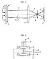
- FIG. 1 is a schematic diagram illustrating the concept of a conventional SCALPELTM system.
- a beam B of electrons 10 is directed towards a scattering mask 9 including a thin membrane 11 having a thickness between about 1,000 ⁇ and about 20,000 ⁇ (0.1 ⁇ m and about 2 ⁇ m thick.)
- the membrane 11 is composed of a material which is virtually transparent to the electron beam B composed of electrons 10. That is to say that electrons 10 in beam B pass through membrane 11 freely in the absence of any other object providing an obstruction to the path of electrons 10 in the beam B as they pass from the source of the beam through the membrane 11.
- a pattern of high density scattering elements 12 Formed on the side of the membrane 11 facing the beam 10, is a pattern of high density scattering elements 12 to provide a contrast mechanism that enables reproduction of the mask pattern at the target surface.
- the scattering elements 12 are patterned in the composite shape which is to be exposed upon a work piece 17 (usually a silicon wafer) which is coated with E-beam sensitive resist, which as shown in FIG. 1 has been processed into pattern elements 18.
- the electrons 10 from the E-beam B which pass through the mask 9 are shown by beams 14 which pass through electromagnetic lens 15 which focuses the beams 14 through an aperture 16' into an otherwise opaque back focal plane filter 16.
- the aperture 16' permits only electrons scattered at small angles to pass through to the work piece 17.
- the exposure tool 20 includes a source 22 (usually an electron gun), a mask stage 24, imaging optics 26, and a wafer stage 28.
- the mask stage 24 and the wafer stage 28 are mounted to the top and bottom of a block of aluminum, referred to as the metrology plate 30.
- the metrology plate 30, which is on the order of 3000 lbs., serves as a thermal and mechanical stabilizer for the entire exposure tool 20.
- FIG. 3 illustrates a prior art source 22 in more detail.
- the source 22 includes a cathode 42, an anode 43, a grid electrode 44, focusing plates 45, and a filament 46.
- Each of the cathode 42, anode 43, grid electrode 44, and focusing plates 45 exhibit substantial circular and radial symmetry about an imaginary line of focus 50.
- the cathode 42 is made of gallium arsenide (GaAs), bialkali cathode materials, cesium antimonide (Cs 3 Sb), or a pure material having a low work function, such as tantalum (Ta), samarium (Sm), or nickel (Ni).
- the material of photocathode 42 is made of a metal added to a semiconductor material by mixing or by depositing through sputtering or annealing.
- the metal is preferably tantalum (Ta), copper (Cu), silver (Ag), aluminum (Al), or gold (Au), or oxides or halides of these metals.
- tantalum (Ta) annealed on the surface of nickel (Ni).
- thermionic cathodes such as pure metal (tungsten or tantalum), lanthanum hexaboride (LaB 6 ), etc. cathodes are sufficient for these applications.
- thermoionic cathodes have work function variations across the emitting surface substantially greater than 2%, for example 5-10%.
- the SCALPELTM process requires a thermoionic cathode with a work function variation less than 2%.
- the conventional cathode which meets the SCALPELTM requirements for other parameters, such as emission uniformity, low work function, low evaporation rate, high voltage operating environment, and vacuum contamination resilience is a tantalum (Ta) cathode having a disk shape.
- the disk-shaped tantalum (Ta) cathode is made from cold or hot rolled tantalum (Ta) foils which are hot pressed into a micro-polycrystalline material. Because of its polycrystalline nature, the grains are substantially misoriented with each other (on the order of 5-20°).
- the conventional Ta cathode also has an uncontrolled grain size distribution between 5-400 ⁇ m.
- the conventional polycrystalline Ta cathode work function distribution is "patchy" (also on the order of 5-400 ⁇ m), varying from grain-to-grain (because of differing orientations) and resulting in an unacceptably patchy or non-uniform emission pattern.
- Patternchy also on the order of 5-400 ⁇ m
- grain-to-grain because of differing orientations
- resulting in an unacceptably patchy or non-uniform emission pattern Due to the sensitivity of tantalum's work function to the crystallographic orientation, the conventional polycrystalline Ta cathode work function distribution is "patchy" (also on the order of 5-400 ⁇ m), varying from grain-to-grain (because of differing orientations) and resulting in an unacceptably patchy or non-uniform emission pattern.
- Growth of the misoriented and differing sized grains at a high operating temperature further aggravates the patchiness problem.
- the conventional polycrystalline cathode materials When used as a SCALPELTM cathode, the conventional polycrystalline cathode materials experience grain growth and rough texture development (together termed “recrystallization") at the SCALPELTM high operating temperatures (1200-2000°C) and extended time period (greater than 1000 hours). Although the total emission current is satisfactory, structural developments at the cathode surface causes dark patches to appear on the cathode surface and make the cathode unacceptable for SCALPELTM. In addition, conventional cathode materials, such as LaB 6 , are easily contaminated by the SCALPELTM operating environment, as described in "Design of a low-brightness, highly uniform source for projection electron-beam lithography (SCALPEL)", W.K. Waskiewicz et al., Proc. SPIE, 3155 (1997).
- SCALPEL design of a low-brightness, highly uniform source for projection electron-beam lithography
- the present invention solves these problems with conventional cathodes used in SCALPELTM and similar systems by providing a cathode that has a buffer between a polycrystalline substrate and an emissive layer.
- the work function of the conventional polycrystalline substrate surface is non-uniform due to the non-uniform grain crystallography of the substrate material at the surface. These non-uniformities include grain misorientations on the order of 5-20° and grain size variations from 5-400 ⁇ m. Recrystallization over time also results in an increase in grain size and misorientation.
- the buffer alters, randomizes, miniaturizes (preferably to grain sizes less than 4 ⁇ m), and/or isolates the emissive layer, in a crystallographic sense, from the underlying substrate. The buffer also reduces the rate at which the substrate and emissive layer recrystallize over time.
- the buffer also includes a refractory metal or carbon.
- the substrate is tantalum
- the buffer is a dual layer of molybdenum and tungsten
- the emissive layer is tantalum.
- the molybdenum modifies the tantalum structure (lattice constant and orientation) in the underlying substrate by dissolving into the substrate, which reduces grain misorientation.
- the tungsten also dissolves into the substrate and, as a result of its high melting temperature, reduces the rate of recrystallization of both the underlying tantalum substrate and the overlying tantalum emissive layer.
- the buffer reduces the rate at which the substrate and emissive layer recrystallize over time by at least 30% and preferably by 50%.
- rhenium and tantalum are codeposited to form the buffer.
- the codeposit forms fine-grained (less than 4 ⁇ m) intermetallic phases and reduces subsequent recrystallization of the substrate and emissive layer.
- the codeposit does not adversely affect the electron transport from the substrate to the emissive layer, and has a coefficient of thermal expansion that approximates (within 35%, more preferably within 25%) that of the substrate and the emissive layer.
- the codeposit interacts with the substrate in a way that is different from the interaction between the substrate and the molybdenum.
- the codeposit does not dissolve and does not alter the original structure of the substrate but rather blocks and dominates the original substrate surface.
- the structure of the codeposit dominates the substrate, composed of randomly oriented fine grains of Re-Ta intermetallic phases (less than 4 ⁇ m) resulting in a uniformly distributed, averaged work function.
- the end result however, is the same; the emissive layer is effectively isolated from the substrate and not affected by the crystal structure of the substrate surface.
- the substrate is tantalum
- the buffer is rhenium
- the emissive layer is tantalum.
- the rhenium modifies the tantalum structure in the underlying substrate by reacting with the tantalum to form Re-Ta intermetallic phases, similar to those obtained with the Re-Ta codeposit and that minimizes the misorientation of the grains.
- Figure 4 illustrates a general embodiment of the method of making the cathode of the present invention.
- a surface of a substrate is prepared for deposition.
- a buffer is deposited on the substrate.
- an emissive layer is deposited on the buffer, in order to produce the cathode.
- the surface of the substrate is prepared by ion etching and vacuum annealing.
- the buffer and/or the emissive layer are deposited by magnetron sputter deposition.
- vacuum annealing is performed after deposition of both the buffer and the emissive layer.
- the buffer and layers may be deposited by a number of different methods, such as sputtering, evaporation, chemical vapor deposition (CVD), etc.
- the desired thickness of the buffer is typically in the range of 0.1 ⁇ m to 100 ⁇ m, or preferably in the range of 0.5-10 ⁇ m.
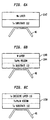
- Figure 5 illustrates a cathode of the present invention in one embodiment.
- the cathode 110 includes a substrate 112, a buffer 114, an emissive layer 116, arranged as illustrated in Figure 4.
- the buffer 114 is an altered grain structure at a surface of the substrate 112 to make the work function distribution more uniform. In another embodiment, the buffer 114 is itself a fine-grained, randomized structure that blocks the substrate 112, thereby improving the uniformity of the work function distribution of the resulting cathode 110.
- the buffer 114 alters the grain structure at the surface of the substrate by diffusion, alloying, precipitation, or new phase formation. Still further, the buffer 114 includes atoms from a chemical class similar to the chemical class of the substrate 112. For example, if the substrate 112 is a refractory metal or carbon, then the buffer 114 would also include refractory metal or carbon atoms.
- the cathode is part of a projection electron lithography system, such as the SCALPELTM system.
- the buffer 114 also provides thermal and electrical conductivities and good adhesion to withstand operating temperatures up to 2100° K.
- One additional advantage of the cathode 110 illustrated in Figure 5, is that such a layered cathode can be made in a curved shape (concave or convex), which is useful for electron beam focusing.
- Example 1 describes a first material combination that is effective in creating the desired structural uniformity and work function uniformity on the polycrystalline Ta cathode surface.
- Example 1 is a Ta/Mo/W/Ta arrangement, where Ta is the polycrystalline substrate surface, Mo/W are two sequentially applied buffer layers, and Ta is the emissive layer.
- both Mo and W have the same body centered cubic (bcc) structure as Ta, and form solid solutions. Because of the relatively small size of Mo atoms, the first buffer of Mo atoms diffuse into the Ta substrate upon annealing at 1600°C. This Mo diffusion alters the crystalline structure of the existing Ta grains. The subsequent W layer further alters the grain structure on the surface by diffusion to form a solid solution of Ta-Mo-W. The final Ta layer serves as the emissive layer because it has the lowest work function of the three.
- an Mo layer 1142 is added to the Ta substrate 112. Because of the relatively small size of the Mo atoms, the Mo atoms diffuse into the Ta substrate 112 upon annealing at 1600°C. This Mo diffusion alters or distorts the crystalline structure of the existing Ta grains to form Ta/Mo region 1144, thereby randomizing the orientation of the Ta substrate. Then, a W layer 1148 is added, as illustrated in Figure 6B . The W layer 1148 further randomizes the grain structure on the surface by diffusion to form a solid solution of Ta/Mo/W at 1150. Finally, the Ta emissive layer 116 is added, as illustrated in Figure 6C. The final Ta layer serves as the emissive layer, because it has the lowest work function of the three. The grain structure of the Ta layer 116 is also randomized because of the underlying Ta/Mo/W region 150.
- the Mo layer 1142 and W layer 1148 are typically added at a thickness of 0.5-10 ⁇ m.
- both the Mo layer 1142 and the W layer 1148 may be selected from the group including Mo, W, Nb, V, Ir, Rh, or any combination thereof.
- Example 2 describes a second material combination that is effective in creating the desired structural uniformity and work function uniformity on the polycrystalline Ta cathode surface.
- Example 2 is a Ta/Re-Ta/Ta arrangement, where Ta is the polycrystalline substrate 112, Re-Ta is an alloyed buffer film 113, and Ta is the emissive layer 116, as illustrated in Figure 7.
- Re has a hexagonal close-packed (hcp) structure, it forms various intermetallic compounds with Ta.
- the co-sputtered Re-Ta alloy film 113 thus consists of fine-grained ( ⁇ 4 ⁇ m), randomly oriented surface structure, which blocks the original polycrystalline grain structure of the Ta substrate 112.
- the subsequent emissive Ta layer 116 also has the same fine grain structure because of the Re-Ta alloy film 113. Because of the formation of intermetallic compounds and the resultant multiphase structure, the grains in the substrate 112 are largely pinned by the new phases of the buffer film 113 at the boundaries and their growth is inhibited at the operating temperature (2100°K). Also Re has a close match with Ta in its thermal expansion coefficient, and as a result, the buildup of thermal stress which cause film delamination and cracking, is reduced.
- intermetallic compound of Example 2 is a Re-Ta alloy
- other combinations are also effective including C-Ta, Hf-Ta, Os-Ta, and Ru-Ta.
- Example 3 describes a third material combination that is effective in creating the desired structural uniformity and work function uniformity on the polycrystalline Ta cathode surface.
- Example 3 is a Ta/Re/Ta arrangement, where Ta is the polycrystalline substrate 112, Re is a buffer layer 1160, and Ta is the emissive layer 116, as illustrated in Figure 8.
- a Re layer 1160 is added to the Ta substrate 112.
- the Re reacts with Ta to form Re-Ta intermetallic compounds. Similar to Example 2, these Re-Ta intermetallic compounds have a fine grained ( ⁇ 4 ⁇ m) randomly oriented surface structure, which block the original polycrystalline grain structure of the Ta substrate 112.
- the Ta emissive layer 116 is added, as illustrated in Figure 8B.
- the final Ta layer serves as the emissive layer, because it has the lowest work function of the three.
- the grain structure of the Ta layer 116 is fine and randomized because of the underlying Re-Ta alloy 1162.
- Examples 1-3 have shown improved uniform emission characteristics in emission microscopes and SCALPELTM machines compared to the conventional Ta cathode.
Landscapes
- Engineering & Computer Science (AREA)
- Manufacturing & Machinery (AREA)
- Chemical & Material Sciences (AREA)
- Analytical Chemistry (AREA)
- Electron Beam Exposure (AREA)
- Electron Sources, Ion Sources (AREA)
- Solid Thermionic Cathode (AREA)
- Cold Cathode And The Manufacture (AREA)
- Crystals, And After-Treatments Of Crystals (AREA)
Abstract
Description
- The present invention relates to a cathode for use in electron beam projection lithography and a method for making the cathode, and more particularly, to a cathode with an improved work function and a method for making the improved work function cathode.
- Projection electron beam lithography, such as Scattering Angular Limitation Projection Electron Beam Lithograph (SCALPEL™), utilizes electron beam radiation projected onto a patterned mask to transfer an image of that pattern into a layer of energy sensitive material formed on a substrate. That image is developed and used in subsequent processing to form devices such as integrated circuits.
- The SCALPEL™ mask has a membrane of a low atomic number material on which is formed a layer of high atomic number material. The layer of high atomic number material has a pattern delineated therein. Both the low atomic number membrane material and the high atomic number patterned layer of material are transparent to the electrons projected thereon (i.e., electrons with an energy of about 100 keV). However, the low atomic number membrane materials scatters the electrons weakly and at small angles. The high atomic number patterned layer of material scatters the electrons strongly and at large angles. Thus, the electrons transmitted through the high atomic number patterned material have a larger scattering angle than the electrons transmitted through the membrane. This difference in scattering angle provides a contrast between the electrons transmitted through the membrane alone and the electrons transmitted through the layer of patterned material formed on the membrane.
- This contrast is exploited to transfer an image of the pattern from the mask and into a layer of energy sensitive material by using a back focal plane filter in the projection optics between the mask and the layer of energy sensitive material. The back focal pane filter has an aperture therein. The weakly scattered electrons are transmitted through the aperture while the strongly scattered electrons are blocked by the back focal plane filter. Thus, the image of the pattern defined in the weakly scattered electrons is transmitted through the aperture and into the layer of energy sensitive material.
- FIG. 1 is a schematic diagram illustrating the concept of a conventional SCALPEL™ system. A beam B of electrons 10 is directed towards a
scattering mask 9 including athin membrane 11 having a thickness between about 1,000 Å and about 20,000 Å (0.1 µm and about 2 µm thick.) Themembrane 11 is composed of a material which is virtually transparent to the electron beam B composed of electrons 10. That is to say that electrons 10 in beam B pass throughmembrane 11 freely in the absence of any other object providing an obstruction to the path of electrons 10 in the beam B as they pass from the source of the beam through themembrane 11. - Formed on the side of the
membrane 11 facing the beam 10, is a pattern of highdensity scattering elements 12 to provide a contrast mechanism that enables reproduction of the mask pattern at the target surface. Thescattering elements 12 are patterned in the composite shape which is to be exposed upon a work piece 17 (usually a silicon wafer) which is coated with E-beam sensitive resist, which as shown in FIG. 1 has been processed intopattern elements 18. The electrons 10 from the E-beam B which pass through themask 9 are shown bybeams 14 which pass throughelectromagnetic lens 15 which focuses thebeams 14 through an aperture 16' into an otherwise opaque backfocal plane filter 16. The aperture 16' permits only electrons scattered at small angles to pass through to thework piece 17. - A conventional SCALPEL™ exposure tool is illustrated in Figure 2. The
exposure tool 20 includes a source 22 (usually an electron gun), amask stage 24,imaging optics 26, and awafer stage 28. Themask stage 24 and thewafer stage 28 are mounted to the top and bottom of a block of aluminum, referred to as themetrology plate 30. Themetrology plate 30, which is on the order of 3000 lbs., serves as a thermal and mechanical stabilizer for theentire exposure tool 20. - Figure 3 illustrates a
prior art source 22 in more detail. Thesource 22 includes acathode 42, ananode 43, agrid electrode 44, focusingplates 45, and afilament 46. Each of thecathode 42,anode 43,grid electrode 44, and focusingplates 45 exhibit substantial circular and radial symmetry about an imaginary line offocus 50. In the prior art systems in U.S. Patent No. 5,426,686, thecathode 42 is made of gallium arsenide (GaAs), bialkali cathode materials, cesium antimonide (Cs3Sb), or a pure material having a low work function, such as tantalum (Ta), samarium (Sm), or nickel (Ni). In other prior art systems disclosed in U.S. Patent No. 5,426,686, the material ofphotocathode 42 is made of a metal added to a semiconductor material by mixing or by depositing through sputtering or annealing. The metal is preferably tantalum (Ta), copper (Cu), silver (Ag), aluminum (Al), or gold (Au), or oxides or halides of these metals. One such example of a prior art photocathode is constructed from tantalum (Ta) annealed on the surface of nickel (Ni). - Most e-beam lithography systems (direct e-beam writing machines, etc.) require essentially point electron sources with high current densities. Conventional thermionic cathodes, such as pure metal (tungsten or tantalum), lanthanum hexaboride (LaB6), etc. cathodes are sufficient for these applications.
- In contrast, SCALPEL™ systems require a 1 mm2 approximately parallel electron beam with a cross-sectional current density variation of within 2%. Conventional thermoionic cathodes have work function variations across the emitting surface substantially greater than 2%, for example 5-10%. However, as noted on page 3769 of "High emittance electron gun for projection lithography," W. Devore et al., 1998 American Vacuum Society, J. Vac. Sci. Technol. B 14(6), Nov/Dec. 1996, pp. 3764-3769, the SCALPEL™ process requires a thermoionic cathode with a work function variation less than 2%.
- The conventional cathode which meets the SCALPEL™ requirements for other parameters, such as emission uniformity, low work function, low evaporation rate, high voltage operating environment, and vacuum contamination resilience is a tantalum (Ta) cathode having a disk shape. The disk-shaped tantalum (Ta) cathode is made from cold or hot rolled tantalum (Ta) foils which are hot pressed into a micro-polycrystalline material. Because of its polycrystalline nature, the grains are substantially misoriented with each other (on the order of 5-20°). The conventional Ta cathode also has an uncontrolled grain size distribution between 5-400 µm. Due to the sensitivity of tantalum's work function to the crystallographic orientation, the conventional polycrystalline Ta cathode work function distribution is "patchy" (also on the order of 5-400 µm), varying from grain-to-grain (because of differing orientations) and resulting in an unacceptably patchy or non-uniform emission pattern. Growth of the misoriented and differing sized grains at a high operating temperature further aggravates the patchiness problem. The non-uniformities caused by grain misorientation, uncontrolled large grain sizes, and grain growth on the cathode surface at the high operating temperature are transferred by the SCALPEL™ electron optics down to the shaping aperture (the object plane) and eventually to the wafer surface (the imaging plane).
- When used as a SCALPEL™ cathode, the conventional polycrystalline cathode materials experience grain growth and rough texture development (together termed "recrystallization") at the SCALPEL™ high operating temperatures (1200-2000°C) and extended time period (greater than 1000 hours). Although the total emission current is satisfactory, structural developments at the cathode surface causes dark patches to appear on the cathode surface and make the cathode unacceptable for SCALPEL™. In addition, conventional cathode materials, such as LaB6, are easily contaminated by the SCALPEL™ operating environment, as described in "Design of a low-brightness, highly uniform source for projection electron-beam lithography (SCALPEL)", W.K. Waskiewicz et al., Proc. SPIE, 3155 (1997).
- The present invention solves these problems with conventional cathodes used in SCALPEL™ and similar systems by providing a cathode that has a buffer between a polycrystalline substrate and an emissive layer.
- The work function of the conventional polycrystalline substrate surface is non-uniform due to the non-uniform grain crystallography of the substrate material at the surface. These non-uniformities include grain misorientations on the order of 5-20° and grain size variations from 5-400 µm. Recrystallization over time also results in an increase in grain size and misorientation. The buffer alters, randomizes, miniaturizes (preferably to grain sizes less than 4 µm), and/or isolates the emissive layer, in a crystallographic sense, from the underlying substrate. The buffer also reduces the rate at which the substrate and emissive layer recrystallize over time.
- In an example where the cathode is a refractory metal or carbon cathode (e.g., a tantalum cathode) the buffer also includes a refractory metal or carbon.
- In one example, the substrate is tantalum, the buffer is a dual layer of molybdenum and tungsten, and the emissive layer is tantalum. The molybdenum modifies the tantalum structure (lattice constant and orientation) in the underlying substrate by dissolving into the substrate, which reduces grain misorientation. The tungsten also dissolves into the substrate and, as a result of its high melting temperature, reduces the rate of recrystallization of both the underlying tantalum substrate and the overlying tantalum emissive layer. In particular, the buffer reduces the rate at which the substrate and emissive layer recrystallize over time by at least 30% and preferably by 50%.
- In another example, rhenium and tantalum are codeposited to form the buffer. The codeposit forms fine-grained (less than 4 µm) intermetallic phases and reduces subsequent recrystallization of the substrate and emissive layer. The codeposit does not adversely affect the electron transport from the substrate to the emissive layer, and has a coefficient of thermal expansion that approximates (within 35%, more preferably within 25%) that of the substrate and the emissive layer.
- However, the codeposit interacts with the substrate in a way that is different from the interaction between the substrate and the molybdenum. The codeposit does not dissolve and does not alter the original structure of the substrate but rather blocks and dominates the original substrate surface. In effect, the structure of the codeposit dominates the substrate, composed of randomly oriented fine grains of Re-Ta intermetallic phases (less than 4 µm) resulting in a uniformly distributed, averaged work function. The end result however, is the same; the emissive layer is effectively isolated from the substrate and not affected by the crystal structure of the substrate surface.
- In another example, the substrate is tantalum, the buffer is rhenium, and the emissive layer is tantalum. The rhenium modifies the tantalum structure in the underlying substrate by reacting with the tantalum to form Re-Ta intermetallic phases, similar to those obtained with the Re-Ta codeposit and that minimizes the misorientation of the grains.
-
- Figure 1 is a schematic diagram illustrating the concept of a SCALPEL™ (Scattering Angle Limited Projection E-beam Lithography) system.
- Figure 2 illustrates a conventional SCALPEL™ exposure tool.
- Figure 3 illustrates a conventional source for the SCALPEL™ system of Figure 1.
- Figure 4 illustrates a general method of making the cathode of the present invention.
- Figure 5 illustrates the general cathode of the present invention.
- Figures 6A-6C illustrate a cathode with a solid solution buffer region.
- Figure 7 illustrates a cathode with an alloy buffer film.
- Figure 8A-8B illustrate another cathode with a solid solution buffer region.
-
- Figure 4 illustrates a general embodiment of the method of making the cathode of the present invention. As illustrated in Figure 4, in
step 100, a surface of a substrate is prepared for deposition. Instep 200, a buffer is deposited on the substrate. Instep 300, an emissive layer is deposited on the buffer, in order to produce the cathode. - In more particular embodiments, the surface of the substrate is prepared by ion etching and vacuum annealing. Further, the buffer and/or the emissive layer are deposited by magnetron sputter deposition. Further, in preferred embodiments, vacuum annealing is performed after deposition of both the buffer and the emissive layer.
- In other preferred embodiments, the buffer and layers may be deposited by a number of different methods, such as sputtering, evaporation, chemical vapor deposition (CVD), etc. The desired thickness of the buffer is typically in the range of 0.1 µm to 100 µm, or preferably in the range of 0.5-10 µm.
- Figure 5 illustrates a cathode of the present invention in one embodiment. In particular, Figure 5 illustrates that the
cathode 110 includes asubstrate 112, a buffer 114, anemissive layer 116, arranged as illustrated in Figure 4. - In one embodiment, the buffer 114 is an altered grain structure at a surface of the
substrate 112 to make the work function distribution more uniform. In another embodiment, the buffer 114 is itself a fine-grained, randomized structure that blocks thesubstrate 112, thereby improving the uniformity of the work function distribution of the resultingcathode 110. - In more particular embodiments of the present invention, the buffer 114 alters the grain structure at the surface of the substrate by diffusion, alloying, precipitation, or new phase formation. Still further, the buffer 114 includes atoms from a chemical class similar to the chemical class of the
substrate 112. For example, if thesubstrate 112 is a refractory metal or carbon, then the buffer 114 would also include refractory metal or carbon atoms. In another preferred embodiment, the cathode is part of a projection electron lithography system, such as the SCALPEL™ system. - The buffer 114 also provides thermal and electrical conductivities and good adhesion to withstand operating temperatures up to 2100° K. One additional advantage of the
cathode 110 illustrated in Figure 5, is that such a layered cathode can be made in a curved shape (concave or convex), which is useful for electron beam focusing. - Example 1 describes a first material combination that is effective in creating the desired structural uniformity and work function uniformity on the polycrystalline Ta cathode surface. Example 1 is a Ta/Mo/W/Ta arrangement, where Ta is the polycrystalline substrate surface, Mo/W are two sequentially applied buffer layers, and Ta is the emissive layer.
- In the Ta/Mo/W/Ta system, both Mo and W have the same body centered cubic (bcc) structure as Ta, and form solid solutions. Because of the relatively small size of Mo atoms, the first buffer of Mo atoms diffuse into the Ta substrate upon annealing at 1600°C. This Mo diffusion alters the crystalline structure of the existing Ta grains. The subsequent W layer further alters the grain structure on the surface by diffusion to form a solid solution of Ta-Mo-W. The final Ta layer serves as the emissive layer because it has the lowest work function of the three.
- In Figure 6A, an
Mo layer 1142 is added to theTa substrate 112. Because of the relatively small size of the Mo atoms, the Mo atoms diffuse into theTa substrate 112 upon annealing at 1600°C. This Mo diffusion alters or distorts the crystalline structure of the existing Ta grains to form Ta/Mo region 1144, thereby randomizing the orientation of the Ta substrate. Then, aW layer 1148 is added, as illustrated in Figure 6B . TheW layer 1148 further randomizes the grain structure on the surface by diffusion to form a solid solution of Ta/Mo/W at 1150. Finally, the Taemissive layer 116 is added, as illustrated in Figure 6C. The final Ta layer serves as the emissive layer, because it has the lowest work function of the three. The grain structure of theTa layer 116 is also randomized because of the underlying Ta/Mo/W region 150. - The
Mo layer 1142 andW layer 1148 are typically added at a thickness of 0.5-10 µm. In other preferred examples, both theMo layer 1142 and theW layer 1148 may be selected from the group including Mo, W, Nb, V, Ir, Rh, or any combination thereof. - Example 2 describes a second material combination that is effective in creating the desired structural uniformity and work function uniformity on the polycrystalline Ta cathode surface. Example 2 is a Ta/Re-Ta/Ta arrangement, where Ta is the
polycrystalline substrate 112, Re-Ta is an alloyedbuffer film 113, and Ta is theemissive layer 116, as illustrated in Figure 7. - Because Re has a hexagonal close-packed (hcp) structure, it forms various intermetallic compounds with Ta. The co-sputtered
Re-Ta alloy film 113 thus consists of fine-grained (<4 µm), randomly oriented surface structure, which blocks the original polycrystalline grain structure of theTa substrate 112. The subsequentemissive Ta layer 116 also has the same fine grain structure because of theRe-Ta alloy film 113. Because of the formation of intermetallic compounds and the resultant multiphase structure, the grains in thesubstrate 112 are largely pinned by the new phases of thebuffer film 113 at the boundaries and their growth is inhibited at the operating temperature (2100°K). Also Re has a close match with Ta in its thermal expansion coefficient, and as a result, the buildup of thermal stress which cause film delamination and cracking, is reduced. - Although the intermetallic compound of Example 2 is a Re-Ta alloy, other combinations are also effective including C-Ta, Hf-Ta, Os-Ta, and Ru-Ta.
- Example 3 describes a third material combination that is effective in creating the desired structural uniformity and work function uniformity on the polycrystalline Ta cathode surface. Example 3 is a Ta/Re/Ta arrangement, where Ta is the
polycrystalline substrate 112, Re is abuffer layer 1160, and Ta is theemissive layer 116, as illustrated in Figure 8. - In Figure 8A, a
Re layer 1160 is added to theTa substrate 112. The Re reacts with Ta to form Re-Ta intermetallic compounds. Similar to Example 2, these Re-Ta intermetallic compounds have a fine grained (<4 µm) randomly oriented surface structure, which block the original polycrystalline grain structure of theTa substrate 112. Finally, the Taemissive layer 116 is added, as illustrated in Figure 8B. The final Ta layer serves as the emissive layer, because it has the lowest work function of the three. The grain structure of theTa layer 116 is fine and randomized because of the underlyingRe-Ta alloy 1162. - The material arrangements in Examples 1-3 have shown improved uniform emission characteristics in emission microscopes and SCALPEL™ machines compared to the conventional Ta cathode.
- The invention being thus described, it will be obvious that the same may be varied in many ways. Such variations are not to be regarded as a departure from the scope of the invention.
Claims (35)
- A thermoionic cathode, comprising:a substrate;an emissive layer; anda buffer, located between said substrate and said emissive layer, said buffer modifying a grain structure at a surface of said substrate contacting said buffer.
- The thermoionic cathode of claim 1, said buffer further randomizing a crystallographic orientation of the grain structure at a surface of said substrate contacting said buffer.
- The thermoionic cathode of claim 1, said buffer further miniaturizing grain sizes of grains at the surface of said substrate contacting said buffer.
- The thermoionic cathode of claim 3, wherein the grain sizes of the grains at the surface of said substrate are less than 4 µm.
- The thermoionic cathode of claim 1, wherein said buffer modifies the grain structure at the surface of said substrate contacting said buffer by one of altering and blocking.
- The thermoionic cathode of claim 5, said buffer altering the grain structure at the surface of said substrate contacting said buffer by at least one of dissolution, alloying, reaction, precipitation, and new phase formation.
- The thermoionic cathode of claim 1, wherein said buffer is from a chemical class similar to a chemical class of said substrate.
- The thermoionic cathode of claim 7, wherein said buffer and said substrate are both refractory metals or carbon.
- The thermoionic cathode of claim 1, wherein said cathode has a curved shape.
- The thermoionic cathode of claim 6, wherein said buffer is a solid solution buffer.
- The thermoionic cathode of claim 10, wherein said buffer includes at least two of the group consisting of Mo, W, Nb, V, Ir, Rh, and Ta.
- The thermoionic cathode of claim 11, wherein the solid solution buffer includes molybdenum, tungsten and tantalum.
- The thermoionic cathode of claim 12, wherein said substrate and said emissive layer are made of tantalum.
- The thermoionic cathode of claim 1, wherein said cathode is part of a projection electron lithography system.
- The thermoionic cathode of claim 14, wherein the projection electron lithography system is a SCALPEL™ system.
- The thermoionic cathode of claim 5, said buffer blocking the grain structure at the surface of said substrate contacting said buffer by at least one of alloying, reaction, precipitation, and new phase formation.
- The thermoionic cathode of claim 16, wherein said buffer is an alloyed buffer.
- The thermoionic cathode of claim 17, wherein said buffer is an alloy comprising at least two elements with different crystalline structure.
- The thermoionic cathode of claim 17, wherein said buffer is made of a grain growth inhibiting multiphase structure.
- The thermoionic cathode of claim 16, wherein said buffer includes at least two of Re, Ta, C, Hf Tc, Os, and Ru.
- The thermoionic cathode of claim 20, wherein the buffer includes rhenium and tantalum.
- The thermoionic cathode of claim 21, wherein said substrate and said emissive layer are made of tantalum.
- A method of making a thermoionic cathode, comprising:preparing a surface of a substrate;depositing a buffer on the substrate, wherein the buffer modifies a grain structure at the surface of the substrate contacting the buffer;depositing an emissive layer on the buffer.
- The method of making the thermoionic cathode of claim 23, said step of preparing the surface of the substrate including the steps of,ion etching and vacuum annealing the surface of the substrate.
- The method of making the thermoionic cathode of claim 23, wherein the buffer is deposited by sputtering.
- The method of making the thermoionic cathode of claim 23, wherein the emissive layer is deposited by sputtering.
- The method of making the thermoionic cathode of claim 23, further comprising:vacuum annealing the buffer, after deposition of the buffer; andvacuum annealing the emissive layer, after deposition of the emissive layer.
- The method of claim 23, said buffer further randomizing a crystallographic orientation of the grain structure at the surface of the substrate contacting the buffer.
- The method of claim 23, said buffer further miniaturizing grain sizes of grains at the surface of said substrate contacting said buffer.
- The method of claim 29, wherein the grain sizes of the grains at the surface of said substrate are less than 4 µm.
- The method of claim 23, wherein said buffer modifies the grain structure at the surface of said substrate contacting said buffer by one of altering and blocking.
- The method of claim 31, wherein the buffer alters the grain structure at the surface of the substrate contacting the buffer by at least one of diffusion, alloying, reaction, precipitation, and new phase formation.
- The method of claim 32, wherein the buffer is deposited by co-sputtering Ta and at least one of Re, C, Hf, Os, and Ru on the substrate.
- The method of claim 31, said buffer blocking the grain structure at the surface of said substrate contacting said buffer by at least one of alloying, reaction, precipitation, and new phase formation.
- The method of claim 33, wherein the buffer is deposited by sputtering at least one of Re, C, Hf, Os, and Ru on the substrate.
Applications Claiming Priority (2)
| Application Number | Priority Date | Filing Date | Title |
|---|---|---|---|
| US338520 | 1999-06-23 | ||
| US09/338,520 US6815876B1 (en) | 1999-06-23 | 1999-06-23 | Cathode with improved work function and method for making the same |
Publications (3)
| Publication Number | Publication Date |
|---|---|
| EP1063669A2 true EP1063669A2 (en) | 2000-12-27 |
| EP1063669A3 EP1063669A3 (en) | 2006-08-16 |
| EP1063669B1 EP1063669B1 (en) | 2010-04-14 |
Family
ID=23325134
Family Applications (1)
| Application Number | Title | Priority Date | Filing Date |
|---|---|---|---|
| EP00305015A Expired - Lifetime EP1063669B1 (en) | 1999-06-23 | 2000-06-13 | Cathode with improved work function and method for making the same |
Country Status (6)
| Country | Link |
|---|---|
| US (2) | US6815876B1 (en) |
| EP (1) | EP1063669B1 (en) |
| JP (1) | JP3901915B2 (en) |
| KR (1) | KR100744896B1 (en) |
| DE (1) | DE60044167D1 (en) |
| TW (1) | TW454216B (en) |
Cited By (2)
| Publication number | Priority date | Publication date | Assignee | Title |
|---|---|---|---|---|
| DE102008020187A1 (en) * | 2008-04-22 | 2009-10-29 | Siemens Aktiengesellschaft | Cathode, has flat emitter emitting electrons, and emission layer with circular cross section arranged on emitter, where material of emission layer has lower emission function than that of material of emitter |
| DE102008020165A1 (en) * | 2008-04-22 | 2009-10-29 | Siemens Aktiengesellschaft | Cathode, has emitter made of material and emitting electrons thermally, and emission layer made of material and partially applied on emitter, where material of emission layer exhibits electron work function less than material of emitter |
Citations (6)
| Publication number | Priority date | Publication date | Assignee | Title |
|---|---|---|---|---|
| GB1070473A (en) * | 1963-06-03 | 1967-06-01 | Varian Associates | Thermionic emitter for electron discharge devices and methods of fabricating same |
| US4168565A (en) * | 1977-05-18 | 1979-09-25 | Denki Kagaku Kogyo Kabushiki Kaisha | Method for manufacturing thermionic cathode |
| US4274030A (en) * | 1978-05-05 | 1981-06-16 | Bbc Brown, Boveri & Company, Limited | Thermionic cathode |
| JPS57128436A (en) * | 1981-02-02 | 1982-08-10 | Koichi Kanetani | Manufacture of lanthanum-boride thermionic emission electrode |
| JPH0757617A (en) * | 1993-08-12 | 1995-03-03 | Ricoh Opt Ind Co Ltd | Thermal electron generation source |
| EP0845797A2 (en) * | 1996-11-29 | 1998-06-03 | Mitsubishi Denki Kabushiki Kaisha | Electron tube cathode |
Family Cites Families (13)
| Publication number | Priority date | Publication date | Assignee | Title |
|---|---|---|---|---|
| US3488549A (en) * | 1968-01-15 | 1970-01-06 | Gen Electric | Dispenser cathode material and method of manufacture |
| CH582951A5 (en) * | 1973-07-09 | 1976-12-15 | Bbc Brown Boveri & Cie | |
| US4184100A (en) * | 1977-03-29 | 1980-01-15 | Tokyo Shibaura Electric Co., Ltd. | Indirectly-heated cathode device for electron tubes |
| US4272030A (en) * | 1979-07-30 | 1981-06-09 | Afanasiev Mikhail M | Device for adjusting an inertia cone crusher discharge gap |
| JPS57196443A (en) * | 1981-05-29 | 1982-12-02 | Denki Kagaku Kogyo Kk | Manufacture of hot cathode |
| DE3148441A1 (en) * | 1981-12-08 | 1983-07-21 | Philips Patentverwaltung Gmbh, 2000 Hamburg | METHOD FOR PRODUCING A THERMIONIC CATHODE |
| DE3205746A1 (en) * | 1982-02-18 | 1983-08-25 | Philips Patentverwaltung Gmbh, 2000 Hamburg | THERMIONIC CATHODE AND METHOD FOR THE PRODUCTION THEREOF |
| US4528452A (en) * | 1982-12-09 | 1985-07-09 | Electron Beam Corporation | Alignment and detection system for electron image projectors |
| JPS62213031A (en) * | 1986-03-14 | 1987-09-18 | Hitachi Ltd | Impregnated type cathode structure |
| US5042058A (en) | 1989-03-22 | 1991-08-20 | University Of California | Ultrashort time-resolved x-ray source |
| JP2937145B2 (en) * | 1996-10-25 | 1999-08-23 | 三菱電機株式会社 | Cathode for electron tube |
| US5911919A (en) * | 1997-09-08 | 1999-06-15 | Integrated Thermal Sciences, Inc. | Electron emission materials and components |
| EP1046184B1 (en) * | 1998-09-09 | 2003-12-03 | Koninklijke Philips Electronics N.V. | Quadrupole device for projection lithography by means of charged particles |
-
1999
- 1999-06-23 US US09/338,520 patent/US6815876B1/en not_active Expired - Fee Related
-
2000
- 2000-06-13 DE DE60044167T patent/DE60044167D1/en not_active Expired - Lifetime
- 2000-06-13 EP EP00305015A patent/EP1063669B1/en not_active Expired - Lifetime
- 2000-06-19 TW TW089111997A patent/TW454216B/en not_active IP Right Cessation
- 2000-06-22 KR KR1020000034530A patent/KR100744896B1/en not_active IP Right Cessation
- 2000-06-23 JP JP2000188555A patent/JP3901915B2/en not_active Expired - Fee Related
-
2004
- 2004-10-12 US US10/963,156 patent/US7179148B2/en not_active Expired - Lifetime
Patent Citations (6)
| Publication number | Priority date | Publication date | Assignee | Title |
|---|---|---|---|---|
| GB1070473A (en) * | 1963-06-03 | 1967-06-01 | Varian Associates | Thermionic emitter for electron discharge devices and methods of fabricating same |
| US4168565A (en) * | 1977-05-18 | 1979-09-25 | Denki Kagaku Kogyo Kabushiki Kaisha | Method for manufacturing thermionic cathode |
| US4274030A (en) * | 1978-05-05 | 1981-06-16 | Bbc Brown, Boveri & Company, Limited | Thermionic cathode |
| JPS57128436A (en) * | 1981-02-02 | 1982-08-10 | Koichi Kanetani | Manufacture of lanthanum-boride thermionic emission electrode |
| JPH0757617A (en) * | 1993-08-12 | 1995-03-03 | Ricoh Opt Ind Co Ltd | Thermal electron generation source |
| EP0845797A2 (en) * | 1996-11-29 | 1998-06-03 | Mitsubishi Denki Kabushiki Kaisha | Electron tube cathode |
Non-Patent Citations (4)
| Title |
|---|
| DEVORE W ET AL: "HIGH EMITTANCE ELECTRON GUN FOR PROJECTION LITHOGRAPHY" JOURNAL OF VACUUM SCIENCE AND TECHNOLOGY: PART B, AVS / AIP, MELVILLE, NEW YORK, NY, US, vol. 14, no. 6, November 1996 (1996-11), pages 3764-3769, XP000721109 ISSN: 1071-1023 * |
| HITCHNER JE; HU TC: "Polishing of Nickel Iron by Reactive Ion Etching. April 1978." IBM TECHNICAL DISCLOSURE BULLETIN, vol. 20, no. 11A, 1 April 1978 (1978-04-01), page 4560, XP002374254 New York, US * |
| HOMMA T; KHOI N N; SMELTZER W W; EMBURY J D: "The influence of surface preparation on the structures of nickel oxide formed on the (100) face of nickel" OXIDATION OF METALS, vol. 3, no. 5, September 1971 (1971-09), pages 463-473, XP009064249 Netherlands * |
| PATENT ABSTRACTS OF JAPAN vol. 006, no. 226 (E-141), 11 November 1982 (1982-11-11) -& JP 57 128436 A (KOUICHI KANETANI; others: 01), 10 August 1982 (1982-08-10) * |
Cited By (2)
| Publication number | Priority date | Publication date | Assignee | Title |
|---|---|---|---|---|
| DE102008020187A1 (en) * | 2008-04-22 | 2009-10-29 | Siemens Aktiengesellschaft | Cathode, has flat emitter emitting electrons, and emission layer with circular cross section arranged on emitter, where material of emission layer has lower emission function than that of material of emitter |
| DE102008020165A1 (en) * | 2008-04-22 | 2009-10-29 | Siemens Aktiengesellschaft | Cathode, has emitter made of material and emitting electrons thermally, and emission layer made of material and partially applied on emitter, where material of emission layer exhibits electron work function less than material of emitter |
Also Published As
| Publication number | Publication date |
|---|---|
| KR20010029829A (en) | 2001-04-16 |
| JP3901915B2 (en) | 2007-04-04 |
| KR100744896B1 (en) | 2007-08-01 |
| DE60044167D1 (en) | 2010-05-27 |
| JP2001052595A (en) | 2001-02-23 |
| EP1063669A3 (en) | 2006-08-16 |
| US20050046326A1 (en) | 2005-03-03 |
| TW454216B (en) | 2001-09-11 |
| US6815876B1 (en) | 2004-11-09 |
| US7179148B2 (en) | 2007-02-20 |
| EP1063669B1 (en) | 2010-04-14 |
Similar Documents
| Publication | Publication Date | Title |
|---|---|---|
| US5861707A (en) | Field emitter with wide band gap emission areas and method of using | |
| JPH0673476A (en) | Alloy used for electrical contact of semiconductor substrate | |
| JPS6255931A (en) | Formation of metal silicide contact and sputtering apparatustherefor | |
| EP0845797A2 (en) | Electron tube cathode | |
| US7567379B2 (en) | Technique to prevent tin contamination of mirrors and electrodes in an EUV lithography system | |
| Melngailis | Focused ion beam induced deposition: A review | |
| US7179148B2 (en) | Cathode with improved work function and method for making the same | |
| Stirland | Some observations on the structure of gold deposits on rocksalt substrates | |
| JP2000504487A (en) | Anti-reflection coating and laminated wiring line | |
| EP3336875A1 (en) | Semiconductor x-ray target | |
| US6448569B1 (en) | Bonded article having improved crystalline structure and work function uniformity and method for making the same | |
| US5118952A (en) | Patterned photo cathode and its fabrication method for electron image projection | |
| US20070144892A1 (en) | Method for forming metal film or stacked layer including metal film with reduced surface roughness | |
| Singh et al. | An x-ray spectromicroscopic study of the local structure of patterned titanium silicide | |
| Taga et al. | Sputtering and secondary ion yields of metals subjected to oxygen ion bombardment | |
| Nason et al. | Room‐temperature epitaxial growth of Ag (110)/GaAs (100) films | |
| JPH0770456B2 (en) | Method for manufacturing semiconductor device | |
| US5886459A (en) | Enhanced field emission from microtip structures | |
| Kearney et al. | Boron-based multilayers for soft x-ray optics | |
| US20230069583A1 (en) | Pellicle for an euv lithography mask and a method of manufacturing thereof | |
| JPH05140728A (en) | Apparatus for producing thin film | |
| JPH0790564A (en) | High-purity titanium sputtering target | |
| KR100215218B1 (en) | Manufacturing method of field emitter metal tip using ion transformation method | |
| JPH0291933A (en) | Ion implantation device | |
| US20090120785A1 (en) | Method for forming metal film or stacked layer including metal film with reduced surface roughness |
Legal Events
| Date | Code | Title | Description |
|---|---|---|---|
| PUAI | Public reference made under article 153(3) epc to a published international application that has entered the european phase |
Free format text: ORIGINAL CODE: 0009012 |
|
| AK | Designated contracting states |
Kind code of ref document: A2 Designated state(s): AT BE CH CY DE DK ES FI FR GB GR IE IT LI LU MC NL PT SE |
|
| AX | Request for extension of the european patent |
Free format text: AL;LT;LV;MK;RO;SI |
|
| PUAL | Search report despatched |
Free format text: ORIGINAL CODE: 0009013 |
|
| AK | Designated contracting states |
Kind code of ref document: A3 Designated state(s): AT BE CH CY DE DK ES FI FR GB GR IE IT LI LU MC NL PT SE |
|
| AX | Request for extension of the european patent |
Extension state: AL LT LV MK RO SI |
|
| 17P | Request for examination filed |
Effective date: 20061124 |
|
| 17Q | First examination report despatched |
Effective date: 20061222 |
|
| AKX | Designation fees paid |
Designated state(s): DE FR GB |
|
| RAP3 | Party data changed (applicant data changed or rights of an application transferred) |
Owner name: LUCENT TECHNOLOGIES INC. |
|
| GRAP | Despatch of communication of intention to grant a patent |
Free format text: ORIGINAL CODE: EPIDOSNIGR1 |
|
| GRAS | Grant fee paid |
Free format text: ORIGINAL CODE: EPIDOSNIGR3 |
|
| GRAA | (expected) grant |
Free format text: ORIGINAL CODE: 0009210 |
|
| AK | Designated contracting states |
Kind code of ref document: B1 Designated state(s): DE FR GB |
|
| REG | Reference to a national code |
Ref country code: GB Ref legal event code: FG4D |
|
| REF | Corresponds to: |
Ref document number: 60044167 Country of ref document: DE Date of ref document: 20100527 Kind code of ref document: P |
|
| PLBE | No opposition filed within time limit |
Free format text: ORIGINAL CODE: 0009261 |
|
| STAA | Information on the status of an ep patent application or granted ep patent |
Free format text: STATUS: NO OPPOSITION FILED WITHIN TIME LIMIT |
|
| 26N | No opposition filed |
Effective date: 20110117 |
|
| PGFP | Annual fee paid to national office [announced via postgrant information from national office to epo] |
Ref country code: FR Payment date: 20140609 Year of fee payment: 15 |
|
| PGFP | Annual fee paid to national office [announced via postgrant information from national office to epo] |
Ref country code: GB Payment date: 20150527 Year of fee payment: 16 |
|
| REG | Reference to a national code |
Ref country code: FR Ref legal event code: ST Effective date: 20160229 |
|
| PG25 | Lapsed in a contracting state [announced via postgrant information from national office to epo] |
Ref country code: FR Free format text: LAPSE BECAUSE OF NON-PAYMENT OF DUE FEES Effective date: 20150630 |
|
| GBPC | Gb: european patent ceased through non-payment of renewal fee |
Effective date: 20160613 |
|
| PG25 | Lapsed in a contracting state [announced via postgrant information from national office to epo] |
Ref country code: GB Free format text: LAPSE BECAUSE OF NON-PAYMENT OF DUE FEES Effective date: 20160613 |
|
| PGFP | Annual fee paid to national office [announced via postgrant information from national office to epo] |
Ref country code: DE Payment date: 20170522 Year of fee payment: 18 |
|
| REG | Reference to a national code |
Ref country code: DE Ref legal event code: R082 Ref document number: 60044167 Country of ref document: DE Representative=s name: DILG HAEUSLER SCHINDELMANN PATENTANWALTSGESELL, DE Ref country code: DE Ref legal event code: R081 Ref document number: 60044167 Country of ref document: DE Owner name: AVAGO TECHNOLOGIES GENERAL IP (SINGAPORE) PTE., SG Free format text: FORMER OWNER: LUCENT TECHNOLOGIES INC., MURRAY HILL, N.J., US |
|
| REG | Reference to a national code |
Ref country code: DE Ref legal event code: R119 Ref document number: 60044167 Country of ref document: DE |
|
| PG25 | Lapsed in a contracting state [announced via postgrant information from national office to epo] |
Ref country code: DE Free format text: LAPSE BECAUSE OF NON-PAYMENT OF DUE FEES Effective date: 20190101 |