EP1063240A2 - Improved organocopper precursor blend and method of depositing copper by chemical vapor deposition - Google Patents
Improved organocopper precursor blend and method of depositing copper by chemical vapor deposition Download PDFInfo
- Publication number
- EP1063240A2 EP1063240A2 EP00304591A EP00304591A EP1063240A2 EP 1063240 A2 EP1063240 A2 EP 1063240A2 EP 00304591 A EP00304591 A EP 00304591A EP 00304591 A EP00304591 A EP 00304591A EP 1063240 A2 EP1063240 A2 EP 1063240A2
- Authority
- EP
- European Patent Office
- Prior art keywords
- blend
- copper
- precursor
- weight
- percent
- Prior art date
- Legal status (The legal status is an assumption and is not a legal conclusion. Google has not performed a legal analysis and makes no representation as to the accuracy of the status listed.)
- Withdrawn
Links
- 239000010949 copper Substances 0.000 title claims abstract description 58
- 239000000203 mixture Substances 0.000 title claims abstract description 58
- RYGMFSIKBFXOCR-UHFFFAOYSA-N Copper Chemical compound [Cu] RYGMFSIKBFXOCR-UHFFFAOYSA-N 0.000 title claims abstract description 56
- 229910052802 copper Inorganic materials 0.000 title claims abstract description 56
- 239000002243 precursor Substances 0.000 title claims abstract description 21
- 238000005229 chemical vapour deposition Methods 0.000 title claims abstract description 8
- 238000000151 deposition Methods 0.000 title claims description 23
- 238000000034 method Methods 0.000 title claims description 14
- 239000006200 vaporizer Substances 0.000 claims abstract description 18
- XLYOFNOQVPJJNP-UHFFFAOYSA-N water Chemical compound O XLYOFNOQVPJJNP-UHFFFAOYSA-N 0.000 claims abstract description 13
- GCSJLQSCSDMKTP-UHFFFAOYSA-N ethenyl(trimethyl)silane Chemical compound C[Si](C)(C)C=C GCSJLQSCSDMKTP-UHFFFAOYSA-N 0.000 claims abstract 8
- 239000012691 Cu precursor Substances 0.000 claims description 16
- 239000000758 substrate Substances 0.000 claims description 5
- 230000008016 vaporization Effects 0.000 claims 1
- 230000008021 deposition Effects 0.000 description 17
- 238000002310 reflectometry Methods 0.000 description 7
- 235000012431 wafers Nutrition 0.000 description 5
- 229910052782 aluminium Inorganic materials 0.000 description 3
- XAGFODPZIPBFFR-UHFFFAOYSA-N aluminium Chemical compound [Al] XAGFODPZIPBFFR-UHFFFAOYSA-N 0.000 description 3
- 238000000354 decomposition reaction Methods 0.000 description 3
- 229910052751 metal Inorganic materials 0.000 description 3
- 239000002184 metal Substances 0.000 description 3
- 239000002245 particle Substances 0.000 description 3
- 238000012545 processing Methods 0.000 description 3
- XNMQEEKYCVKGBD-UHFFFAOYSA-N 2-butyne Chemical compound CC#CC XNMQEEKYCVKGBD-UHFFFAOYSA-N 0.000 description 2
- ATJFFYVFTNAWJD-UHFFFAOYSA-N Tin Chemical compound [Sn] ATJFFYVFTNAWJD-UHFFFAOYSA-N 0.000 description 2
- 230000004888 barrier function Effects 0.000 description 2
- 238000013461 design Methods 0.000 description 2
- 238000010586 diagram Methods 0.000 description 2
- 150000004683 dihydrates Chemical group 0.000 description 2
- 239000007789 gas Substances 0.000 description 2
- 239000012535 impurity Substances 0.000 description 2
- 239000004615 ingredient Substances 0.000 description 2
- 239000000463 material Substances 0.000 description 2
- 239000000126 substance Substances 0.000 description 2
- 230000004584 weight gain Effects 0.000 description 2
- 235000019786 weight gain Nutrition 0.000 description 2
- 239000000654 additive Substances 0.000 description 1
- 230000015572 biosynthetic process Effects 0.000 description 1
- 239000006227 byproduct Substances 0.000 description 1
- 238000010960 commercial process Methods 0.000 description 1
- 238000011109 contamination Methods 0.000 description 1
- 238000007323 disproportionation reaction Methods 0.000 description 1
- 239000007788 liquid Substances 0.000 description 1
- 238000004519 manufacturing process Methods 0.000 description 1
- 238000002156 mixing Methods 0.000 description 1
- 239000000843 powder Substances 0.000 description 1
- 238000011160 research Methods 0.000 description 1
- 239000004065 semiconductor Substances 0.000 description 1
- 230000035945 sensitivity Effects 0.000 description 1
- 229910052710 silicon Inorganic materials 0.000 description 1
- 239000010703 silicon Substances 0.000 description 1
- 238000012360 testing method Methods 0.000 description 1
Images

Classifications
-
- C—CHEMISTRY; METALLURGY
- C23—COATING METALLIC MATERIAL; COATING MATERIAL WITH METALLIC MATERIAL; CHEMICAL SURFACE TREATMENT; DIFFUSION TREATMENT OF METALLIC MATERIAL; COATING BY VACUUM EVAPORATION, BY SPUTTERING, BY ION IMPLANTATION OR BY CHEMICAL VAPOUR DEPOSITION, IN GENERAL; INHIBITING CORROSION OF METALLIC MATERIAL OR INCRUSTATION IN GENERAL
- C23C—COATING METALLIC MATERIAL; COATING MATERIAL WITH METALLIC MATERIAL; SURFACE TREATMENT OF METALLIC MATERIAL BY DIFFUSION INTO THE SURFACE, BY CHEMICAL CONVERSION OR SUBSTITUTION; COATING BY VACUUM EVAPORATION, BY SPUTTERING, BY ION IMPLANTATION OR BY CHEMICAL VAPOUR DEPOSITION, IN GENERAL
- C23C16/00—Chemical coating by decomposition of gaseous compounds, without leaving reaction products of surface material in the coating, i.e. chemical vapour deposition [CVD] processes
- C23C16/06—Chemical coating by decomposition of gaseous compounds, without leaving reaction products of surface material in the coating, i.e. chemical vapour deposition [CVD] processes characterised by the deposition of metallic material
- C23C16/18—Chemical coating by decomposition of gaseous compounds, without leaving reaction products of surface material in the coating, i.e. chemical vapour deposition [CVD] processes characterised by the deposition of metallic material from metallo-organic compounds
-
- C—CHEMISTRY; METALLURGY
- C23—COATING METALLIC MATERIAL; COATING MATERIAL WITH METALLIC MATERIAL; CHEMICAL SURFACE TREATMENT; DIFFUSION TREATMENT OF METALLIC MATERIAL; COATING BY VACUUM EVAPORATION, BY SPUTTERING, BY ION IMPLANTATION OR BY CHEMICAL VAPOUR DEPOSITION, IN GENERAL; INHIBITING CORROSION OF METALLIC MATERIAL OR INCRUSTATION IN GENERAL
- C23C—COATING METALLIC MATERIAL; COATING MATERIAL WITH METALLIC MATERIAL; SURFACE TREATMENT OF METALLIC MATERIAL BY DIFFUSION INTO THE SURFACE, BY CHEMICAL CONVERSION OR SUBSTITUTION; COATING BY VACUUM EVAPORATION, BY SPUTTERING, BY ION IMPLANTATION OR BY CHEMICAL VAPOUR DEPOSITION, IN GENERAL
- C23C16/00—Chemical coating by decomposition of gaseous compounds, without leaving reaction products of surface material in the coating, i.e. chemical vapour deposition [CVD] processes
- C23C16/44—Chemical coating by decomposition of gaseous compounds, without leaving reaction products of surface material in the coating, i.e. chemical vapour deposition [CVD] processes characterised by the method of coating
- C23C16/448—Chemical coating by decomposition of gaseous compounds, without leaving reaction products of surface material in the coating, i.e. chemical vapour deposition [CVD] processes characterised by the method of coating characterised by the method used for generating reactive gas streams, e.g. by evaporation or sublimation of precursor materials
- C23C16/4485—Chemical coating by decomposition of gaseous compounds, without leaving reaction products of surface material in the coating, i.e. chemical vapour deposition [CVD] processes characterised by the method of coating characterised by the method used for generating reactive gas streams, e.g. by evaporation or sublimation of precursor materials by evaporation without using carrier gas in contact with the source material
Definitions
- This invention relates to improved organocopper precursors and to chemical vapor deposited copper films. More particularly, this invention relates to a more thermally stable copper precursor to deposit copper films having low resistivity and improved morphology, and to a method for making such copper films with high throughput and reduced particulate contamination.
- hfac-Cu-TMVS hexafluoroacetylacetonate-Cu-trimethylvinylsilane
- Nguyen, US Patent 5,744,192 discloses the addition of water to the above copper precursor at a chamber pressure of 0.3-3% and up to 5% by weight of additional TMVS to increase the stability of the precursor. Up to 0.4% by weight of protonated hfac (Hfac) can also be added to increase the deposition rate of the copper.
- Hfac protonated hfac
- the most widely used copper precursor for CVD of copper is a blend of hfac-Cu-TMVS, an extra 2.5 percent by weight of TMVS and 0.4 percent by weight of H(fac)dihydrate (HDH).
- the intention of this blend is to improve the thermal stability of the copper precursor by adding extra TMVS, and to improve the deposition rate of copper by adding extra HDH.
- This blend is available from Schumacher Co. as "Blend 2504".
- the thermal stability of this blend is poor even with the extra 2.5 % by weight of TMVS, because the HDH accelerates the decomposition of the precursor at relatively low temperatures.
- Decomposition of the copper precursor in the vaporizer used to pass the gaseous precursor to the deposition chamber leads to particles of deposit material being formed well before they reach the wafer, and poor adhesion of the film to the wafer. Further, because the chemical control of the blend components is difficult, the HDH concentration varies through each quantity of the blend.
- the prior art method for using the above blend to deposit copper on a wafer is to add the copper precursor and blending ingredients (hfac and TMVS) to a vaporizer where the liquids are vaporized, after which the vapor passes to the CVD chamber where it decomposes and deposits copper on a substrate.
- TMVS copper precursor blend that has improved stability, and an improved method of depositing copper having improved morphology, and lower copper resistivity, would be highly desirable.
- a blend of hfac-Cu-TMVS and from 1.5 to 2.5 % by weight of extra TMVS that does not include HDH has improved thermal stability at room temperature over time as compared to the prior art blend.
- This blend is vaporized and then introduced to the deposition chamber, where a small amount of water is added directly and separately from the vaporized copper precursor blend to the processing chamber. This results in eliminating the decomposition of the precursor in the vaporizer.
- the copper films deposited according to the method of this invention have improved morphology and lower resistivity as compared to prior art copper deposits.
- the blend of the invention includes sufficient TMVS so that the precursor is stabilized.
- the above blend is passed to a vaporizer, and the vapor is introduced into a chemical vapor deposition chamber.
- a small amount of water vapor is introduced separately and directly into the processing chamber, such as into the gas inlet manifold.
- a deposited copper film that has good adhesion to a substrate, that has low resistivity, high reflectivity, and improved morphology is obtained at a high deposition rate.
- Fig. 1 is a schematic diagram of a system in which the method of the present invention can be carried out.
- a system 10 includes a vessel 12 containing hfac-Cu-TMVS and extra TMVS.
- the blend contains from about 1.5 to about 2.5% by weight of TMVS.
- the blend is passed into a vaporizer 14 wherein the blend is vaporized. No water is added to the vaporizer 14.
- the blended vapor is introduced in turn to a CVD chamber 16.
- the chamber 16 includes a susceptor 18 for supporting a substrate to be processed.
- a showerhead 20 is mounted so that it is spaced from and parallel to the susceptor 18, and is connected to a line 22 leading from the vaporizer, and to an inlet 24 for water vapor.
- An exhaust line 26 leads to a vacuum pump (not shown) for exhausting gases and deposition byproducts from the chamber 16.
- a copper film is deposited onto the substrate 28 supported by the susceptor 18 via a disproportionation reaction, as 2 (hfac)-Cu-(TMVS) ⁇ Cu° + Cu(hfac) 2 + 2 TM
- the blends of the invention include hfac-Cu-TMVS and from 1.5 to 2.5% by weight of extra TMVS.
- the blend is mixed with a small amount, e.g., up to about 2 percent by weight, and preferably about 0.5 percent by weight of the precursor of water vapor fed directly to the chamber.
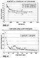
- the reflectivity of the deposited copper films were measured using a 436 nm light source as a function of thickness in angstroms of the copper film.
- the resultant copper film of the invention had a higher reflectivity than the copper films deposited with the prior art blend, as shown in Fig. 2, wherein line A is copper deposited using the blend of the prior art and line B is copper deposited using a blend of the present invention including 1.5% by weight of extra TMVS. It is apparent that the reflectivity, and thus the morphology, of the copper films deposited in accordance with the present invention is improved by about 20%.
- the resistivity of the copper deposited using the same blend of the invention was also compared to blend 2504 as described hereinabove, as shown in Fig. 3.
- the resistivity of copper deposited using 1.5% by weight of extra TMVS expressed in ⁇ -cm versus thickness of the film in angstroms. It is apparent that the copper films deposited in accordance with the invention (line B) have lower resistivity than the copper film deposited using the prior art blend (line A).
- a blend of the present invention and of the prior art were also compared for thermal stability. Copper films were deposited from a blend of 1.5% by weight of extra TMVS and the prior art blend 2504 over TiN barrier layers. The copper coated wafers were heated at 75°C, the same temperature as the vaporizer, for one hour. The copper layer of the present invention had a weight gain of less than 0.1 mg (which is the sensitivity limit of the balance used). The copper layer of the prior art however had a weight gain of 29.2 mg; illustrating the greatly improved thermal stability of the present copper precursors.
- the vaporizer using the present precursor blends more rapidly achieves process pressure for copper deposition than the blend of the prior art.
- the vaporizer could be pumped down more quickly when the present blend is used, as shown in Fig. 4.
- the squares show the pump down time in seconds of the vaporizer using the prior art blend
- the triangles show the pump down time of the vaporizer when the present precursor blend is used, using 1.5% by weight of extra TMVS.
- the data clearly shows that the pump down time of the vaporizer using the present blend stabilizes after about 60 seconds, whereas the vaporizer using the prior art blend does not stabilize until after about 150 seconds.
- down time is reduced and concomitantly throughput is improved, with a reduction in particle formation and residue, leading to improved copper film morphology.
- a blend B was made of hfac-Cu-TMVS and 1.5% of extra TMVS to which a small amount of water was added directly to the processing chamber.
- the resultant copper layer was measured and tested for various parameters which are listed below. A comparison was made to the prior art blend as described above.
- Parameter Blend B Blend 2504 Deposition Rate, ⁇ /min 1000 400 Uniformity, % 5 5 Reflectivity, 1000 ⁇ 115 90 Resistivity, 1500 ⁇ 2.2 ⁇ -cm 2.5 ⁇ -cm Step Coverage, % 100 100 Adhesion as Dep, J/m 2 2.16 2.14 Adhesion after Anneal >5.0 >5.0 Thermal Stability no deposit 29.4mg as dark powder Film Impurity Levels F: 3x10 17 F: 2x10 19 C: 5x10 17 C: 5x10 18 O: 1.3x10 18 O: 5x10 21 Cost per wafer, 500 ⁇ $0.30 $0.69
- the present blend is superior to that of the prior art in several important respects; the deposition rate is 2.5 times higher; the reflectivity is higher; the thermal stability is much higher and the impurities in the copper film are much lower.
- the present blends have improved properties and lower costs, which makes the present method production worthy for state-of-the-art semiconductor devices.
Landscapes
- Chemical & Material Sciences (AREA)
- General Chemical & Material Sciences (AREA)
- Chemical Kinetics & Catalysis (AREA)
- Engineering & Computer Science (AREA)
- Materials Engineering (AREA)
- Mechanical Engineering (AREA)
- Metallurgy (AREA)
- Organic Chemistry (AREA)
- Chemical Vapour Deposition (AREA)
- Electrodes Of Semiconductors (AREA)
Abstract
Description
| Parameter | Blend B | Blend 2504 |
| Deposition Rate, Å/ | 1000 | 400 |
| Uniformity, % | 5 | 5 |
| Reflectivity, 1000Å | 115 | 90 |
| Resistivity, 1500Å | 2.2 µΩ-cm | 2.5µΩ-cm |
| Step Coverage, % | 100 | 100 |
| Adhesion as Dep, J/m2 | 2.16 | 2.14 |
| Adhesion after Anneal | >5.0 | >5.0 |
| Thermal Stability | no deposit | 29.4mg as dark powder |
| Film Impurity Levels | F: 3x10¹⁷ | F: 2x10¹⁹ |
| C: 5x10¹⁷ | C: 5x10¹⁸ | |
| O: 1.3x10¹⁸ | O: 5x10²¹ | |
| Cost per wafer, 500Å | $0.30 | $0.69 |
Thus the present blends have improved properties and lower costs, which makes the present method production worthy for state-of-the-art semiconductor devices.
Claims (6)
- A thermally stable blend of hexafluoroacetylacetonatecopper-trimethylvinylsilane and from about 1.0 to about 5.0 percent by weight of trimethylvinylsilane.
- A blend according to claim 1 containing from about 1.5 to about 2.5 percent by weight of trimethylvinylsilane.
- A method of depositing copper films by chemical vapor deposition comprisingforming a blend of copper hexafluoroacetylacetonate trimethylvinylsilane precursor and a sufficient amount of trimethylvinylsilane to stabilize the precursor,passing said blend to a vaporizer for vaporizing said blend,introducing said blend to a chemical vapor deposition chamber,introducing up to about 2.0 percent by weight of water vapor based on the weight of the precursor blend separately and directly into said chamber, anddepositing a copper film onto a substrate mounted in said chamber.
- A method according to claim 3 wherein from about 1.0 to 5.0 percent by weight of trimethylvinylsilane is added to the copper precursor.
- A method according to claim 4 wherein from about 1.5 to about 2.5 percent by weight of trimethylvinylsilane is added to the copper precursor.
- A method according to claim 3 wherein about 0.5 percent by weight of water vapor based on the amount of precursor blend is introduced to said chamber
Applications Claiming Priority (2)
| Application Number | Priority Date | Filing Date | Title |
|---|---|---|---|
| US09/339,970 US6110530A (en) | 1999-06-25 | 1999-06-25 | CVD method of depositing copper films by using improved organocopper precursor blend |
| US339970 | 2003-01-10 |
Publications (2)
| Publication Number | Publication Date |
|---|---|
| EP1063240A2 true EP1063240A2 (en) | 2000-12-27 |
| EP1063240A3 EP1063240A3 (en) | 2002-11-27 |
Family
ID=23331346
Family Applications (1)
| Application Number | Title | Priority Date | Filing Date |
|---|---|---|---|
| EP00304591A Withdrawn EP1063240A3 (en) | 1999-06-25 | 2000-05-31 | Improved organocopper precursor blend and method of depositing copper by chemical vapor deposition |
Country Status (4)
| Country | Link |
|---|---|
| US (1) | US6110530A (en) |
| EP (1) | EP1063240A3 (en) |
| JP (1) | JP2001026872A (en) |
| KR (1) | KR20010049584A (en) |
Families Citing this family (184)
| Publication number | Priority date | Publication date | Assignee | Title |
|---|---|---|---|---|
| US6291347B1 (en) * | 1999-10-08 | 2001-09-18 | Texas Instruments Incorporated | Method and system for constructing semiconductor devices |
| JP2002105639A (en) * | 2000-09-25 | 2002-04-10 | L'air Liquide | Copper raw material liquid for MOCVD treatment and method for producing the same |
| US6811814B2 (en) | 2001-01-16 | 2004-11-02 | Applied Materials, Inc. | Method for growing thin films by catalytic enhancement |
| US20020127336A1 (en) * | 2001-01-16 | 2002-09-12 | Applied Materials, Inc. | Method for growing thin films by catalytic enhancement |
| KR100424388B1 (en) * | 2001-06-28 | 2004-03-25 | 동부전자 주식회사 | Patterning method by using copper |
| US7138014B2 (en) | 2002-01-28 | 2006-11-21 | Applied Materials, Inc. | Electroless deposition apparatus |
| US6824666B2 (en) * | 2002-01-28 | 2004-11-30 | Applied Materials, Inc. | Electroless deposition method over sub-micron apertures |
| US6899816B2 (en) * | 2002-04-03 | 2005-05-31 | Applied Materials, Inc. | Electroless deposition method |
| US6905622B2 (en) * | 2002-04-03 | 2005-06-14 | Applied Materials, Inc. | Electroless deposition method |
| US6821909B2 (en) * | 2002-10-30 | 2004-11-23 | Applied Materials, Inc. | Post rinse to improve selective deposition of electroless cobalt on copper for ULSI application |
| JP4471975B2 (en) † | 2003-06-30 | 2010-06-02 | ザ プロクター アンド ギャンブル カンパニー | Coated nanofiber web |
| US7827930B2 (en) * | 2004-01-26 | 2010-11-09 | Applied Materials, Inc. | Apparatus for electroless deposition of metals onto semiconductor substrates |
| US7654221B2 (en) * | 2003-10-06 | 2010-02-02 | Applied Materials, Inc. | Apparatus for electroless deposition of metals onto semiconductor substrates |
| US7064065B2 (en) * | 2003-10-15 | 2006-06-20 | Applied Materials, Inc. | Silver under-layers for electroless cobalt alloys |
| US20070111519A1 (en) * | 2003-10-15 | 2007-05-17 | Applied Materials, Inc. | Integrated electroless deposition system |
| US7465358B2 (en) * | 2003-10-15 | 2008-12-16 | Applied Materials, Inc. | Measurement techniques for controlling aspects of a electroless deposition process |
| WO2005038084A2 (en) * | 2003-10-17 | 2005-04-28 | Applied Materials, Inc. | Selective self-initiating electroless capping of copper with cobalt-containing alloys |
| US7205233B2 (en) | 2003-11-07 | 2007-04-17 | Applied Materials, Inc. | Method for forming CoWRe alloys by electroless deposition |
| US20060003570A1 (en) * | 2003-12-02 | 2006-01-05 | Arulkumar Shanmugasundram | Method and apparatus for electroless capping with vapor drying |
| US20050161338A1 (en) * | 2004-01-26 | 2005-07-28 | Applied Materials, Inc. | Electroless cobalt alloy deposition process |
| US20050230350A1 (en) | 2004-02-26 | 2005-10-20 | Applied Materials, Inc. | In-situ dry clean chamber for front end of line fabrication |
| US7166732B2 (en) * | 2004-06-16 | 2007-01-23 | Advanced Technology Materials, Inc. | Copper (I) compounds useful as deposition precursors of copper thin films |
| US20060162658A1 (en) * | 2005-01-27 | 2006-07-27 | Applied Materials, Inc. | Ruthenium layer deposition apparatus and method |
| US7438949B2 (en) * | 2005-01-27 | 2008-10-21 | Applied Materials, Inc. | Ruthenium containing layer deposition method |
| US7651934B2 (en) | 2005-03-18 | 2010-01-26 | Applied Materials, Inc. | Process for electroless copper deposition |
| US20060252252A1 (en) | 2005-03-18 | 2006-11-09 | Zhize Zhu | Electroless deposition processes and compositions for forming interconnects |
| WO2006102318A2 (en) | 2005-03-18 | 2006-09-28 | Applied Materials, Inc. | Electroless deposition process on a contact containing silicon or silicide |
| WO2007035880A2 (en) * | 2005-09-21 | 2007-03-29 | Applied Materials, Inc. | Method and apparatus for forming device features in an integrated electroless deposition system |
| TW200745140A (en) * | 2006-06-02 | 2007-12-16 | Advanced Tech Materials | Copper (I) amidinates and guanidinates, mixed ligand copper complexes, and compositions for chemical vapor deposition, atomic layer deposition, and rapid vapor deposition of copper |
| JP5151082B2 (en) * | 2006-07-20 | 2013-02-27 | 東京エレクトロン株式会社 | Film forming method, film forming apparatus, and storage medium |
| WO2008069821A1 (en) * | 2006-12-05 | 2008-06-12 | Advanced Technology Materials, Inc. | Metal aminotroponiminates, bis-oxazolinates and guanidinates |
| US7867900B2 (en) * | 2007-09-28 | 2011-01-11 | Applied Materials, Inc. | Aluminum contact integration on cobalt silicide junction |
| US9324576B2 (en) | 2010-05-27 | 2016-04-26 | Applied Materials, Inc. | Selective etch for silicon films |
| US10283321B2 (en) | 2011-01-18 | 2019-05-07 | Applied Materials, Inc. | Semiconductor processing system and methods using capacitively coupled plasma |
| US8771539B2 (en) | 2011-02-22 | 2014-07-08 | Applied Materials, Inc. | Remotely-excited fluorine and water vapor etch |
| US8999856B2 (en) | 2011-03-14 | 2015-04-07 | Applied Materials, Inc. | Methods for etch of sin films |
| US9064815B2 (en) | 2011-03-14 | 2015-06-23 | Applied Materials, Inc. | Methods for etch of metal and metal-oxide films |
| US8771536B2 (en) | 2011-08-01 | 2014-07-08 | Applied Materials, Inc. | Dry-etch for silicon-and-carbon-containing films |
| US8679982B2 (en) | 2011-08-26 | 2014-03-25 | Applied Materials, Inc. | Selective suppression of dry-etch rate of materials containing both silicon and oxygen |
| US8679983B2 (en) | 2011-09-01 | 2014-03-25 | Applied Materials, Inc. | Selective suppression of dry-etch rate of materials containing both silicon and nitrogen |
| US8927390B2 (en) | 2011-09-26 | 2015-01-06 | Applied Materials, Inc. | Intrench profile |
| US8808563B2 (en) | 2011-10-07 | 2014-08-19 | Applied Materials, Inc. | Selective etch of silicon by way of metastable hydrogen termination |
| WO2013070436A1 (en) | 2011-11-08 | 2013-05-16 | Applied Materials, Inc. | Methods of reducing substrate dislocation during gapfill processing |
| US9267739B2 (en) | 2012-07-18 | 2016-02-23 | Applied Materials, Inc. | Pedestal with multi-zone temperature control and multiple purge capabilities |
| US9373517B2 (en) | 2012-08-02 | 2016-06-21 | Applied Materials, Inc. | Semiconductor processing with DC assisted RF power for improved control |
| US9034770B2 (en) | 2012-09-17 | 2015-05-19 | Applied Materials, Inc. | Differential silicon oxide etch |
| US9023734B2 (en) | 2012-09-18 | 2015-05-05 | Applied Materials, Inc. | Radical-component oxide etch |
| US9390937B2 (en) | 2012-09-20 | 2016-07-12 | Applied Materials, Inc. | Silicon-carbon-nitride selective etch |
| US9132436B2 (en) | 2012-09-21 | 2015-09-15 | Applied Materials, Inc. | Chemical control features in wafer process equipment |
| US8765574B2 (en) | 2012-11-09 | 2014-07-01 | Applied Materials, Inc. | Dry etch process |
| US8969212B2 (en) | 2012-11-20 | 2015-03-03 | Applied Materials, Inc. | Dry-etch selectivity |
| US9064816B2 (en) | 2012-11-30 | 2015-06-23 | Applied Materials, Inc. | Dry-etch for selective oxidation removal |
| US8980763B2 (en) | 2012-11-30 | 2015-03-17 | Applied Materials, Inc. | Dry-etch for selective tungsten removal |
| US9111877B2 (en) | 2012-12-18 | 2015-08-18 | Applied Materials, Inc. | Non-local plasma oxide etch |
| US8921234B2 (en) | 2012-12-21 | 2014-12-30 | Applied Materials, Inc. | Selective titanium nitride etching |
| US10256079B2 (en) | 2013-02-08 | 2019-04-09 | Applied Materials, Inc. | Semiconductor processing systems having multiple plasma configurations |
| US9362130B2 (en) | 2013-03-01 | 2016-06-07 | Applied Materials, Inc. | Enhanced etching processes using remote plasma sources |
| US9040422B2 (en) | 2013-03-05 | 2015-05-26 | Applied Materials, Inc. | Selective titanium nitride removal |
| US8801952B1 (en) | 2013-03-07 | 2014-08-12 | Applied Materials, Inc. | Conformal oxide dry etch |
| US10170282B2 (en) | 2013-03-08 | 2019-01-01 | Applied Materials, Inc. | Insulated semiconductor faceplate designs |
| US20140271097A1 (en) | 2013-03-15 | 2014-09-18 | Applied Materials, Inc. | Processing systems and methods for halide scavenging |
| US8895449B1 (en) | 2013-05-16 | 2014-11-25 | Applied Materials, Inc. | Delicate dry clean |
| US9114438B2 (en) | 2013-05-21 | 2015-08-25 | Applied Materials, Inc. | Copper residue chamber clean |
| US9493879B2 (en) | 2013-07-12 | 2016-11-15 | Applied Materials, Inc. | Selective sputtering for pattern transfer |
| US9773648B2 (en) | 2013-08-30 | 2017-09-26 | Applied Materials, Inc. | Dual discharge modes operation for remote plasma |
| US8956980B1 (en) | 2013-09-16 | 2015-02-17 | Applied Materials, Inc. | Selective etch of silicon nitride |
| US8951429B1 (en) | 2013-10-29 | 2015-02-10 | Applied Materials, Inc. | Tungsten oxide processing |
| US9236265B2 (en) | 2013-11-04 | 2016-01-12 | Applied Materials, Inc. | Silicon germanium processing |
| US9576809B2 (en) | 2013-11-04 | 2017-02-21 | Applied Materials, Inc. | Etch suppression with germanium |
| US9520303B2 (en) | 2013-11-12 | 2016-12-13 | Applied Materials, Inc. | Aluminum selective etch |
| US9245762B2 (en) | 2013-12-02 | 2016-01-26 | Applied Materials, Inc. | Procedure for etch rate consistency |
| US9117855B2 (en) | 2013-12-04 | 2015-08-25 | Applied Materials, Inc. | Polarity control for remote plasma |
| US9287095B2 (en) | 2013-12-17 | 2016-03-15 | Applied Materials, Inc. | Semiconductor system assemblies and methods of operation |
| US9263278B2 (en) | 2013-12-17 | 2016-02-16 | Applied Materials, Inc. | Dopant etch selectivity control |
| US9190293B2 (en) | 2013-12-18 | 2015-11-17 | Applied Materials, Inc. | Even tungsten etch for high aspect ratio trenches |
| US9287134B2 (en) | 2014-01-17 | 2016-03-15 | Applied Materials, Inc. | Titanium oxide etch |
| US9396989B2 (en) | 2014-01-27 | 2016-07-19 | Applied Materials, Inc. | Air gaps between copper lines |
| US9293568B2 (en) | 2014-01-27 | 2016-03-22 | Applied Materials, Inc. | Method of fin patterning |
| US9385028B2 (en) | 2014-02-03 | 2016-07-05 | Applied Materials, Inc. | Air gap process |
| US9499898B2 (en) | 2014-03-03 | 2016-11-22 | Applied Materials, Inc. | Layered thin film heater and method of fabrication |
| US9299575B2 (en) | 2014-03-17 | 2016-03-29 | Applied Materials, Inc. | Gas-phase tungsten etch |
| US9299538B2 (en) | 2014-03-20 | 2016-03-29 | Applied Materials, Inc. | Radial waveguide systems and methods for post-match control of microwaves |
| US9299537B2 (en) | 2014-03-20 | 2016-03-29 | Applied Materials, Inc. | Radial waveguide systems and methods for post-match control of microwaves |
| US9136273B1 (en) | 2014-03-21 | 2015-09-15 | Applied Materials, Inc. | Flash gate air gap |
| US9903020B2 (en) | 2014-03-31 | 2018-02-27 | Applied Materials, Inc. | Generation of compact alumina passivation layers on aluminum plasma equipment components |
| US9269590B2 (en) | 2014-04-07 | 2016-02-23 | Applied Materials, Inc. | Spacer formation |
| US9309598B2 (en) | 2014-05-28 | 2016-04-12 | Applied Materials, Inc. | Oxide and metal removal |
| US9847289B2 (en) | 2014-05-30 | 2017-12-19 | Applied Materials, Inc. | Protective via cap for improved interconnect performance |
| US9406523B2 (en) | 2014-06-19 | 2016-08-02 | Applied Materials, Inc. | Highly selective doped oxide removal method |
| US9378969B2 (en) | 2014-06-19 | 2016-06-28 | Applied Materials, Inc. | Low temperature gas-phase carbon removal |
| US9425058B2 (en) | 2014-07-24 | 2016-08-23 | Applied Materials, Inc. | Simplified litho-etch-litho-etch process |
| US9159606B1 (en) | 2014-07-31 | 2015-10-13 | Applied Materials, Inc. | Metal air gap |
| US9378978B2 (en) | 2014-07-31 | 2016-06-28 | Applied Materials, Inc. | Integrated oxide recess and floating gate fin trimming |
| US9496167B2 (en) | 2014-07-31 | 2016-11-15 | Applied Materials, Inc. | Integrated bit-line airgap formation and gate stack post clean |
| US9165786B1 (en) | 2014-08-05 | 2015-10-20 | Applied Materials, Inc. | Integrated oxide and nitride recess for better channel contact in 3D architectures |
| US9659753B2 (en) | 2014-08-07 | 2017-05-23 | Applied Materials, Inc. | Grooved insulator to reduce leakage current |
| US9553102B2 (en) | 2014-08-19 | 2017-01-24 | Applied Materials, Inc. | Tungsten separation |
| US9355856B2 (en) | 2014-09-12 | 2016-05-31 | Applied Materials, Inc. | V trench dry etch |
| US9368364B2 (en) | 2014-09-24 | 2016-06-14 | Applied Materials, Inc. | Silicon etch process with tunable selectivity to SiO2 and other materials |
| US9478434B2 (en) | 2014-09-24 | 2016-10-25 | Applied Materials, Inc. | Chlorine-based hardmask removal |
| US9613822B2 (en) | 2014-09-25 | 2017-04-04 | Applied Materials, Inc. | Oxide etch selectivity enhancement |
| US9966240B2 (en) | 2014-10-14 | 2018-05-08 | Applied Materials, Inc. | Systems and methods for internal surface conditioning assessment in plasma processing equipment |
| US9355922B2 (en) | 2014-10-14 | 2016-05-31 | Applied Materials, Inc. | Systems and methods for internal surface conditioning in plasma processing equipment |
| US10103057B2 (en) | 2014-11-11 | 2018-10-16 | The Board Of Trustees Of The University Of Illinois | Use of an inhibitor molecule in chemical vapor deposition to afford deposition of copper on a metal substrate with no deposition on adjacent SIO2 substrate |
| US11637002B2 (en) | 2014-11-26 | 2023-04-25 | Applied Materials, Inc. | Methods and systems to enhance process uniformity |
| US9299583B1 (en) | 2014-12-05 | 2016-03-29 | Applied Materials, Inc. | Aluminum oxide selective etch |
| US10573496B2 (en) | 2014-12-09 | 2020-02-25 | Applied Materials, Inc. | Direct outlet toroidal plasma source |
| US10224210B2 (en) | 2014-12-09 | 2019-03-05 | Applied Materials, Inc. | Plasma processing system with direct outlet toroidal plasma source |
| US9502258B2 (en) | 2014-12-23 | 2016-11-22 | Applied Materials, Inc. | Anisotropic gap etch |
| US9343272B1 (en) | 2015-01-08 | 2016-05-17 | Applied Materials, Inc. | Self-aligned process |
| US11257693B2 (en) | 2015-01-09 | 2022-02-22 | Applied Materials, Inc. | Methods and systems to improve pedestal temperature control |
| US9373522B1 (en) | 2015-01-22 | 2016-06-21 | Applied Mateials, Inc. | Titanium nitride removal |
| US9449846B2 (en) | 2015-01-28 | 2016-09-20 | Applied Materials, Inc. | Vertical gate separation |
| US9728437B2 (en) | 2015-02-03 | 2017-08-08 | Applied Materials, Inc. | High temperature chuck for plasma processing systems |
| US20160225652A1 (en) | 2015-02-03 | 2016-08-04 | Applied Materials, Inc. | Low temperature chuck for plasma processing systems |
| US9881805B2 (en) | 2015-03-02 | 2018-01-30 | Applied Materials, Inc. | Silicon selective removal |
| US9741593B2 (en) | 2015-08-06 | 2017-08-22 | Applied Materials, Inc. | Thermal management systems and methods for wafer processing systems |
| US9691645B2 (en) | 2015-08-06 | 2017-06-27 | Applied Materials, Inc. | Bolted wafer chuck thermal management systems and methods for wafer processing systems |
| US9349605B1 (en) | 2015-08-07 | 2016-05-24 | Applied Materials, Inc. | Oxide etch selectivity systems and methods |
| US10504700B2 (en) | 2015-08-27 | 2019-12-10 | Applied Materials, Inc. | Plasma etching systems and methods with secondary plasma injection |
| US10522371B2 (en) | 2016-05-19 | 2019-12-31 | Applied Materials, Inc. | Systems and methods for improved semiconductor etching and component protection |
| US10504754B2 (en) | 2016-05-19 | 2019-12-10 | Applied Materials, Inc. | Systems and methods for improved semiconductor etching and component protection |
| US9865484B1 (en) | 2016-06-29 | 2018-01-09 | Applied Materials, Inc. | Selective etch using material modification and RF pulsing |
| US10062575B2 (en) | 2016-09-09 | 2018-08-28 | Applied Materials, Inc. | Poly directional etch by oxidation |
| US10629473B2 (en) | 2016-09-09 | 2020-04-21 | Applied Materials, Inc. | Footing removal for nitride spacer |
| US10546729B2 (en) | 2016-10-04 | 2020-01-28 | Applied Materials, Inc. | Dual-channel showerhead with improved profile |
| US10062585B2 (en) | 2016-10-04 | 2018-08-28 | Applied Materials, Inc. | Oxygen compatible plasma source |
| US9721789B1 (en) | 2016-10-04 | 2017-08-01 | Applied Materials, Inc. | Saving ion-damaged spacers |
| US9934942B1 (en) | 2016-10-04 | 2018-04-03 | Applied Materials, Inc. | Chamber with flow-through source |
| US10062579B2 (en) | 2016-10-07 | 2018-08-28 | Applied Materials, Inc. | Selective SiN lateral recess |
| US9947549B1 (en) | 2016-10-10 | 2018-04-17 | Applied Materials, Inc. | Cobalt-containing material removal |
| US9768034B1 (en) | 2016-11-11 | 2017-09-19 | Applied Materials, Inc. | Removal methods for high aspect ratio structures |
| US10163696B2 (en) | 2016-11-11 | 2018-12-25 | Applied Materials, Inc. | Selective cobalt removal for bottom up gapfill |
| US10242908B2 (en) | 2016-11-14 | 2019-03-26 | Applied Materials, Inc. | Airgap formation with damage-free copper |
| US10026621B2 (en) | 2016-11-14 | 2018-07-17 | Applied Materials, Inc. | SiN spacer profile patterning |
| US10566206B2 (en) | 2016-12-27 | 2020-02-18 | Applied Materials, Inc. | Systems and methods for anisotropic material breakthrough |
| US10403507B2 (en) | 2017-02-03 | 2019-09-03 | Applied Materials, Inc. | Shaped etch profile with oxidation |
| US10431429B2 (en) | 2017-02-03 | 2019-10-01 | Applied Materials, Inc. | Systems and methods for radial and azimuthal control of plasma uniformity |
| US10043684B1 (en) | 2017-02-06 | 2018-08-07 | Applied Materials, Inc. | Self-limiting atomic thermal etching systems and methods |
| US10319739B2 (en) | 2017-02-08 | 2019-06-11 | Applied Materials, Inc. | Accommodating imperfectly aligned memory holes |
| US10943834B2 (en) | 2017-03-13 | 2021-03-09 | Applied Materials, Inc. | Replacement contact process |
| US10319649B2 (en) | 2017-04-11 | 2019-06-11 | Applied Materials, Inc. | Optical emission spectroscopy (OES) for remote plasma monitoring |
| US11276559B2 (en) | 2017-05-17 | 2022-03-15 | Applied Materials, Inc. | Semiconductor processing chamber for multiple precursor flow |
| US11276590B2 (en) | 2017-05-17 | 2022-03-15 | Applied Materials, Inc. | Multi-zone semiconductor substrate supports |
| JP7176860B6 (en) | 2017-05-17 | 2022-12-16 | アプライド マテリアルズ インコーポレイテッド | Semiconductor processing chamber to improve precursor flow |
| US10497579B2 (en) | 2017-05-31 | 2019-12-03 | Applied Materials, Inc. | Water-free etching methods |
| US10049891B1 (en) | 2017-05-31 | 2018-08-14 | Applied Materials, Inc. | Selective in situ cobalt residue removal |
| US10920320B2 (en) | 2017-06-16 | 2021-02-16 | Applied Materials, Inc. | Plasma health determination in semiconductor substrate processing reactors |
| US10541246B2 (en) | 2017-06-26 | 2020-01-21 | Applied Materials, Inc. | 3D flash memory cells which discourage cross-cell electrical tunneling |
| US10727080B2 (en) | 2017-07-07 | 2020-07-28 | Applied Materials, Inc. | Tantalum-containing material removal |
| US10541184B2 (en) | 2017-07-11 | 2020-01-21 | Applied Materials, Inc. | Optical emission spectroscopic techniques for monitoring etching |
| US10354889B2 (en) | 2017-07-17 | 2019-07-16 | Applied Materials, Inc. | Non-halogen etching of silicon-containing materials |
| US10043674B1 (en) | 2017-08-04 | 2018-08-07 | Applied Materials, Inc. | Germanium etching systems and methods |
| US10170336B1 (en) | 2017-08-04 | 2019-01-01 | Applied Materials, Inc. | Methods for anisotropic control of selective silicon removal |
| US10297458B2 (en) | 2017-08-07 | 2019-05-21 | Applied Materials, Inc. | Process window widening using coated parts in plasma etch processes |
| US10128086B1 (en) | 2017-10-24 | 2018-11-13 | Applied Materials, Inc. | Silicon pretreatment for nitride removal |
| US10283324B1 (en) | 2017-10-24 | 2019-05-07 | Applied Materials, Inc. | Oxygen treatment for nitride etching |
| US11584986B1 (en) | 2017-11-01 | 2023-02-21 | The Board Of Trustees Of The University Of Illinois | Area selective CVD of metallic films using precursor gases and inhibitors |
| US10256112B1 (en) | 2017-12-08 | 2019-04-09 | Applied Materials, Inc. | Selective tungsten removal |
| US10903054B2 (en) | 2017-12-19 | 2021-01-26 | Applied Materials, Inc. | Multi-zone gas distribution systems and methods |
| US11328909B2 (en) | 2017-12-22 | 2022-05-10 | Applied Materials, Inc. | Chamber conditioning and removal processes |
| US10854426B2 (en) | 2018-01-08 | 2020-12-01 | Applied Materials, Inc. | Metal recess for semiconductor structures |
| US10964512B2 (en) | 2018-02-15 | 2021-03-30 | Applied Materials, Inc. | Semiconductor processing chamber multistage mixing apparatus and methods |
| US10679870B2 (en) | 2018-02-15 | 2020-06-09 | Applied Materials, Inc. | Semiconductor processing chamber multistage mixing apparatus |
| TWI716818B (en) | 2018-02-28 | 2021-01-21 | 美商應用材料股份有限公司 | Systems and methods to form airgaps |
| US10593560B2 (en) | 2018-03-01 | 2020-03-17 | Applied Materials, Inc. | Magnetic induction plasma source for semiconductor processes and equipment |
| US10319600B1 (en) | 2018-03-12 | 2019-06-11 | Applied Materials, Inc. | Thermal silicon etch |
| US10497573B2 (en) | 2018-03-13 | 2019-12-03 | Applied Materials, Inc. | Selective atomic layer etching of semiconductor materials |
| US10573527B2 (en) | 2018-04-06 | 2020-02-25 | Applied Materials, Inc. | Gas-phase selective etching systems and methods |
| US10490406B2 (en) | 2018-04-10 | 2019-11-26 | Appled Materials, Inc. | Systems and methods for material breakthrough |
| US10699879B2 (en) | 2018-04-17 | 2020-06-30 | Applied Materials, Inc. | Two piece electrode assembly with gap for plasma control |
| US10886137B2 (en) | 2018-04-30 | 2021-01-05 | Applied Materials, Inc. | Selective nitride removal |
| US10872778B2 (en) | 2018-07-06 | 2020-12-22 | Applied Materials, Inc. | Systems and methods utilizing solid-phase etchants |
| US10755941B2 (en) | 2018-07-06 | 2020-08-25 | Applied Materials, Inc. | Self-limiting selective etching systems and methods |
| US10672642B2 (en) | 2018-07-24 | 2020-06-02 | Applied Materials, Inc. | Systems and methods for pedestal configuration |
| US10892198B2 (en) | 2018-09-14 | 2021-01-12 | Applied Materials, Inc. | Systems and methods for improved performance in semiconductor processing |
| US11049755B2 (en) | 2018-09-14 | 2021-06-29 | Applied Materials, Inc. | Semiconductor substrate supports with embedded RF shield |
| US11062887B2 (en) | 2018-09-17 | 2021-07-13 | Applied Materials, Inc. | High temperature RF heater pedestals |
| US11417534B2 (en) | 2018-09-21 | 2022-08-16 | Applied Materials, Inc. | Selective material removal |
| US11682560B2 (en) | 2018-10-11 | 2023-06-20 | Applied Materials, Inc. | Systems and methods for hafnium-containing film removal |
| US11121002B2 (en) | 2018-10-24 | 2021-09-14 | Applied Materials, Inc. | Systems and methods for etching metals and metal derivatives |
| US11437242B2 (en) | 2018-11-27 | 2022-09-06 | Applied Materials, Inc. | Selective removal of silicon-containing materials |
| US11721527B2 (en) | 2019-01-07 | 2023-08-08 | Applied Materials, Inc. | Processing chamber mixing systems |
| US10920319B2 (en) | 2019-01-11 | 2021-02-16 | Applied Materials, Inc. | Ceramic showerheads with conductive electrodes |
Family Cites Families (6)
| Publication number | Priority date | Publication date | Assignee | Title |
|---|---|---|---|---|
| US35614A (en) * | 1862-06-17 | Improvement in surgical splints | ||
| US5098516A (en) * | 1990-12-31 | 1992-03-24 | Air Products And Chemicals, Inc. | Processes for the chemical vapor deposition of copper and etching of copper |
| US5085731A (en) * | 1991-02-04 | 1992-02-04 | Air Products And Chemicals, Inc. | Volatile liquid precursors for the chemical vapor deposition of copper |
| US5322712A (en) | 1993-05-18 | 1994-06-21 | Air Products And Chemicals, Inc. | Process for improved quality of CVD copper films |
| JPH09296269A (en) * | 1996-04-30 | 1997-11-18 | Toshiba Corp | Method for forming copper thin film |
| US5744192A (en) * | 1996-11-08 | 1998-04-28 | Sharp Microelectronics Technology, Inc. | Method of using water vapor to increase the conductivity of cooper desposited with cu(hfac)TMVS |
-
1999
- 1999-06-25 US US09/339,970 patent/US6110530A/en not_active Expired - Fee Related
-
2000
- 2000-05-31 EP EP00304591A patent/EP1063240A3/en not_active Withdrawn
- 2000-06-15 JP JP2000179505A patent/JP2001026872A/en not_active Withdrawn
- 2000-06-21 KR KR1020000034116A patent/KR20010049584A/en not_active Withdrawn
Also Published As
| Publication number | Publication date |
|---|---|
| EP1063240A3 (en) | 2002-11-27 |
| KR20010049584A (en) | 2001-06-15 |
| JP2001026872A (en) | 2001-01-30 |
| US6110530A (en) | 2000-08-29 |
Similar Documents
| Publication | Publication Date | Title |
|---|---|---|
| US6110530A (en) | CVD method of depositing copper films by using improved organocopper precursor blend | |
| US6534133B1 (en) | Methodology for in-situ doping of aluminum coatings | |
| CN1174117C (en) | Plasma treatment of thermal chemical vapor deposited tantalum nitride films from tantalum halide precursors | |
| US7279421B2 (en) | Method and deposition system for increasing deposition rates of metal layers from metal-carbonyl precursors | |
| EP1185722B1 (en) | Pecvd of tan films from tantalum halide precursors | |
| JPH0748672A (en) | Chemical vapor deposition of copper film | |
| JP2002536549A (en) | Chemical vapor deposition of tungsten nitride | |
| US7763311B2 (en) | Method for heating a substrate prior to a vapor deposition process | |
| EP0566040A2 (en) | Process for selectively depositing copper aluminum alloy onto a substrate | |
| US8283485B2 (en) | Process for selectively depositing copper thin films on substrates with copper and ruthenium areas via vapor deposition | |
| KR100256669B1 (en) | Chemical vapor deposition apparatus and method for forming copper film using the same | |
| JP3844292B2 (en) | Method for depositing high adhesion copper thin film on metal nitride substrate and copper metal precursor mixture | |
| Awaya et al. | The effect of adding hexafluoroacetylacetone on chemical vapor deposition of copper using Cu (I) and Cu (II) precursor systems | |
| US20070237895A1 (en) | Method and system for initiating a deposition process utilizing a metal carbonyl precursor | |
| US6576293B2 (en) | Method to improve copper thin film adhesion to metal nitride substrates by the addition of water | |
| US20080241380A1 (en) | Method for performing a vapor deposition process | |
| US6071562A (en) | Process for depositing titanium nitride films | |
| Naik et al. | Texture and surface morphology improvement of Al by two-stage chemical vapor deposition and its integration in an Al plug-interconnect scheme for sub 0.25 μm metallization | |
| EP1047807B1 (en) | A DEPOSITION METHOD FOR USING A Cu(hfac) PRECURSOR WITH A SUBSTITUTED PHENYLETHYLENE LIGAND | |
| JPS63109172A (en) | Low pressure chemical vapor deposition of metal silicide | |
| TW574409B (en) | Method for incorporating silicon into CVD metal films | |
| US6720031B2 (en) | Method of controlling the initial growth of CVD copper films by surface treatment of barrier metals films | |
| Zhang et al. | Optimization of copper CVD film properties using the precursor of Cu (hfac)(tmvs) with variations of additive content | |
| US6171958B1 (en) | Process for preparation of diffusion barrier for semiconductor | |
| JP2677230B2 (en) | Method for forming TiN film |
Legal Events
| Date | Code | Title | Description |
|---|---|---|---|
| PUAI | Public reference made under article 153(3) epc to a published international application that has entered the european phase |
Free format text: ORIGINAL CODE: 0009012 |
|
| AK | Designated contracting states |
Kind code of ref document: A2 Designated state(s): AT BE CH CY DE DK ES FI FR GB GR IE IT LI LU MC NL PT SE |
|
| AX | Request for extension of the european patent |
Free format text: AL;LT;LV;MK;RO;SI |
|
| PUAL | Search report despatched |
Free format text: ORIGINAL CODE: 0009013 |
|
| RIC1 | Information provided on ipc code assigned before grant |
Free format text: 7C 07F 7/08 A, 7C 23C 16/44 B, 7C 23C 16/448 B |
|
| AK | Designated contracting states |
Kind code of ref document: A3 Designated state(s): AT BE CH CY DE DK ES FI FR GB GR IE IT LI LU MC NL PT SE |
|
| AX | Request for extension of the european patent |
Free format text: AL;LT;LV;MK;RO;SI |
|
| STAA | Information on the status of an ep patent application or granted ep patent |
Free format text: STATUS: THE APPLICATION HAS BEEN WITHDRAWN |
|
| 17P | Request for examination filed |
Effective date: 20030527 |
|
| 18W | Application withdrawn |
Effective date: 20030611 |