EP1061695A2 - Method and apparatus for maintaining packet order integrity in a parallel switching engine - Google Patents
Method and apparatus for maintaining packet order integrity in a parallel switching engine Download PDFInfo
- Publication number
- EP1061695A2 EP1061695A2 EP00110566A EP00110566A EP1061695A2 EP 1061695 A2 EP1061695 A2 EP 1061695A2 EP 00110566 A EP00110566 A EP 00110566A EP 00110566 A EP00110566 A EP 00110566A EP 1061695 A2 EP1061695 A2 EP 1061695A2
- Authority
- EP
- European Patent Office
- Prior art keywords
- packet
- processing element
- source
- inbound
- packets
- Prior art date
- Legal status (The legal status is an assumption and is not a legal conclusion. Google has not performed a legal analysis and makes no representation as to the accuracy of the status listed.)
- Granted
Links
Images


Classifications
-
- H—ELECTRICITY
- H04—ELECTRIC COMMUNICATION TECHNIQUE
- H04L—TRANSMISSION OF DIGITAL INFORMATION, e.g. TELEGRAPHIC COMMUNICATION
- H04L49/00—Packet switching elements
- H04L49/15—Interconnection of switching modules
- H04L49/1515—Non-blocking multistage, e.g. Clos
- H04L49/153—ATM switching fabrics having parallel switch planes
-
- H—ELECTRICITY
- H04—ELECTRIC COMMUNICATION TECHNIQUE
- H04L—TRANSMISSION OF DIGITAL INFORMATION, e.g. TELEGRAPHIC COMMUNICATION
- H04L49/00—Packet switching elements
- H04L49/30—Peripheral units, e.g. input or output ports
-
- H—ELECTRICITY
- H04—ELECTRIC COMMUNICATION TECHNIQUE
- H04L—TRANSMISSION OF DIGITAL INFORMATION, e.g. TELEGRAPHIC COMMUNICATION
- H04L12/00—Data switching networks
- H04L12/54—Store-and-forward switching systems
- H04L12/56—Packet switching systems
- H04L12/5601—Transfer mode dependent, e.g. ATM
- H04L2012/5638—Services, e.g. multimedia, GOS, QOS
- H04L2012/5646—Cell characteristics, e.g. loss, delay, jitter, sequence integrity
- H04L2012/565—Sequence integrity
-
- H—ELECTRICITY
- H04—ELECTRIC COMMUNICATION TECHNIQUE
- H04L—TRANSMISSION OF DIGITAL INFORMATION, e.g. TELEGRAPHIC COMMUNICATION
- H04L49/00—Packet switching elements
- H04L49/10—Packet switching elements characterised by the switching fabric construction
- H04L49/102—Packet switching elements characterised by the switching fabric construction using shared medium, e.g. bus or ring
-
- H—ELECTRICITY
- H04—ELECTRIC COMMUNICATION TECHNIQUE
- H04L—TRANSMISSION OF DIGITAL INFORMATION, e.g. TELEGRAPHIC COMMUNICATION
- H04L49/00—Packet switching elements
- H04L49/30—Peripheral units, e.g. input or output ports
- H04L49/3009—Header conversion, routing tables or routing tags
Definitions
- the present invention relates to data switching, and more particularly to data switching engines of the kind in which a processor array is used to switch data from a plurality of sources to a plurality of destinations in a data communication network.
- Processor array switching engines provide certain advantages over ASIC switching engines in terms of time-to-market, flexibility and scalability. Still, the "parallel" aspect of processor array switching engines creates technical challenges. Foremost among these is how to best allocate the resources of the array.
- One possibility is to strictly dedicate each processor in the array to a particular group of sources. However, such a dedicated processor array is inefficient since a processor is idle whenever the sources to which it is dedicated are not transmitting packets, even while other processors may be overburdened.
- a second possibility is to allow each processor in the array to be shared by all sources. Such a shared processor array might greatly increase overall switching efficiency, especially when implemented in conjunction with an efficient load balancing algorithm ensuring that inbound packets are transmitted to the processors presently being underutilized.
- a shared processor array gives rise to other problems, such as how to preserve packet order integrity.
- a problem of preserving packet order integrity arises in shared processor arrays because at any given time in the operational cycle of such an array, the time required to process a packet will vary from processor-to-processor. Thus, packets may be switched out of the array in an order different from that in which they were transmitted to the array for switching. While a departure from strict "first in, first out" sequencing is not a problem for packets applicable to different conversations, it may be for packets applicable to the same conversation.
- the present invention provides a method and apparatus for preserving packet order integrity in a shared processor array.
- the order for packets relating to the same conversation is maintained by checking for each inbound packet whether a previous packet from the same source is pending at a processing element before forwarding the packet to the processor array. If the check reveals that such a packet is pending, the inbound packet is forwarded to the same processing element as the previous packet. If the check reveals that no packet from the same source is pending at any processing element, the inbound packet is forwarded to a processing element in accordance with a load balancing algorithm.
- an input unit 110 and output unit 120 for a data switching architecture are shown.
- one or more input units and one or more output units are coupled via a switch fabric 130 such that every physical input (and its associated input unit) may transfer data to every physical output (and its associated output unit).
- a subset (or all) of input units receive data destined for a subset (or all) output units. Data may therefore be imagined as flowing from left to right, for example, from input unit 110 to output unit 120.
- Each input unit has a plurality of physical inputs and each output unit has one or more physical outputs.
- Data may be transmitted through the architecture in variable length packets, in fixed length cells, or both, although any such discrete unit of data will be referred to as a "packet" herein for clarity and consistency.
- packet a packet received on one of the physical inputs and destined for the physical output arrives at processor array module 112 and is switched and forwarded to input buffer 114.
- the packet is eventually released on fabric data bus 142 to switching fabric 130 and arrives at output buffer 122, where the packet remains stored until eventual delivery on the physical output.
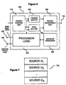
- processor array module 112 is shown in greater detail.
- Processor array module 112 is responsible for switching packets from physical inputs to physical outputs. In its most basic feature, the switching operation performed in module 112 involves interpreting and modifying packet control fields, such addresses encoded in packet headers, to ensure delivery of packets on appropriate physical outputs.
- Processor array module 112 has M input controllers 210 associated with physical inputs. Input control units 210 are coupled via L module data buses 220 to processor array 230 which includes L processing elements. Module data buses 220 are arranged such that each processing element receives data on a particular bus and each input controller may transmit data on each bus. Processing elements 230 share external data bus 142 for forwarding packets to input buffer 114 after the packet switching operation has been completed.
- An important object of the invention is to implement a shared processor array which preserves the sequence of packets applicable to the same conversation. This preservation of packet order integrity is achieved in a preferred embodiment by implementing a "commit-and-release" protocol.
- Input controllers 210 deliver packets from different sources to processor array 230. Uncommitted sources become committed to a particular processing element in array 230 upon forwarding an inbound packet from the source to the element. All subsequent inbound packets from the source are forwarded to the element while the commitment is in effect. The commitment is terminated after all packets from the source have been switched out of the array.
- This "commit-and-release" protocol guarantees that packets applicable to the same conversation are switched out of a shared array processor array in their order of arrival without unduly hindering switching performance.
- input controllers 210 and processing elements in array 230 are coupled by control lines.
- a representative input controller 310 and processing element 320 are coupled by mask reset line 322 and backlog update line 324.
- Processing element 320 invokes lines 322, 324 to provide feedback to input controller 310 about current conditions at element 320 which controller 310 must know to correctly decide which processing element within array 230 to select when forwarding inbound packets.
- mask reset line 322 is invoked to instruct controller 310 that element 320 has no more packets pending from the source.
- Backlog update line 324 is invoked to inform controller 310 about the current backlog of packets pending in element 320 from sources associated with all input controllers 210.
- controller 310 compares backlog information provided by all processing elements in array 230 to assess the relative efficiency of forwarding inbound packets from the source to element 320.
- processor array module 210 The operation of processor array module 210 will now be described in even more detail by reference to Figures 4-10.
- a representative input controller 400 is illustrated. Inbound packets arrive at controller 400 on physical input IP_IN and are written to input queue 404 and write address counter 406 is incremented.
- PE resolve logic 412 monitors write address counter 406 and read address counter 410. When an inbound packet is pending in queue 404, PE resolve logic 412 selects a processing element and transmits a packet release request to the to the control logic element PE_X_BUS control logic 424 for the module data bus PE_X_BUS on which the selected processing element listens. Eventually, logic 424 grants the request.
- AND gates 414 are enabled and the inbound packet is read from queue 404 and transmitted along with a source identifier retrieved from source port ID register 402 on the bus PE_X_BUS to the selected processing element. It bears noting that although in the illustrated embodiment controller 400 has only one physical input, in other embodiments controller may have one or more physical inputs. Moreover, while in the illustrated embodiment all inbound packets arriving at controller 400 on the physical input are attributed to the same source, in other embodiments inbound packets arriving at a controller on a common physical input but having different source addresses may be attributed to different sources.
- PE resolve logic 412 In order to make a correct processing element selection for an inbound packet, PE resolve logic 412 first determines whether the source for the inbound packet is in the committed or uncommitted state. This determination is assisted by a bit mask retained in PE mask register 408. The format 500 of the mask retained in PE mask register 408 is shown in Figure 5. Each of the L processing elements active in processor array 230 is assigned a bit position within the mask. The mask is read by PE resolve logic 412 on mask read line 418. If a bit in the bit mask is set, the source is currently committed to the processing element whose bit is set and PE resolve logic 412 selects that processing element. If no bit in the mask is set, however, the source is currently uncommitted and logic 412 may select a processing element on the basis of efficiency.
- PE resolve logic 412 in that event compares backlog information received from all processing elements on backlog update lines 424 and selects the processing element whose backlog is at present lowest
- backlog update lines 424 For course, other load balancing algorithms are possible in which factors other than current backlog are determinative when selecting a processing element for inbound packets from uncommitted sources.
- Sources are switched between the committed and uncommitted state by setting and resetting the mask in PE mask register 408.
- the mask is set when a processing element for an uncommitted source is selected on the basis of efficiency. Particularly, the bit reserved in the mask for the element is set over mask set line 416.
- the mask is reset when the previously selected processing element transmits a reset instruction to controller 400 after the last packet pending from the source is switched out of the element. Particularly, the reset instruction is transmitted on the one of mask reset lines 422 driven by the element causing the mask to be reset.
- Packets (including the source identifier) arrive off a module bus (e.g., PE_X_BUS) at element 600 and are written into packet parsing unit 610.
- Parsing unit 610 strips off the packet header (including the source identifier) and deposits the inbound header in header buffer 630.
- the packet payload flows to data buffer 640.
- Processor logic 620 reviews the inbound header and converts the inbound header into an outbound header sufficient to ensure delivery of packets on appropriate physical outputs.
- the outbound header and payload for the packet are eventually released to packet reassembly unit 650 where the outbound header is reassembled with the payload and the reassembled packet is released on external data bus 142.
- Processing element 600 monitors the backlog of packets pending at element 600 from each source through the expedient of backlog registers 700.
- the form of backlog registers 700 is shown in Figure 7.
- a backlog register is assigned to each of the M sources active in processor array module 210. Each register retains a backlog count reflecting the current number of packets pending at element 600 from a particular source. For every packet from a particular source which arrives at element 600, processor logic 620 increments the backlog count in the register reserved for the source. For every packet from a particular source which is released by element 600, processor logic decrements the backlog count in the register reserved for the source.
- element 600 transmits a reset instruction to the input controller associated with the source whose backlog value reverted to zero on the appropriate one of mask reset lines 622 to release the source from its commitment to element 600.
- Element 600 also invokes backlog update line 624 on a regular basis to inform all input controllers of the current aggregate (i.e. all source) backlog count at element 600, in order to provide uncommitted sources an updated view of the relative backlog at the elements when selecting elements for inbound packets on the basis of efficiency.
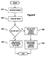
- FIG 8 a flow diagram illustrates a check performed at an input controller of Figure 2 before forwarding an inbound packet to a processing element.
- the packet is received at the input controller on a physical input (810) and the bit mask is read (820).
- a determination is made whether a bit in the mask is set (830). If a bit in the mask is set, the source is presently committed and the packet is forwarded to the processing element whose bit is set to obviate any packet ordering problem (840). If, however, no bit in the mask is set, the source is not presently committed. Accordingly, backlog information for the processing elements is referenced and the packet is forwarded to the processing element having the lowest backlog (834). Prior to such forwarding, however, the bit in the mask reserved for the selected processing element is set to commit the source to that element (832).
- a flow diagram illustrates a packet backlog update function performed at a processing element of Figure 2.
- the packet is received at a processing element from a module data bus (910).
- the source is identified (920) and the backlog count for the identified source is incremented (930).
- a flow diagram illustrates a packet backlog update and bit mask reset function performed at a processing element of Figure 2.
- the packet is retrieved from a buffer (1010) and the source is identified (1020).
- the backlog count for the identified source is decremented (1030).
- a check is made to determine if the new backlog count is zero (1040). If the new backlog count is zero, the bit mask for the identified source is reset (1050).
Abstract
Description
Claims (12)
- A method for preserving packet order integrity in a switching engine wherein packets are forwarded to different ones of a plurality of processing elements within a processor array for switching, comprising checking for each inbound packet whether another packet from the same source is pending within the processor array before forwarding the inbound packet to the processor array.
- A method for preserving packet order integrity in a switching engine wherein packets are forwarded to different ones of a plurality of parallel processing elements for switching, comprising:checking for an inbound packet whether another packet from the same source is pending at any processing element; andif another packet from the same source is pending at any processing element, forwarding the inbound packet to the processing element at which the other packet from the same source is pending.
- The method according to claim 2, further comprising:if no other packet from the same source is pending at any processing element, forwarding the inbound packet to a processing element selected in accordance with a predetermined algorithm.
- The method according to claim 2, further comprising:if no other packet from the same source is pending at any processing element, forwarding the inbound packet to a processing element selected in accordance with a predetermined load balancing algorithm.
- The method according to claim 2, further comprising:if no other packet from the same source is pending at any processing element, forwarding the inbound packet to the processing element having the lowest backlog of packets.
- A method for preserving packet order integrity in a switching engine wherein packets are forwarded to different ones of a plurality of processing elements within a processor array for switching, comprising checking for each inbound packet whether a source of the packet is committed to a processing element within the processor array before forwarding the inbound packet to the processor array.
- A method for preserving packet order integrity in a switching engine wherein packets are forwarded to different ones of a plurality of processing elements within a processor array for switching, comprising:determining if a source of an inbound packet is committed to any processing element; andif the source of the inbound packet is committed to any processing element, forwarding the inbound packet to the processing element to which the source is committed.
- The method according to claim 7, further comprising:if the source of the inbound packet is not committed to any processing element, forwarding the inbound packet to a processing element selected in accordance with a predetermined algorithm.
- The method according to claim 7, further comprising:if the source of the inbound packet is not committed to any processing element, forwarding the inbound packet to a processing element selected in accordance with a predetermined load balancing algorithm.
- The method according to claim 7, further comprising:if the source of the inbound packet is not committed to any processing element, forwarding the inbound packet to the processing element having the lowest backlog of packets.
- In a switching engine wherein packets from different sources are forwarded to different ones of a plurality of parallel processing elements for switching, a method for preserving packet order integrity, comprising:committing a source to a processing element; andforwarding inbound packets from the source to the processing element and no other processing element until the commitment is released.
- The method according to claim 11, wherein the commitment is released when all the inbound packets from the source have been switched from the processing element.
Applications Claiming Priority (2)
| Application Number | Priority Date | Filing Date | Title |
|---|---|---|---|
| US314261 | 1999-05-18 | ||
| US09/314,261 US6721309B1 (en) | 1999-05-18 | 1999-05-18 | Method and apparatus for maintaining packet order integrity in parallel switching engine |
Publications (3)
| Publication Number | Publication Date |
|---|---|
| EP1061695A2 true EP1061695A2 (en) | 2000-12-20 |
| EP1061695A3 EP1061695A3 (en) | 2004-05-19 |
| EP1061695B1 EP1061695B1 (en) | 2012-01-18 |
Family
ID=23219247
Family Applications (1)
| Application Number | Title | Priority Date | Filing Date |
|---|---|---|---|
| EP00110566A Expired - Lifetime EP1061695B1 (en) | 1999-05-18 | 2000-05-18 | Method and apparatus for maintaining packet order integrity in a parallel switching engine |
Country Status (4)
| Country | Link |
|---|---|
| US (1) | US6721309B1 (en) |
| EP (1) | EP1061695B1 (en) |
| JP (1) | JP3394504B2 (en) |
| AT (1) | ATE542335T1 (en) |
Cited By (5)
| Publication number | Priority date | Publication date | Assignee | Title |
|---|---|---|---|---|
| EP1326400A2 (en) * | 2001-12-21 | 2003-07-09 | Agere Systems Inc. | Processor with packet processing order maintenance based on packet flow identifiers |
| EP1531589A2 (en) * | 2003-11-13 | 2005-05-18 | Arteris | System and method for transmission of a message sequence in an interconnection network |
| US7574629B2 (en) | 2004-03-02 | 2009-08-11 | Arteris | Method and device for switching between agents |
| US7769027B2 (en) | 2003-08-13 | 2010-08-03 | Arteris | Method and device for managing priority during the transmission of a message |
| EP2670099A1 (en) * | 2012-05-31 | 2013-12-04 | Hitachi Ltd. | Communication apparatus and communication method |
Families Citing this family (16)
| Publication number | Priority date | Publication date | Assignee | Title |
|---|---|---|---|---|
| DE10011667C2 (en) * | 2000-03-10 | 2002-11-21 | Infineon Technologies Ag | High Speed Router |
| WO2002093828A2 (en) * | 2001-05-17 | 2002-11-21 | Solidum Systems Corporation | Distributed packet processing system with internal load distribution |
| FR2890766B1 (en) * | 2005-09-12 | 2007-11-30 | Arteris Sa | SYSTEM AND METHOD FOR ASYNCHRONOUS CIRCUIT COMMUNICATION BETWEEN SYNCHRONOUS SUB-CIRCUITS |
| FR2899413B1 (en) * | 2006-03-31 | 2008-08-08 | Arteris Sa | MESSAGE SWITCHING SYSTEM |
| FR2900017B1 (en) * | 2006-04-12 | 2008-10-31 | Arteris Sa | EXTERNAL CHIP FUNCTIONAL BLOCK INTERCONNECTION SYSTEM PROVIDED WITH A SINGLE COMMUNICATION PARAMETRABLE PROTOCOL |
| FR2901437B1 (en) * | 2006-05-16 | 2008-08-08 | Arteris Sa | METHOD FOR MAKING A SYNCHRONIZATION CIRCUIT OF ASYNCHRONOUSLY EXCHANGED DATA BETWEEN TWO SYNCHRONOUS BLOCKS, AND SYNCHRONIZATION CIRCUIT PRODUCED BY SUCH A METHOD |
| FR2902957B1 (en) * | 2006-06-23 | 2008-09-12 | Arteris Sa | SYSTEM AND METHOD FOR MANAGING MESSAGES TRANSMITTED IN AN INTERCONNECTION NETWORK |
| FR2904445B1 (en) * | 2006-07-26 | 2008-10-10 | Arteris Sa | SYSTEM FOR MANAGING MESSAGES TRANSMITTED IN A CHIP INTERCONNECTION NETWORK |
| US9286118B2 (en) * | 2012-06-15 | 2016-03-15 | Freescale Semiconductor, Inc. | System and method for improved job processing to reduce contention for shared resources |
| US9104478B2 (en) | 2012-06-15 | 2015-08-11 | Freescale Semiconductor, Inc. | System and method for improved job processing of a number of jobs belonging to communication streams within a data processor |
| US8842675B2 (en) | 2012-08-23 | 2014-09-23 | L-3 Communications Corporation | Systems and methods for multicore processing of data with in-sequence delivery |
| US9632977B2 (en) | 2013-03-13 | 2017-04-25 | Nxp Usa, Inc. | System and method for ordering packet transfers in a data processor |
| US9372723B2 (en) | 2014-04-01 | 2016-06-21 | Freescale Semiconductor, Inc. | System and method for conditional task switching during ordering scope transitions |
| US9372724B2 (en) | 2014-04-01 | 2016-06-21 | Freescale Semiconductor, Inc. | System and method for conditional task switching during ordering scope transitions |
| US9733981B2 (en) | 2014-06-10 | 2017-08-15 | Nxp Usa, Inc. | System and method for conditional task switching during ordering scope transitions |
| US11169845B2 (en) * | 2017-12-21 | 2021-11-09 | Ciena Corporation | Flow and application based processor scheduling for network functions virtualization applications using flow identification based on logical calculations on frame based fields |
Citations (2)
| Publication number | Priority date | Publication date | Assignee | Title |
|---|---|---|---|---|
| US4598400A (en) * | 1983-05-31 | 1986-07-01 | Thinking Machines Corporation | Method and apparatus for routing message packets |
| EP0375249A2 (en) * | 1988-12-21 | 1990-06-27 | AT&T Corp. | Self routing packet switching network architecture |
Family Cites Families (8)
| Publication number | Priority date | Publication date | Assignee | Title |
|---|---|---|---|---|
| BE905982A (en) | 1986-12-19 | 1987-06-19 | Electronique Et Telecomm Bell | PACKET SWITCHING NETWORK. |
| US5127001A (en) * | 1990-06-22 | 1992-06-30 | Unisys Corporation | Conference call arrangement for distributed network |
| US5889764A (en) * | 1995-08-31 | 1999-03-30 | Intel Corporation | Low-latency multi-party audio chat |
| US5793747A (en) * | 1996-03-14 | 1998-08-11 | Motorola, Inc. | Event-driven cell scheduler and method for supporting multiple service categories in a communication network |
| US6452933B1 (en) * | 1997-02-07 | 2002-09-17 | Lucent Technologies Inc. | Fair queuing system with adaptive bandwidth redistribution |
| US6092115A (en) * | 1997-02-07 | 2000-07-18 | Lucent Technologies Inc. | Method for supporting per-connection queuing for feedback-controlled traffic |
| US5864540A (en) * | 1997-04-04 | 1999-01-26 | At&T Corp/Csi Zeinet(A Cabletron Co.) | Method for integrated traffic shaping in a packet-switched network |
| KR100233091B1 (en) * | 1997-10-23 | 1999-12-01 | 윤종용 | Atm traffic control apparatus and method |
-
1999
- 1999-05-18 US US09/314,261 patent/US6721309B1/en not_active Expired - Lifetime
-
2000
- 2000-05-16 JP JP2000142912A patent/JP3394504B2/en not_active Expired - Fee Related
- 2000-05-18 EP EP00110566A patent/EP1061695B1/en not_active Expired - Lifetime
- 2000-05-18 AT AT00110566T patent/ATE542335T1/en active
Patent Citations (2)
| Publication number | Priority date | Publication date | Assignee | Title |
|---|---|---|---|---|
| US4598400A (en) * | 1983-05-31 | 1986-07-01 | Thinking Machines Corporation | Method and apparatus for routing message packets |
| EP0375249A2 (en) * | 1988-12-21 | 1990-06-27 | AT&T Corp. | Self routing packet switching network architecture |
Non-Patent Citations (1)
| Title |
|---|
| KOLIAS C ET AL: "PERFORMANCE ANALYSIS OF MULTIPLANE, NONBLOCKING ATM SWITCHES" IEEE GLOBECOM 1998. GLOBECOM '98. THE BRIDGE TO GLOBAL INTEGRATION. SYDNEY, NOV. 8 - 12, 1998, IEEE GLOBAL TELECOMMUNICATIONS CONFERENCE, NEW YORK, NY: IEEE, US, vol. 1, 8 November 1998 (1998-11-08), pages 356-362, XP000894329 ISBN: 0-7803-4985-7 * |
Cited By (14)
| Publication number | Priority date | Publication date | Assignee | Title |
|---|---|---|---|---|
| JP2009081897A (en) * | 2001-12-21 | 2009-04-16 | Agere Systems Inc | Processor maintaining sequence of packet processing on the basis of packet flow identifiers |
| EP1326400A3 (en) * | 2001-12-21 | 2004-03-24 | Agere Systems Inc. | Processor with packet processing order maintenance based on packet flow identifiers |
| EP1326400A2 (en) * | 2001-12-21 | 2003-07-09 | Agere Systems Inc. | Processor with packet processing order maintenance based on packet flow identifiers |
| KR100945103B1 (en) | 2001-12-21 | 2010-03-02 | 에이저 시스템즈 인크 | Processor with packet processing order maintenance based on packet flow identifiers |
| US7088719B2 (en) | 2001-12-21 | 2006-08-08 | Agere Systems Inc. | Processor with packet processing order maintenance based on packet flow identifiers |
| US7769027B2 (en) | 2003-08-13 | 2010-08-03 | Arteris | Method and device for managing priority during the transmission of a message |
| US8441931B2 (en) | 2003-08-13 | 2013-05-14 | Arteris Inc. | Method and device for managing priority during the transmission of a message |
| US9172656B2 (en) | 2003-08-13 | 2015-10-27 | Qualcomm Technologies, Inc. | Method and device for managing priority during the transmission of a message |
| EP1531589A3 (en) * | 2003-11-13 | 2007-05-23 | Arteris | System and method for transmission of a message sequence in an interconnection network |
| FR2862457A1 (en) * | 2003-11-13 | 2005-05-20 | Arteris | SYSTEM AND METHOD FOR TRANSMITTING A SEQUENCE OF MESSAGES IN AN INTERCONNECTION NETWORK. |
| EP1531589A2 (en) * | 2003-11-13 | 2005-05-18 | Arteris | System and method for transmission of a message sequence in an interconnection network |
| US8031730B2 (en) | 2003-11-13 | 2011-10-04 | Arteris | System and method for transmitting a sequence of messages in an interconnection network |
| US7574629B2 (en) | 2004-03-02 | 2009-08-11 | Arteris | Method and device for switching between agents |
| EP2670099A1 (en) * | 2012-05-31 | 2013-12-04 | Hitachi Ltd. | Communication apparatus and communication method |
Also Published As
| Publication number | Publication date |
|---|---|
| US6721309B1 (en) | 2004-04-13 |
| EP1061695A3 (en) | 2004-05-19 |
| EP1061695B1 (en) | 2012-01-18 |
| ATE542335T1 (en) | 2012-02-15 |
| JP2000358066A (en) | 2000-12-26 |
| JP3394504B2 (en) | 2003-04-07 |
Similar Documents
| Publication | Publication Date | Title |
|---|---|---|
| US6721309B1 (en) | Method and apparatus for maintaining packet order integrity in parallel switching engine | |
| US6947433B2 (en) | System and method for implementing source based and egress based virtual networks in an interconnection network | |
| US7319669B1 (en) | Method and system for controlling packet flow in networks | |
| US7039058B2 (en) | Switched interconnection network with increased bandwidth and port count | |
| US9817773B2 (en) | System and method for preserving order of data processed by processing engines | |
| US7046633B2 (en) | Router implemented with a gamma graph interconnection network | |
| WO2020236290A1 (en) | System and method for facilitating efficient address translation in a network interface controller (nic) | |
| US7814283B1 (en) | Low latency request dispatcher | |
| EP1421739B1 (en) | Transmitting multicast data packets | |
| US7391772B2 (en) | Network multicasting | |
| JP4024904B2 (en) | Data unit for receiving a data packet and distributing it to a packet switching circuit, and an exchange including the data unit | |
| US7733889B2 (en) | Network switching device and method dividing packets and storing divided packets in shared buffer | |
| US5418781A (en) | Architecture for maintaining the sequence of packet cells transmitted over a multicast, cell-switched network | |
| US6219352B1 (en) | Queue management with support for multicasts in an asynchronous transfer mode (ATM) switch | |
| WO1999040754A1 (en) | Arbitration method and apparatus for a non-blocking switch | |
| JP3946145B2 (en) | Fast Ethernet switch and method for distributing Fast Ethernet data frames | |
| KR20030080027A (en) | Switching arrangement and method with separated output buffers | |
| US8996724B2 (en) | Context switched route look up key engine | |
| US7174394B1 (en) | Multi processor enqueue packet circuit | |
| US8520675B1 (en) | System and method for efficient packet replication | |
| US6643294B1 (en) | Distributed control merged buffer ATM switch | |
| US20140185629A1 (en) | Queue processing method | |
| JP2002057719A (en) | Method and system for packet re-assembling in communication switch | |
| US20020176424A1 (en) | System and method for switching asynchronous transfer mode cells | |
| US20050036445A1 (en) | Processing data packets |
Legal Events
| Date | Code | Title | Description |
|---|---|---|---|
| PUAI | Public reference made under article 153(3) epc to a published international application that has entered the european phase |
Free format text: ORIGINAL CODE: 0009012 |
|
| AK | Designated contracting states |
Kind code of ref document: A2 Designated state(s): AT BE CH CY DE DK ES FI FR GB GR IE IT LI LU MC NL PT SE |
|
| AX | Request for extension of the european patent |
Free format text: AL;LT;LV;MK;RO;SI |
|
| PUAL | Search report despatched |
Free format text: ORIGINAL CODE: 0009013 |
|
| AK | Designated contracting states |
Kind code of ref document: A3 Designated state(s): AT BE CH CY DE DK ES FI FR GB GR IE IT LI LU MC NL PT SE |
|
| AX | Request for extension of the european patent |
Extension state: AL LT LV MK RO SI |
|
| 17P | Request for examination filed |
Effective date: 20041116 |
|
| AKX | Designation fees paid |
Designated state(s): AT BE CH CY DE DK ES FI FR GB GR IE IT LI LU MC NL PT SE |
|
| 17Q | First examination report despatched |
Effective date: 20050117 |
|
| GRAP | Despatch of communication of intention to grant a patent |
Free format text: ORIGINAL CODE: EPIDOSNIGR1 |
|
| GRAS | Grant fee paid |
Free format text: ORIGINAL CODE: EPIDOSNIGR3 |
|
| GRAA | (expected) grant |
Free format text: ORIGINAL CODE: 0009210 |
|
| RAP1 | Party data changed (applicant data changed or rights of an application transferred) |
Owner name: ALCATEL LUCENT |
|
| AK | Designated contracting states |
Kind code of ref document: B1 Designated state(s): AT BE CH CY DE DK ES FI FR GB GR IE IT LI LU MC NL PT SE |
|
| REG | Reference to a national code |
Ref country code: GB Ref legal event code: FG4D |
|
| REG | Reference to a national code |
Ref country code: CH Ref legal event code: EP |
|
| REG | Reference to a national code |
Ref country code: IE Ref legal event code: FG4D Ref country code: AT Ref legal event code: REF Ref document number: 542335 Country of ref document: AT Kind code of ref document: T Effective date: 20120215 |
|
| REG | Reference to a national code |
Ref country code: DE Ref legal event code: R096 Ref document number: 60046843 Country of ref document: DE Effective date: 20120315 |
|
| REG | Reference to a national code |
Ref country code: NL Ref legal event code: VDEP Effective date: 20120118 |
|
| PG25 | Lapsed in a contracting state [announced via postgrant information from national office to epo] |
Ref country code: BE Free format text: LAPSE BECAUSE OF FAILURE TO SUBMIT A TRANSLATION OF THE DESCRIPTION OR TO PAY THE FEE WITHIN THE PRESCRIBED TIME-LIMIT Effective date: 20120118 Ref country code: NL Free format text: LAPSE BECAUSE OF FAILURE TO SUBMIT A TRANSLATION OF THE DESCRIPTION OR TO PAY THE FEE WITHIN THE PRESCRIBED TIME-LIMIT Effective date: 20120118 |
|
| PG25 | Lapsed in a contracting state [announced via postgrant information from national office to epo] |
Ref country code: PT Free format text: LAPSE BECAUSE OF FAILURE TO SUBMIT A TRANSLATION OF THE DESCRIPTION OR TO PAY THE FEE WITHIN THE PRESCRIBED TIME-LIMIT Effective date: 20120518 Ref country code: FI Free format text: LAPSE BECAUSE OF FAILURE TO SUBMIT A TRANSLATION OF THE DESCRIPTION OR TO PAY THE FEE WITHIN THE PRESCRIBED TIME-LIMIT Effective date: 20120118 Ref country code: GR Free format text: LAPSE BECAUSE OF FAILURE TO SUBMIT A TRANSLATION OF THE DESCRIPTION OR TO PAY THE FEE WITHIN THE PRESCRIBED TIME-LIMIT Effective date: 20120419 |
|
| REG | Reference to a national code |
Ref country code: AT Ref legal event code: MK05 Ref document number: 542335 Country of ref document: AT Kind code of ref document: T Effective date: 20120118 |
|
| PG25 | Lapsed in a contracting state [announced via postgrant information from national office to epo] |
Ref country code: CY Free format text: LAPSE BECAUSE OF FAILURE TO SUBMIT A TRANSLATION OF THE DESCRIPTION OR TO PAY THE FEE WITHIN THE PRESCRIBED TIME-LIMIT Effective date: 20120118 |
|
| PG25 | Lapsed in a contracting state [announced via postgrant information from national office to epo] |
Ref country code: SE Free format text: LAPSE BECAUSE OF FAILURE TO SUBMIT A TRANSLATION OF THE DESCRIPTION OR TO PAY THE FEE WITHIN THE PRESCRIBED TIME-LIMIT Effective date: 20120118 Ref country code: DK Free format text: LAPSE BECAUSE OF FAILURE TO SUBMIT A TRANSLATION OF THE DESCRIPTION OR TO PAY THE FEE WITHIN THE PRESCRIBED TIME-LIMIT Effective date: 20120118 |
|
| PLBE | No opposition filed within time limit |
Free format text: ORIGINAL CODE: 0009261 |
|
| STAA | Information on the status of an ep patent application or granted ep patent |
Free format text: STATUS: NO OPPOSITION FILED WITHIN TIME LIMIT |
|
| PG25 | Lapsed in a contracting state [announced via postgrant information from national office to epo] |
Ref country code: IT Free format text: LAPSE BECAUSE OF FAILURE TO SUBMIT A TRANSLATION OF THE DESCRIPTION OR TO PAY THE FEE WITHIN THE PRESCRIBED TIME-LIMIT Effective date: 20120118 |
|
| 26N | No opposition filed |
Effective date: 20121019 |
|
| PG25 | Lapsed in a contracting state [announced via postgrant information from national office to epo] |
Ref country code: MC Free format text: LAPSE BECAUSE OF NON-PAYMENT OF DUE FEES Effective date: 20120531 |
|
| REG | Reference to a national code |
Ref country code: CH Ref legal event code: PL |
|
| PG25 | Lapsed in a contracting state [announced via postgrant information from national office to epo] |
Ref country code: CH Free format text: LAPSE BECAUSE OF NON-PAYMENT OF DUE FEES Effective date: 20120531 Ref country code: AT Free format text: LAPSE BECAUSE OF FAILURE TO SUBMIT A TRANSLATION OF THE DESCRIPTION OR TO PAY THE FEE WITHIN THE PRESCRIBED TIME-LIMIT Effective date: 20120118 Ref country code: LI Free format text: LAPSE BECAUSE OF NON-PAYMENT OF DUE FEES Effective date: 20120531 |
|
| REG | Reference to a national code |
Ref country code: DE Ref legal event code: R097 Ref document number: 60046843 Country of ref document: DE Effective date: 20121019 |
|
| REG | Reference to a national code |
Ref country code: IE Ref legal event code: MM4A |
|
| PG25 | Lapsed in a contracting state [announced via postgrant information from national office to epo] |
Ref country code: ES Free format text: LAPSE BECAUSE OF FAILURE TO SUBMIT A TRANSLATION OF THE DESCRIPTION OR TO PAY THE FEE WITHIN THE PRESCRIBED TIME-LIMIT Effective date: 20120429 Ref country code: IE Free format text: LAPSE BECAUSE OF NON-PAYMENT OF DUE FEES Effective date: 20120518 |
|
| REG | Reference to a national code |
Ref country code: GB Ref legal event code: 732E Free format text: REGISTERED BETWEEN 20130926 AND 20131002 |
|
| REG | Reference to a national code |
Ref country code: FR Ref legal event code: GC Effective date: 20131018 |
|
| PG25 | Lapsed in a contracting state [announced via postgrant information from national office to epo] |
Ref country code: LU Free format text: LAPSE BECAUSE OF NON-PAYMENT OF DUE FEES Effective date: 20120518 |
|
| REG | Reference to a national code |
Ref country code: FR Ref legal event code: RG Effective date: 20141016 |
|
| REG | Reference to a national code |
Ref country code: FR Ref legal event code: PLFP Year of fee payment: 16 |
|
| REG | Reference to a national code |
Ref country code: FR Ref legal event code: PLFP Year of fee payment: 17 |
|
| PGFP | Annual fee paid to national office [announced via postgrant information from national office to epo] |
Ref country code: GB Payment date: 20160520 Year of fee payment: 17 Ref country code: DE Payment date: 20160520 Year of fee payment: 17 |
|
| PGFP | Annual fee paid to national office [announced via postgrant information from national office to epo] |
Ref country code: FR Payment date: 20160520 Year of fee payment: 17 |
|
| REG | Reference to a national code |
Ref country code: DE Ref legal event code: R119 Ref document number: 60046843 Country of ref document: DE |
|
| GBPC | Gb: european patent ceased through non-payment of renewal fee |
Effective date: 20170518 |
|
| REG | Reference to a national code |
Ref country code: FR Ref legal event code: ST Effective date: 20180131 |
|
| PG25 | Lapsed in a contracting state [announced via postgrant information from national office to epo] |
Ref country code: DE Free format text: LAPSE BECAUSE OF NON-PAYMENT OF DUE FEES Effective date: 20171201 Ref country code: GB Free format text: LAPSE BECAUSE OF NON-PAYMENT OF DUE FEES Effective date: 20170518 |
|
| PG25 | Lapsed in a contracting state [announced via postgrant information from national office to epo] |
Ref country code: FR Free format text: LAPSE BECAUSE OF NON-PAYMENT OF DUE FEES Effective date: 20170531 |