EP1060892A2 - Ink chamber and orifice shape variations in an ink-jet orifice plate - Google Patents
Ink chamber and orifice shape variations in an ink-jet orifice plate Download PDFInfo
- Publication number
- EP1060892A2 EP1060892A2 EP00304403A EP00304403A EP1060892A2 EP 1060892 A2 EP1060892 A2 EP 1060892A2 EP 00304403 A EP00304403 A EP 00304403A EP 00304403 A EP00304403 A EP 00304403A EP 1060892 A2 EP1060892 A2 EP 1060892A2
- Authority
- EP
- European Patent Office
- Prior art keywords
- ink
- layer
- chamber
- depth
- orifice plate
- Prior art date
- Legal status (The legal status is an assumption and is not a legal conclusion. Google has not performed a legal analysis and makes no representation as to the accuracy of the status listed.)
- Granted
Links
- 238000000034 method Methods 0.000 claims abstract description 6
- 230000005855 radiation Effects 0.000 claims description 20
- 239000000758 substrate Substances 0.000 claims description 14
- 229920002120 photoresistant polymer Polymers 0.000 claims description 13
- 239000000463 material Substances 0.000 claims description 11
- 230000005670 electromagnetic radiation Effects 0.000 claims description 3
- 238000004519 manufacturing process Methods 0.000 claims description 3
- 239000000976 ink Substances 0.000 description 60
- 239000010410 layer Substances 0.000 description 39
- 238000004132 cross linking Methods 0.000 description 9
- 238000013461 design Methods 0.000 description 8
- 230000000903 blocking effect Effects 0.000 description 6
- 230000004888 barrier function Effects 0.000 description 5
- VYPSYNLAJGMNEJ-UHFFFAOYSA-N Silicium dioxide Chemical compound O=[Si]=O VYPSYNLAJGMNEJ-UHFFFAOYSA-N 0.000 description 4
- XUIMIQQOPSSXEZ-UHFFFAOYSA-N Silicon Chemical compound [Si] XUIMIQQOPSSXEZ-UHFFFAOYSA-N 0.000 description 4
- 229910052710 silicon Inorganic materials 0.000 description 4
- 239000010703 silicon Substances 0.000 description 4
- 239000003086 colorant Substances 0.000 description 3
- VYZAMTAEIAYCRO-UHFFFAOYSA-N Chromium Chemical compound [Cr] VYZAMTAEIAYCRO-UHFFFAOYSA-N 0.000 description 2
- PXHVJJICTQNCMI-UHFFFAOYSA-N Nickel Chemical compound [Ni] PXHVJJICTQNCMI-UHFFFAOYSA-N 0.000 description 2
- 239000011651 chromium Substances 0.000 description 2
- 238000004891 communication Methods 0.000 description 2
- 238000010586 diagram Methods 0.000 description 2
- 239000012530 fluid Substances 0.000 description 2
- 238000009413 insulation Methods 0.000 description 2
- 238000002161 passivation Methods 0.000 description 2
- 230000035515 penetration Effects 0.000 description 2
- 235000012239 silicon dioxide Nutrition 0.000 description 2
- 239000000377 silicon dioxide Substances 0.000 description 2
- 210000004894 snout Anatomy 0.000 description 2
- 229910000599 Cr alloy Inorganic materials 0.000 description 1
- 229910000640 Fe alloy Inorganic materials 0.000 description 1
- 229910000990 Ni alloy Inorganic materials 0.000 description 1
- RVSGESPTHDDNTH-UHFFFAOYSA-N alumane;tantalum Chemical compound [AlH3].[Ta] RVSGESPTHDDNTH-UHFFFAOYSA-N 0.000 description 1
- 229910052804 chromium Inorganic materials 0.000 description 1
- 239000004020 conductor Substances 0.000 description 1
- 238000011161 development Methods 0.000 description 1
- 239000003822 epoxy resin Substances 0.000 description 1
- 239000010408 film Substances 0.000 description 1
- 238000010438 heat treatment Methods 0.000 description 1
- 229910001026 inconel Inorganic materials 0.000 description 1
- 239000007788 liquid Substances 0.000 description 1
- 238000012986 modification Methods 0.000 description 1
- 230000004048 modification Effects 0.000 description 1
- 239000004033 plastic Substances 0.000 description 1
- 229920000647 polyepoxide Polymers 0.000 description 1
- 238000012545 processing Methods 0.000 description 1
- 229910052709 silver Inorganic materials 0.000 description 1
- 239000004332 silver Substances 0.000 description 1
- 239000002356 single layer Substances 0.000 description 1
- 239000010409 thin film Substances 0.000 description 1
Images
Classifications
-
- B—PERFORMING OPERATIONS; TRANSPORTING
- B41—PRINTING; LINING MACHINES; TYPEWRITERS; STAMPS
- B41J—TYPEWRITERS; SELECTIVE PRINTING MECHANISMS, i.e. MECHANISMS PRINTING OTHERWISE THAN FROM A FORME; CORRECTION OF TYPOGRAPHICAL ERRORS
- B41J2/00—Typewriters or selective printing mechanisms characterised by the printing or marking process for which they are designed
- B41J2/005—Typewriters or selective printing mechanisms characterised by the printing or marking process for which they are designed characterised by bringing liquid or particles selectively into contact with a printing material
- B41J2/01—Ink jet
- B41J2/135—Nozzles
- B41J2/14—Structure thereof only for on-demand ink jet heads
- B41J2/14016—Structure of bubble jet print heads
- B41J2/14072—Electrical connections, e.g. details on electrodes, connecting the chip to the outside...
-
- B—PERFORMING OPERATIONS; TRANSPORTING
- B41—PRINTING; LINING MACHINES; TYPEWRITERS; STAMPS
- B41J—TYPEWRITERS; SELECTIVE PRINTING MECHANISMS, i.e. MECHANISMS PRINTING OTHERWISE THAN FROM A FORME; CORRECTION OF TYPOGRAPHICAL ERRORS
- B41J2/00—Typewriters or selective printing mechanisms characterised by the printing or marking process for which they are designed
- B41J2/005—Typewriters or selective printing mechanisms characterised by the printing or marking process for which they are designed characterised by bringing liquid or particles selectively into contact with a printing material
- B41J2/01—Ink jet
- B41J2/135—Nozzles
- B41J2/14—Structure thereof only for on-demand ink jet heads
- B41J2/14016—Structure of bubble jet print heads
- B41J2/14032—Structure of the pressure chamber
- B41J2/1404—Geometrical characteristics
-
- B—PERFORMING OPERATIONS; TRANSPORTING
- B41—PRINTING; LINING MACHINES; TYPEWRITERS; STAMPS
- B41J—TYPEWRITERS; SELECTIVE PRINTING MECHANISMS, i.e. MECHANISMS PRINTING OTHERWISE THAN FROM A FORME; CORRECTION OF TYPOGRAPHICAL ERRORS
- B41J2/00—Typewriters or selective printing mechanisms characterised by the printing or marking process for which they are designed
- B41J2/005—Typewriters or selective printing mechanisms characterised by the printing or marking process for which they are designed characterised by bringing liquid or particles selectively into contact with a printing material
- B41J2/01—Ink jet
- B41J2/135—Nozzles
- B41J2/14—Structure thereof only for on-demand ink jet heads
- B41J2/14016—Structure of bubble jet print heads
- B41J2/1408—Structure dealing with thermal variations, e.g. cooling device, thermal coefficients of materials
-
- B—PERFORMING OPERATIONS; TRANSPORTING
- B41—PRINTING; LINING MACHINES; TYPEWRITERS; STAMPS
- B41J—TYPEWRITERS; SELECTIVE PRINTING MECHANISMS, i.e. MECHANISMS PRINTING OTHERWISE THAN FROM A FORME; CORRECTION OF TYPOGRAPHICAL ERRORS
- B41J2/00—Typewriters or selective printing mechanisms characterised by the printing or marking process for which they are designed
- B41J2/005—Typewriters or selective printing mechanisms characterised by the printing or marking process for which they are designed characterised by bringing liquid or particles selectively into contact with a printing material
- B41J2/01—Ink jet
- B41J2/135—Nozzles
- B41J2/14—Structure thereof only for on-demand ink jet heads
- B41J2/14016—Structure of bubble jet print heads
- B41J2/14088—Structure of heating means
- B41J2/14112—Resistive element
- B41J2/14129—Layer structure
-
- B—PERFORMING OPERATIONS; TRANSPORTING
- B41—PRINTING; LINING MACHINES; TYPEWRITERS; STAMPS
- B41J—TYPEWRITERS; SELECTIVE PRINTING MECHANISMS, i.e. MECHANISMS PRINTING OTHERWISE THAN FROM A FORME; CORRECTION OF TYPOGRAPHICAL ERRORS
- B41J2/00—Typewriters or selective printing mechanisms characterised by the printing or marking process for which they are designed
- B41J2/005—Typewriters or selective printing mechanisms characterised by the printing or marking process for which they are designed characterised by bringing liquid or particles selectively into contact with a printing material
- B41J2/01—Ink jet
- B41J2/135—Nozzles
- B41J2/14—Structure thereof only for on-demand ink jet heads
- B41J2/1433—Structure of nozzle plates
-
- B—PERFORMING OPERATIONS; TRANSPORTING
- B41—PRINTING; LINING MACHINES; TYPEWRITERS; STAMPS
- B41J—TYPEWRITERS; SELECTIVE PRINTING MECHANISMS, i.e. MECHANISMS PRINTING OTHERWISE THAN FROM A FORME; CORRECTION OF TYPOGRAPHICAL ERRORS
- B41J2/00—Typewriters or selective printing mechanisms characterised by the printing or marking process for which they are designed
- B41J2/005—Typewriters or selective printing mechanisms characterised by the printing or marking process for which they are designed characterised by bringing liquid or particles selectively into contact with a printing material
- B41J2/01—Ink jet
- B41J2/135—Nozzles
- B41J2/16—Production of nozzles
- B41J2/1601—Production of bubble jet print heads
- B41J2/1603—Production of bubble jet print heads of the front shooter type
-
- B—PERFORMING OPERATIONS; TRANSPORTING
- B41—PRINTING; LINING MACHINES; TYPEWRITERS; STAMPS
- B41J—TYPEWRITERS; SELECTIVE PRINTING MECHANISMS, i.e. MECHANISMS PRINTING OTHERWISE THAN FROM A FORME; CORRECTION OF TYPOGRAPHICAL ERRORS
- B41J2/00—Typewriters or selective printing mechanisms characterised by the printing or marking process for which they are designed
- B41J2/005—Typewriters or selective printing mechanisms characterised by the printing or marking process for which they are designed characterised by bringing liquid or particles selectively into contact with a printing material
- B41J2/01—Ink jet
- B41J2/135—Nozzles
- B41J2/16—Production of nozzles
- B41J2/162—Manufacturing of the nozzle plates
-
- B—PERFORMING OPERATIONS; TRANSPORTING
- B41—PRINTING; LINING MACHINES; TYPEWRITERS; STAMPS
- B41J—TYPEWRITERS; SELECTIVE PRINTING MECHANISMS, i.e. MECHANISMS PRINTING OTHERWISE THAN FROM A FORME; CORRECTION OF TYPOGRAPHICAL ERRORS
- B41J2/00—Typewriters or selective printing mechanisms characterised by the printing or marking process for which they are designed
- B41J2/005—Typewriters or selective printing mechanisms characterised by the printing or marking process for which they are designed characterised by bringing liquid or particles selectively into contact with a printing material
- B41J2/01—Ink jet
- B41J2/135—Nozzles
- B41J2/16—Production of nozzles
- B41J2/1621—Manufacturing processes
- B41J2/1626—Manufacturing processes etching
- B41J2/1628—Manufacturing processes etching dry etching
-
- B—PERFORMING OPERATIONS; TRANSPORTING
- B41—PRINTING; LINING MACHINES; TYPEWRITERS; STAMPS
- B41J—TYPEWRITERS; SELECTIVE PRINTING MECHANISMS, i.e. MECHANISMS PRINTING OTHERWISE THAN FROM A FORME; CORRECTION OF TYPOGRAPHICAL ERRORS
- B41J2/00—Typewriters or selective printing mechanisms characterised by the printing or marking process for which they are designed
- B41J2/005—Typewriters or selective printing mechanisms characterised by the printing or marking process for which they are designed characterised by bringing liquid or particles selectively into contact with a printing material
- B41J2/01—Ink jet
- B41J2/135—Nozzles
- B41J2/16—Production of nozzles
- B41J2/1621—Manufacturing processes
- B41J2/1626—Manufacturing processes etching
- B41J2/1629—Manufacturing processes etching wet etching
-
- B—PERFORMING OPERATIONS; TRANSPORTING
- B41—PRINTING; LINING MACHINES; TYPEWRITERS; STAMPS
- B41J—TYPEWRITERS; SELECTIVE PRINTING MECHANISMS, i.e. MECHANISMS PRINTING OTHERWISE THAN FROM A FORME; CORRECTION OF TYPOGRAPHICAL ERRORS
- B41J2/00—Typewriters or selective printing mechanisms characterised by the printing or marking process for which they are designed
- B41J2/005—Typewriters or selective printing mechanisms characterised by the printing or marking process for which they are designed characterised by bringing liquid or particles selectively into contact with a printing material
- B41J2/01—Ink jet
- B41J2/135—Nozzles
- B41J2/16—Production of nozzles
- B41J2/1621—Manufacturing processes
- B41J2/1631—Manufacturing processes photolithography
-
- B—PERFORMING OPERATIONS; TRANSPORTING
- B41—PRINTING; LINING MACHINES; TYPEWRITERS; STAMPS
- B41J—TYPEWRITERS; SELECTIVE PRINTING MECHANISMS, i.e. MECHANISMS PRINTING OTHERWISE THAN FROM A FORME; CORRECTION OF TYPOGRAPHICAL ERRORS
- B41J2/00—Typewriters or selective printing mechanisms characterised by the printing or marking process for which they are designed
- B41J2/005—Typewriters or selective printing mechanisms characterised by the printing or marking process for which they are designed characterised by bringing liquid or particles selectively into contact with a printing material
- B41J2/01—Ink jet
- B41J2/135—Nozzles
- B41J2/16—Production of nozzles
- B41J2/1621—Manufacturing processes
- B41J2/1637—Manufacturing processes molding
- B41J2/1639—Manufacturing processes molding sacrificial molding
-
- B—PERFORMING OPERATIONS; TRANSPORTING
- B41—PRINTING; LINING MACHINES; TYPEWRITERS; STAMPS
- B41J—TYPEWRITERS; SELECTIVE PRINTING MECHANISMS, i.e. MECHANISMS PRINTING OTHERWISE THAN FROM A FORME; CORRECTION OF TYPOGRAPHICAL ERRORS
- B41J2/00—Typewriters or selective printing mechanisms characterised by the printing or marking process for which they are designed
- B41J2/005—Typewriters or selective printing mechanisms characterised by the printing or marking process for which they are designed characterised by bringing liquid or particles selectively into contact with a printing material
- B41J2/01—Ink jet
- B41J2/135—Nozzles
- B41J2/16—Production of nozzles
- B41J2/1621—Manufacturing processes
- B41J2/164—Manufacturing processes thin film formation
- B41J2/1645—Manufacturing processes thin film formation thin film formation by spincoating
-
- B—PERFORMING OPERATIONS; TRANSPORTING
- B41—PRINTING; LINING MACHINES; TYPEWRITERS; STAMPS
- B41J—TYPEWRITERS; SELECTIVE PRINTING MECHANISMS, i.e. MECHANISMS PRINTING OTHERWISE THAN FROM A FORME; CORRECTION OF TYPOGRAPHICAL ERRORS
- B41J2/00—Typewriters or selective printing mechanisms characterised by the printing or marking process for which they are designed
- B41J2/005—Typewriters or selective printing mechanisms characterised by the printing or marking process for which they are designed characterised by bringing liquid or particles selectively into contact with a printing material
- B41J2/01—Ink jet
- B41J2/135—Nozzles
- B41J2/14—Structure thereof only for on-demand ink jet heads
- B41J2002/14387—Front shooter
-
- B—PERFORMING OPERATIONS; TRANSPORTING
- B41—PRINTING; LINING MACHINES; TYPEWRITERS; STAMPS
- B41J—TYPEWRITERS; SELECTIVE PRINTING MECHANISMS, i.e. MECHANISMS PRINTING OTHERWISE THAN FROM A FORME; CORRECTION OF TYPOGRAPHICAL ERRORS
- B41J2/00—Typewriters or selective printing mechanisms characterised by the printing or marking process for which they are designed
- B41J2/005—Typewriters or selective printing mechanisms characterised by the printing or marking process for which they are designed characterised by bringing liquid or particles selectively into contact with a printing material
- B41J2/01—Ink jet
- B41J2/135—Nozzles
- B41J2/14—Structure thereof only for on-demand ink jet heads
- B41J2002/14475—Structure thereof only for on-demand ink jet heads characterised by nozzle shapes or number of orifices per chamber
Landscapes
- Engineering & Computer Science (AREA)
- Manufacturing & Machinery (AREA)
- Physics & Mathematics (AREA)
- Geometry (AREA)
- Thermal Sciences (AREA)
- Particle Formation And Scattering Control In Inkjet Printers (AREA)
Abstract
Description
- This invention relates to ink-jet printers, and particularly to orifice plates that are incorporated into the print heads of ink cartridges used in those printers.
- An ink-jet printer includes one or more ink cartridges that contain ink. In some designs, the cartridge has discrete reservoirs of more than one color of ink. Each reservoir is connected via a conduit to a print head that is mounted to the body of the cartridge.
- The print head is controlled for ejecting minute droplets of ink from the print head to a printing medium, such as paper, that is advanced through the printer. The ejection of the droplets is controlled so that the droplets form recognizable images on the paper.
- The ink droplets are expelled through orifices that are formed in an orifice plate that covers most of the print head. The orifice plate is typically bonded atop an ink barrier layer of the print head. That layer is shaped to define ink chambers. Each chamber is aligned with, and continuous with, an orifice from which the ink droplets are expelled.
- The ink droplets are expelled from an ink chamber by a heat transducer, such as a thin-film resistor. The resistor is carried on an insulated substrate, which is preferably a conventional silicon wafer upon which has been grown an insulation layer, such as silicon dioxide. The resistor is covered with suitable passivation and other layers, as is known in the art and described, for example, in US Patent No. 4,719,477, hereby incorporated by reference.
- The resistor is selectively driven (heated) with a pulse of electrical current. The heat from the resistor is sufficient to form a vapor bubble in an ink chamber, thereby forcing a droplet through the associated orifice. The chamber is refilled after each droplet ejection with ink that flows into the chamber through a channel that connects with the conduit of reservoir ink.
- Color printing on white media is accomplished by using at least three different colors of ink: cyan, yellow, and magenta. These three colors can be combined to form the color black. For efficiency reasons, however, a separate supply of black ink is normally provided.
- Print quality is generally improved when, among other things, one can precisely control the volume of the individual ink droplets that are expelled from the print head. More specifically, print quality is enhanced in instances where the volume of one color of ink droplet can be controlled relative to the volume of another color of ink droplet. For example, to produce a blue dot, a droplet of cyan ink and a droplet of magenta ink are expelled to the same location of the print media. A black dot is made with a single droplet of black ink. In order to ensure that the blue dot (or any other two-component color) is not unacceptably large, the ink chambers and/or orifices of the print head can be designed so that the black ink droplet is about twice as large as the droplets produced for the cyan, yellow and magenta inks.
- Other important design considerations for ink-jet printers concern what is known as turn-on energy or TOE. This refers to the amount of energy required by a resistor for heating the ink in a chamber by an amount sufficient to create a vapor bubble for expelling a droplet of ink. It is desirable to minimize the TOE, primarily to minimize the operating temperature of the print head and avoid the problems associated with a high operating temperature, such as the creation of air bubbles in the ink.
- Chamber refill times can be limiting factors as respects the overall throughput of the printer because the frequency with which the ink chamber can be refilled limits the frequency with which droplets can be expelled. It is also important that the ink chamber and connected channel are configured in a way such that flow of ink to refill the chamber settles as quickly as possible so that the ejected droplet will not be affected by any wave action of the ink in the chamber.
- One way to meet the above-noted design considerations is to modify the shape of the orifices, ink chambers, and ink channels. In the past, the barrier layer in which the chambers were formed was applied as a single layer, having a uniform depth across the area of the print head. A uniform-depth orifice plate was attached to the barrier layer. As a result, one interested in modifying the shape of one chamber relative to another chamber was limited to changing the length or width of the chamber. Likewise, one orifice size could be changed relative to another by changing its diameter, but not its depth.
- The present invention expands the options for ink-jet print head designers. The invention is directed to a method for making the orifice plate of an ink-jet printer that defines both the orifices and the ink chambers. The orifice plate is constructed to permit, in the same print head, one chamber to be deeper (as welt as, if desired, wider and longer) than another chamber that may be next to the first chamber. Similarly, the channel delivering ink to the first chamber may be configured to be deeper or shallower, as needed, relative to another channel on the print head.
- The advantages of the present invention are best considered in connection with a preferred embodiment of an ink-jet cartridge that carries reservoirs of four color sets of ink: cyan, yellow, magenta, and black. The chamber-, orifice-, and channel-shape variations provided by the present invention can be made to one color set of chambers, channels, and/or orifices relative to another color set. For example, the ink chambers associated with the black ink can be made deeper than the chambers associated with the cyan ink.
- A preferred method for carrying out the present invention uses a layer of photoresist material as both the orifice plate and barrier. That material is exposed with electromagnetic radiation (such as UV light) in a way that varies, across the area of the orifice plate, the intensity of the radiation to thus vary the depth of polymeric cross-linking that occurs in the layer. This allows one to select, via arrangement of exposure-controlling mask(s), different sizes of the ink chambers, etc. in the same orifice plate.
- Other advantages and features of the present invention will become clear upon study of the following portion of this specification and the drawings.
-
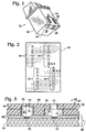
- Fig. 1 is a perspective view of an ink-jet cartridge that carries a print head having an orifice plate formed in accordance with a preferred embodiment of the present invention.
- Fig. 2 is an enlarged plan view of a print head depicting an arrangement of four orifice sets that are associated with four colors of ink carried in the cartridge.
- Fig. 3 is an enlarged cross sectional view of a print head as taken along line 3 - 3 of Fig. 2 and showing an orifice plate made in accordance with a preferred embodiment of the present invention.
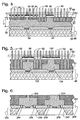
- Figs. 4 - 5 are diagrams showing preferred steps undertaken in making an orifice plate in accord with the present invention.
- Fig. 6 is a cross sectional diagram showing another preferred embodiment of a print head and orifice plate made in accordance with the present invention.
-
- With reference to Fig. 1, a preferred embodiment of the present invention is carried on an ink-
jet cartridge 20. Thecartridge 20 includesplastic body 22 that comprises liquid ink reservoirs for separately containing four supplies of ink: cyan, yellow, magenta, and black ink. - The
pen body 22 is shaped to have a downwardly extendingsnout 24. Aprint head 26 is attached to the underside of thesnout 24. The print head is formed with minute orifices from which are ejected ink droplets onto the printing medium. - As shown in Fig. 2, the orifices are arranged in sets of several individual orifices: a cyan set 30, a
yellow set 32, amagenta set 34, and ablack set 36. Each set has conducted to it the ink color associated with its name. Fig. 2 depicts the outer surface of the print head, which is covered by an orifice plate 40 (Fig. 3) formed in accordance with the present invention, and described more fully below. It is noteworthy here, however, that the term "orifice plate" is hereafter intended to mean a unitary member that combines into one layer the orifices, ink chambers (hence eliminating a separate barrier layer), and, in at least one embodiment, channels of the print head. - Fig. 3 shows a partial cross section of the
print head 26 as taken along line 3 - 3 of Fig. 2, thereby depicting oneorifice 42 of theset 36 of black orifices and oneorifice 44 of theset 34 of magenta orifices. - The print head includes a
substrate 48 that has asilicon base 50, which is preferably a conventional silicon wafer upon which has been grown an insulation layer, such as silicon dioxide. As described in the prior art, such as US Patent No. 4,719,477, the substrate includes a layer of resistive material, such as tantalum aluminum,portions 52 of which are individually connected by conductive layers to traces on a flex circuit 54 (Fig. 1) that is mounted to the exterior of thecartridge 20. Those traces terminate incontacts 56 that mate with like contacts on a printer carriage (not shown), which in turn is connected, as by a ribbon-type multi conductor, to the microprocessor of the printer. - Returning to Fig. 3, the
individual portions 52 of the resistive layer, hereafter referred to asresistors 52, are part of what may be collectively referred to as thecontrol layer 58 of thesubstrate 48, which includes passivation and other sub-layers as described, for example, in US Patent 4,719,477. - The
orifice plate 40 is a unitary member that is fixed to the control layer and includes for each orifice an underlying ink chamber that is continuous with the orifice, thus in fluid communication with the orifice. Fig. 3 depicts a representative "color" chamber 60 (connected to the magenta-ink reservoir), and a representative "black" chamber 62 (connected to the black-ink reservoir). Theresistors 52 are selectively driven (heated) with a pulse of electrical current. The heat from the resistor is sufficient to vaporize some of the ink in selected ones of thechambers orifice - A chamber is refilled after each droplet ejection with ink that flows into the chamber through a channel that connects with the corresponding reservoir of ink. One such "color"
channel 64 is shown in Fig. 3 connected with thecolor chamber 60. Another, "black,"channel 66 is shown connected to theblack chamber 62. As will be described in connection with Fig. 6, the ink chambers may also be filled and refilled via slots extending through thesubstrate 50 andcontrol layer 58, so that channels in the orifice plate are not necessary or provided. - The two
chambers unitary orifice plate 40 wherein one (or more)ink chambers 60 may be deeper than anotherchamber 62 that is part of the same unitary orifice plate. Put another way, one (or more) orifices 42 may be deeper than anotherorifice 44 that is part of the same unitary orifice plate. In this regard, depth is considered as measured in the vertical direction in Fig. 3, from theouter surface 68 of theorifice plate 40 toward thesubstrate 48. - In considering the depth of an orifice, it is useful to consider that structure in terms of an annulus, which can be described as the annular portion of the orifice plate that surrounds the orifice and overlies the associated chamber. As shown in the cross section of Fig. 3, one "color"
annulus 70 is present in the volume of orifice plate material that surrounds thecolor orifice 44 and is between the dashedlines 72 that represent the upward projection of theunderlying chamber 60. Similarly, a "black"annulus 74 is depicted in the volume of orifice plate material surrounding theblack orifice 42 and is between the dashedlines 76 that represent the upward projection of theunderlying chamber 62. - With reference to Fig. 3, the depth of the one
channel 66 may be the same as or greater than the depth of anotherchannel 64 in thesame orifice plate 40. When considering channels, the depth dimension, although measured vertically, is intended to mean the distance that the channel extends above thesubstrate 48. - While the foregoing description concerns orifices and chambers that are generally cylindrical in shape, it is understood that the orifices and connected chambers can be configured in any of a variety of shapes. For instance, even if the orifice were cylindrical, the underlying chamber could be square or rectangular (with rounded corners). As such, the annular or annulus portion discussed above would be somewhat frame shaped. The term annulus, therefore, is not intended to be limited to a particular annular or ring shape.
- It will be appreciated that as between two orifices, chambers, or channels, the length (as measured horizontally in Fig. 3) and width (measured in a direction normal to the plane of Fig. 3) could be varied. The present invention, however, is concerned with the variations in the depth dimensions across a single orifice plate, as discussed above. This depth variability, either alone or in combination with variable length and width dimensions, greatly enhances the number of options available to one charged with the design of a print head. For example, the ratio of the depth of a chamber to the combined depth of the chamber and its associated orifice relates to the volume of an ejected droplet, the length of the tail of the droplet, the chamber refill time, and the time required for refilling the chamber after a droplet is ejected. This description now turns to one preferred method of making a unitary orifice plate that has orifices, chambers and channels of various depths.
- Referring first to Fig. 4, shown there is a segment of a print head that generally matches the segment of Fig. 3, albeit prior to complete processing of the segment of Fig. 4. In a preferred embodiment, the production of
orifice plate 40 begins with a base layer ofphotoresist material 80 that is applied over asubstrate 48 that has been fabricated as described above. (Alternatively, the orifice plate could be fabricated on a mandrel, removed and then bonded to a pre-fabricated substrate.) - In a preferred embodiment, the photoresist material 80 (Fig. 4) comprises a photo-polymerizable epoxy resin known generally in the trade as SU-8. One example is that available from MicroChem Corp. of Newton, MA and sold under the name of SU8-10. It will be, appreciated, however, that the orifice plate could comprise any of a number of negative photoresist materials that become insoluble in developing solutions after exposure to electromagnetic radiation, such as UV radiation in the range of 200 - 500 nanometers.
- The
photoresist layer 80 is spun onto the substrate to a depth "D" of about 20 µm. Once applied, thelayer 80 is exposed to UV radiation through amask 82 that is patterned such that the photoresist layer is divided into at least three different types of regions. One region receives no radiation as a result of radiation-blockingpatterns mask 82. These patterns may comprise a thin layer of, for example, chromium. Oneblocking pattern 84 is shaped to conform in plan view (that is, as viewed in direction parallel to the plane of Fig. 4) with the diameter of the relatively small-diameter color orifice 44. Theother blocking pattern 86 matches, in plan view, the diameter of theblack orifice 42. - Surrounding one
blocking pattern 84 is an attenuatingpattern 88 on themask 82 for attenuating the intensity of the source radiation. This pattern may be, for example, a thin layer of interference filter material or a thin, absorbing film such as silver or a nickel, chromium, and iron alloy known as inconel. As a result, a relatively low-intensity annulus of radiation reaches thesurface 68 of thelayer 80. This low-intensity radiation is depicted as thearrows 90 in Fig. 4. - In the regions away from the blocking
patterns patterns 88 the full, relatively high intensity of the source radiation reaches thesurface 68 of the layer. This high intensity radiation is depicted by thearrows 92 in Fig. 4. - The
photoresist layer 80 undergoes polymeric cross-linking in the regions subjected to the radiation. This cross-linking is depicted as the double hatched areas in Fig. 4. More particularly, the regions subjected to the high intensity radiation undergo cross-linking to a depth "D2" that is relatively deeper than the depth "D1" of cross-linking that occurs in the regions subjected to the relatively lower radiation. - The magnitude of the low intensity radiation is selected so that the depth of cross-linking penetration "D1" of the low-intensity regions matches the design depth of the
annulus 70 surrounding thecolor orifice 44. Similarly, the magnitude of the high intensity radiation is selected so that the depth of cross-linking penetration "D2" of the high-intensity regions matches the design depth of theannulus 74 surrounding theblack orifice 42. - Referring to Fig. 5, the
photoresist layer 80 is next subjected to high intensity radiation that is directed to the layer through amask 96 that is patterned to haveblocking patterns surface 68 of the of the layer and cover the parts of thelayer 80 that correspond to theorifices annuli patterns ink chambers - As shown in Fig. 5, the high-intensity radiation employed in this step is selected to ensure that cross-linking occurs throughout the entire depth "D" in the regions exposed to that radiation, such as the regions between the
ink chambers layer 80 is baked (at, for example, 95° for 30 minutes) and developed in a conventional manner to remove the remaining unexposed portions of the layer, such as shown at 102 and 104. Theseunexposed portions continuous color orifice 44 andchamber 60, and to the continuousblack orifice 42 andchamber 62. The development yields theunitary orifice plate 40 of the present invention, including in the same member the variably shaped orifices and ink chambers. - In instances where a channel such as shown at 64, Fig. 3 is desired, the corresponding part of the
mask 96 over thechannel 64 is patterned with an attenuating filter to permit a medium level of intensity to penetrate the layer 80 (Fig. 5) and generate cross-linking to a depth near, but less than "D" as selected by the print head designer. The remaining unexposed portion is removed simultaneously with theunexposed portions - Fig. 6 depicts an alternative print head design wherein the function of the above described channels is replaced with
feed slots undeveloped regions conduits silicon substrate 250. Theseconduits photoresist layer 280. Thatlayer 280 is otherwise processed in a manner as described above in connection with Figs. 4 and 5. - While the present invention has been described in terms of a preferred embodiment, it will be appreciated by one of ordinary skill that the spirit and scope of the invention is not limited to those embodiments, but extend to the various modifications and equivalents as defined in the appended claims.
Claims (10)
- A method of making an orifice plate (40) for an ink-jet pen (20), comprising the steps of:providing on a substrate (48) a layer (80) of photoresist material having an outer surface (68) and a depth;exposing the photoresist layer to define at least two annular portions (72, 76) that extend from the outer surface into the depth of the layer in a manner such that the depth of one annular portion is greater than the depth of the other annular portion;removing parts of the layer that are surrounded by the annular portions, thereby to define an orifice (44, 42) ; andremoving parts (102, 104) of the layer between the annular portions and the substrate, thereby to define for each annular portion a chamber (60, 62) that is continuous with the orifice of that annular portion.
- The method of claim 1 wherein the exposing step includes the steps of directing electromagnetic radiation (92) to the layer in a manner such that the intensity of the radiation directed to one annular portion is different from the intensity of the radiation directed to the other annular portion.
- The method of claim 2 including the step of providing a mask (82) for reducing the intensity level of at least some of the radiation that is directed to the layer.
- The method of claim 1 wherein the removing steps include:exposing the entire depth of the photoresist layer (80) in regions between the annular portions.
- The step of claim 4 wherein the removing steps also include the step of developing the layer (80) to remove unexposed portions (102, 104) of the layer.
- An orifice plate (40) for an ink-jet print head (26) comprising:a base (80) having an outer surface (68) and first and second chambers (62, 60) formed therein, the base being shaped to define first and second annular portions (76, 72) that each have a depth measured from the outer surface, the first annular portion being continuous with the first chamber and the second annular portion being continuous with the second chamber; and
wherein the depth of the first annular portion is greater than the depth of the second annular portion. - The orifice plate (40) of claim 6 further comprising a first and second channel (64, 66), wherein a first channel is connected to the first chamber (60) and the second channel is connected to the second chamber (62) and wherein the depth of the first channel is different from the depth of the second channel.
- The orifice plate (40) of claim 6 wherein the base (80) is a unitary member.
- The orifice plate (40) of claim 6 wherein the base (80) comprises an exposed, baked, and developed layer of photoresist material.
- The orifice plate (40) of claim 6 attached to a substrate (48) that carries at least two heat transducers (52).
Applications Claiming Priority (2)
| Application Number | Priority Date | Filing Date | Title |
|---|---|---|---|
| US335858 | 1999-06-17 | ||
| US09/335,858 US6303274B1 (en) | 1998-03-02 | 1999-06-17 | Ink chamber and orifice shape variations in an ink-jet orifice plate |
Publications (3)
| Publication Number | Publication Date |
|---|---|
| EP1060892A2 true EP1060892A2 (en) | 2000-12-20 |
| EP1060892A3 EP1060892A3 (en) | 2001-02-07 |
| EP1060892B1 EP1060892B1 (en) | 2005-08-10 |
Family
ID=23313528
Family Applications (1)
| Application Number | Title | Priority Date | Filing Date |
|---|---|---|---|
| EP00304403A Expired - Lifetime EP1060892B1 (en) | 1999-06-17 | 2000-05-24 | Ink chamber and orifice shape variations in an ink-jet orifice plate |
Country Status (8)
| Country | Link |
|---|---|
| US (2) | US6303274B1 (en) |
| EP (1) | EP1060892B1 (en) |
| JP (1) | JP3819217B2 (en) |
| KR (1) | KR100776108B1 (en) |
| CN (1) | CN1161237C (en) |
| DE (1) | DE60021800T2 (en) |
| HK (1) | HK1033115A1 (en) |
| SG (1) | SG91253A1 (en) |
Cited By (2)
| Publication number | Priority date | Publication date | Assignee | Title |
|---|---|---|---|---|
| EP1275505A3 (en) * | 2001-07-11 | 2003-03-05 | Canon Kabushiki Kaisha | Liquid ejection head |
| EP2447082A1 (en) * | 2009-06-23 | 2012-05-02 | Canon Kabushiki Kaisha | Liquid jet recording head |
Families Citing this family (26)
| Publication number | Priority date | Publication date | Assignee | Title |
|---|---|---|---|---|
| KR100514711B1 (en) * | 1997-05-14 | 2005-09-15 | 세이코 엡슨 가부시키가이샤 | Method of forming nozzle for injectors and method of manufacturing ink jet head |
| US6482574B1 (en) * | 2000-04-20 | 2002-11-19 | Hewlett-Packard Co. | Droplet plate architecture in ink-jet printheads |
| TW523468B (en) * | 2001-05-03 | 2003-03-11 | Benq Corp | Image output device for improving image resolution and tone expression |
| KR100396559B1 (en) * | 2001-11-05 | 2003-09-02 | 삼성전자주식회사 | Method for manufacturing monolithic inkjet printhead |
| JP3862625B2 (en) * | 2002-07-10 | 2006-12-27 | キヤノン株式会社 | Method for manufacturing liquid discharge head |
| US6739519B2 (en) * | 2002-07-31 | 2004-05-25 | Hewlett-Packard Development Company, Lp. | Plurality of barrier layers |
| US6916090B2 (en) * | 2003-03-10 | 2005-07-12 | Hewlett-Packard Development Company, L.P. | Integrated fluid ejection device and filter |
| US7309467B2 (en) * | 2003-06-24 | 2007-12-18 | Hewlett-Packard Development Company, L.P. | Fluidic MEMS device |
| US7282324B2 (en) * | 2004-01-05 | 2007-10-16 | Microchem Corp. | Photoresist compositions, hardened forms thereof, hardened patterns thereof and metal patterns formed using them |
| US7429335B2 (en) * | 2004-04-29 | 2008-09-30 | Shen Buswell | Substrate passage formation |
| KR100570822B1 (en) * | 2004-05-11 | 2006-04-12 | 삼성전자주식회사 | method for fabricating ink jet head and ink jet head fabricated thereby |
| CN100503248C (en) * | 2004-06-02 | 2009-06-24 | 佳能株式会社 | Head substrate, recording head, head cartridge, recorder, and method for inputting/outputting information |
| US7364268B2 (en) * | 2005-09-30 | 2008-04-29 | Lexmark International, Inc. | Nozzle members, compositions and methods for micro-fluid ejection heads |
| US7310282B2 (en) * | 2005-12-30 | 2007-12-18 | Lexmark International, Inc. | Distributed programmed memory cell overwrite protection |
| US7600850B2 (en) * | 2006-03-01 | 2009-10-13 | Lexmark International, Inc. | Internal vent channel in ejection head assemblies and methods relating thereto |
| US7909428B2 (en) * | 2006-07-28 | 2011-03-22 | Hewlett-Packard Development Company, L.P. | Fluid ejection devices and methods of fabrication |
| US7918366B2 (en) * | 2006-09-12 | 2011-04-05 | Hewlett-Packard Development Company, L.P. | Multiple drop weight printhead and methods of fabrication and use |
| JP5200397B2 (en) * | 2007-03-20 | 2013-06-05 | ブラザー工業株式会社 | Droplet discharge device |
| JP5213569B2 (en) * | 2007-08-31 | 2013-06-19 | キヤノン株式会社 | Inkjet recording head |
| JP5679665B2 (en) | 2009-02-06 | 2015-03-04 | キヤノン株式会社 | Inkjet recording head |
| JP5578859B2 (en) * | 2010-01-14 | 2014-08-27 | キヤノン株式会社 | Liquid discharge head and method of manufacturing liquid discharge head |
| US9610772B2 (en) * | 2011-03-31 | 2017-04-04 | Hewlett-Packard Development Company, L.P. | Printhead assembly |
| CN106457834B (en) * | 2014-06-23 | 2018-10-19 | 惠普发展公司有限责任合伙企业 | Print head assembly |
| WO2016068947A1 (en) * | 2014-10-30 | 2016-05-06 | Hewlett-Packard Development Company, L.P. | Ink jet printhead |
| EP3362291B1 (en) * | 2015-10-12 | 2023-07-26 | Hewlett-Packard Development Company, L.P. | Printhead |
| US20220323973A1 (en) * | 2021-04-08 | 2022-10-13 | Funai Electric Co., Ltd. | Modified fluid jet plume characteristics |
Citations (1)
| Publication number | Priority date | Publication date | Assignee | Title |
|---|---|---|---|---|
| US4719477A (en) | 1986-01-17 | 1988-01-12 | Hewlett-Packard Company | Integrated thermal ink jet printhead and method of manufacture |
Family Cites Families (16)
| Publication number | Priority date | Publication date | Assignee | Title |
|---|---|---|---|---|
| US4380771A (en) * | 1980-06-27 | 1983-04-19 | Canon Kabushiki Kaisha | Ink jet recording process and an apparatus therefor |
| US4847630A (en) | 1987-12-17 | 1989-07-11 | Hewlett-Packard Company | Integrated thermal ink jet printhead and method of manufacture |
| JP2708769B2 (en) * | 1988-03-24 | 1998-02-04 | 株式会社リコー | Liquid jet recording head |
| JPH0371546U (en) | 1989-11-15 | 1991-07-19 | ||
| ATE158988T1 (en) * | 1990-06-15 | 1997-10-15 | Canon Kk | INK JET RECORDING HEAD AND APPARATUS EQUIPPED WITH SUCH HEAD |
| ATE158754T1 (en) * | 1990-12-19 | 1997-10-15 | Canon Kk | PRODUCTION PROCESS FOR LIQUID OUTFLOW RECORDING HEAD |
| JP2925816B2 (en) * | 1991-10-31 | 1999-07-28 | キヤノン株式会社 | Liquid jet recording head, method of manufacturing the same, and recording apparatus equipped with the head |
| US5167776A (en) | 1991-04-16 | 1992-12-01 | Hewlett-Packard Company | Thermal inkjet printhead orifice plate and method of manufacture |
| JP3334894B2 (en) * | 1991-06-19 | 2002-10-15 | セイコーエプソン株式会社 | Ink jet recording head and method of manufacturing the same |
| JP2932877B2 (en) * | 1992-02-06 | 1999-08-09 | セイコーエプソン株式会社 | Method of manufacturing inkjet head |
| EP0569156B1 (en) | 1992-04-28 | 1998-01-21 | Hewlett-Packard Company | Optimizing print quality and reliability in a CYMK printing system |
| JP3143307B2 (en) * | 1993-02-03 | 2001-03-07 | キヤノン株式会社 | Method of manufacturing ink jet recording head |
| JPH07156409A (en) | 1993-10-04 | 1995-06-20 | Xerox Corp | Ink jet printing head with integrally formed flow path structure and its production |
| JP3441848B2 (en) * | 1995-06-19 | 2003-09-02 | キヤノン株式会社 | Method of manufacturing ink jet recording head |
| JP3674885B2 (en) * | 1996-08-07 | 2005-07-27 | コニカミノルタホールディングス株式会社 | Inkjet recording head |
| JPH11105296A (en) | 1997-10-02 | 1999-04-20 | Brother Ind Ltd | Manufacture of cavity plate and ink jet head |
-
1999
- 1999-06-17 US US09/335,858 patent/US6303274B1/en not_active Expired - Fee Related
-
2000
- 2000-02-03 SG SG200000594A patent/SG91253A1/en unknown
- 2000-05-24 EP EP00304403A patent/EP1060892B1/en not_active Expired - Lifetime
- 2000-05-24 DE DE60021800T patent/DE60021800T2/en not_active Expired - Lifetime
- 2000-06-13 JP JP2000176221A patent/JP3819217B2/en not_active Expired - Fee Related
- 2000-06-14 KR KR1020000032662A patent/KR100776108B1/en not_active IP Right Cessation
- 2000-06-16 CN CNB001186256A patent/CN1161237C/en not_active Expired - Fee Related
-
2001
- 2001-06-01 HK HK01103809A patent/HK1033115A1/en not_active IP Right Cessation
- 2001-08-17 US US09/932,404 patent/US6454393B2/en not_active Expired - Fee Related
Patent Citations (1)
| Publication number | Priority date | Publication date | Assignee | Title |
|---|---|---|---|---|
| US4719477A (en) | 1986-01-17 | 1988-01-12 | Hewlett-Packard Company | Integrated thermal ink jet printhead and method of manufacture |
Cited By (5)
| Publication number | Priority date | Publication date | Assignee | Title |
|---|---|---|---|---|
| EP1275505A3 (en) * | 2001-07-11 | 2003-03-05 | Canon Kabushiki Kaisha | Liquid ejection head |
| US7036909B2 (en) | 2001-07-11 | 2006-05-02 | Canon Kabushiki Kaisha | Liquid ejection head |
| US7384130B2 (en) | 2001-07-11 | 2008-06-10 | Canon Kabushiki Kaisha | Liquid ejection head |
| EP2447082A1 (en) * | 2009-06-23 | 2012-05-02 | Canon Kabushiki Kaisha | Liquid jet recording head |
| EP2447082A4 (en) * | 2009-06-23 | 2014-01-08 | Canon Kk | Liquid jet recording head |
Also Published As
| Publication number | Publication date |
|---|---|
| US20010053501A1 (en) | 2001-12-20 |
| CN1161237C (en) | 2004-08-11 |
| SG91253A1 (en) | 2002-09-17 |
| EP1060892A3 (en) | 2001-02-07 |
| JP3819217B2 (en) | 2006-09-06 |
| US6454393B2 (en) | 2002-09-24 |
| DE60021800T2 (en) | 2006-06-14 |
| HK1033115A1 (en) | 2001-08-17 |
| DE60021800D1 (en) | 2005-09-15 |
| US6303274B1 (en) | 2001-10-16 |
| JP2001010068A (en) | 2001-01-16 |
| EP1060892B1 (en) | 2005-08-10 |
| KR20010007371A (en) | 2001-01-26 |
| KR100776108B1 (en) | 2007-11-15 |
| CN1278485A (en) | 2001-01-03 |
Similar Documents
| Publication | Publication Date | Title |
|---|---|---|
| EP1060892B1 (en) | Ink chamber and orifice shape variations in an ink-jet orifice plate | |
| JP3152259B2 (en) | Roof shooter type thermal inkjet print head | |
| KR100765666B1 (en) | Methods of fabricating fit firing chambers of different drop weights on a single printhead | |
| KR100563356B1 (en) | Direct imaging polymer fluid jet orifice | |
| US6830325B2 (en) | Ink-jet head | |
| KR100224952B1 (en) | Printhead and print cartridge for ink printer, and print method | |
| US7909428B2 (en) | Fluid ejection devices and methods of fabrication | |
| EP0810095B1 (en) | Inkjet print cartridge design to decrease deformation of the printhead when adhesively sealing the printhead to the print cartridge | |
| EP0705706B1 (en) | Ink jet printing system | |
| EP0564072B1 (en) | Efficient conductor routing for inkjet printhead | |
| JPH0645238B2 (en) | Acoustic ink printer | |
| US7070262B2 (en) | Droplet ejecting head | |
| JPH07164627A (en) | Ink jet printing head formed for eliminating ink jet orbit error | |
| CN100369749C (en) | Method of fabricating ink jet head | |
| JP2004042397A (en) | Liquid ejection head and its manufacturing process | |
| JP2004338401A (en) | Ink jet print head | |
| JP2009119725A (en) | Inkjet recording head and method for manufacturing inkjet recording head | |
| JP2012045776A (en) | Method of manufacturing liquid ejection head, liquid ejection head, and liquid ejection apparatus | |
| US20090315950A1 (en) | Liquid ejection head, method for manufacturing liquid ejection head, and method for manufacturing structure | |
| KR19990077695A (en) | Inkjet printhead orifice plate having related orifices |
Legal Events
| Date | Code | Title | Description |
|---|---|---|---|
| PUAI | Public reference made under article 153(3) epc to a published international application that has entered the european phase |
Free format text: ORIGINAL CODE: 0009012 |
|
| AK | Designated contracting states |
Kind code of ref document: A2 Designated state(s): DE FR GB |
|
| AX | Request for extension of the european patent |
Free format text: AL;LT;LV;MK;RO;SI |
|
| PUAL | Search report despatched |
Free format text: ORIGINAL CODE: 0009013 |
|
| AK | Designated contracting states |
Kind code of ref document: A3 Designated state(s): AT BE CH CY DE DK ES FI FR GB GR IE IT LI LU MC NL PT SE |
|
| AX | Request for extension of the european patent |
Free format text: AL;LT;LV;MK;RO;SI |
|
| RAP1 | Party data changed (applicant data changed or rights of an application transferred) |
Owner name: HEWLETT-PACKARD COMPANY, A DELAWARE CORPORATION |
|
| 17P | Request for examination filed |
Effective date: 20010716 |
|
| AKX | Designation fees paid |
Free format text: DE FR GB |
|
| 17Q | First examination report despatched |
Effective date: 20040127 |
|
| GRAP | Despatch of communication of intention to grant a patent |
Free format text: ORIGINAL CODE: EPIDOSNIGR1 |
|
| GRAS | Grant fee paid |
Free format text: ORIGINAL CODE: EPIDOSNIGR3 |
|
| GRAA | (expected) grant |
Free format text: ORIGINAL CODE: 0009210 |
|
| AK | Designated contracting states |
Kind code of ref document: B1 Designated state(s): DE FR GB |
|
| REG | Reference to a national code |
Ref country code: GB Ref legal event code: FG4D |
|
| REF | Corresponds to: |
Ref document number: 60021800 Country of ref document: DE Date of ref document: 20050915 Kind code of ref document: P |
|
| ET | Fr: translation filed | ||
| PLBE | No opposition filed within time limit |
Free format text: ORIGINAL CODE: 0009261 |
|
| STAA | Information on the status of an ep patent application or granted ep patent |
Free format text: STATUS: NO OPPOSITION FILED WITHIN TIME LIMIT |
|
| 26N | No opposition filed |
Effective date: 20060511 |
|
| REG | Reference to a national code |
Ref country code: GB Ref legal event code: 732E Free format text: REGISTERED BETWEEN 20120329 AND 20120404 |
|
| PGFP | Annual fee paid to national office [announced via postgrant information from national office to epo] |
Ref country code: GB Payment date: 20130424 Year of fee payment: 14 Ref country code: DE Payment date: 20130423 Year of fee payment: 14 |
|
| PGFP | Annual fee paid to national office [announced via postgrant information from national office to epo] |
Ref country code: FR Payment date: 20130626 Year of fee payment: 14 |
|
| REG | Reference to a national code |
Ref country code: DE Ref legal event code: R119 Ref document number: 60021800 Country of ref document: DE |
|
| GBPC | Gb: european patent ceased through non-payment of renewal fee |
Effective date: 20140524 |
|
| REG | Reference to a national code |
Ref country code: DE Ref legal event code: R119 Ref document number: 60021800 Country of ref document: DE Effective date: 20141202 |
|
| REG | Reference to a national code |
Ref country code: FR Ref legal event code: ST Effective date: 20150130 |
|
| PG25 | Lapsed in a contracting state [announced via postgrant information from national office to epo] |
Ref country code: DE Free format text: LAPSE BECAUSE OF NON-PAYMENT OF DUE FEES Effective date: 20141202 |
|
| PG25 | Lapsed in a contracting state [announced via postgrant information from national office to epo] |
Ref country code: GB Free format text: LAPSE BECAUSE OF NON-PAYMENT OF DUE FEES Effective date: 20140524 Ref country code: FR Free format text: LAPSE BECAUSE OF NON-PAYMENT OF DUE FEES Effective date: 20140602 |