EP1060836A2 - Wafer tranfer station for a chemical mechanical polisher - Google Patents
Wafer tranfer station for a chemical mechanical polisher Download PDFInfo
- Publication number
- EP1060836A2 EP1060836A2 EP00305118A EP00305118A EP1060836A2 EP 1060836 A2 EP1060836 A2 EP 1060836A2 EP 00305118 A EP00305118 A EP 00305118A EP 00305118 A EP00305118 A EP 00305118A EP 1060836 A2 EP1060836 A2 EP 1060836A2
- Authority
- EP
- European Patent Office
- Prior art keywords
- wafer
- transfer robot
- load
- workpiece
- gripper
- Prior art date
- Legal status (The legal status is an assumption and is not a legal conclusion. Google has not performed a legal analysis and makes no representation as to the accuracy of the status listed.)
- Withdrawn
Links
Images



Classifications
-
- B—PERFORMING OPERATIONS; TRANSPORTING
- B24—GRINDING; POLISHING
- B24B—MACHINES, DEVICES, OR PROCESSES FOR GRINDING OR POLISHING; DRESSING OR CONDITIONING OF ABRADING SURFACES; FEEDING OF GRINDING, POLISHING, OR LAPPING AGENTS
- B24B41/00—Component parts such as frames, beds, carriages, headstocks
- B24B41/005—Feeding or manipulating devices specially adapted to grinding machines
-
- H—ELECTRICITY
- H10—SEMICONDUCTOR DEVICES; ELECTRIC SOLID-STATE DEVICES NOT OTHERWISE PROVIDED FOR
- H10P—GENERIC PROCESSES OR APPARATUS FOR THE MANUFACTURE OR TREATMENT OF DEVICES COVERED BY CLASS H10
- H10P52/00—Grinding, lapping or polishing of wafers, substrates or parts of devices
-
- B—PERFORMING OPERATIONS; TRANSPORTING
- B24—GRINDING; POLISHING
- B24B—MACHINES, DEVICES, OR PROCESSES FOR GRINDING OR POLISHING; DRESSING OR CONDITIONING OF ABRADING SURFACES; FEEDING OF GRINDING, POLISHING, OR LAPPING AGENTS
- B24B37/00—Lapping machines or devices; Accessories
- B24B37/34—Accessories
- B24B37/345—Feeding, loading or unloading work specially adapted to lapping
-
- H—ELECTRICITY
- H10—SEMICONDUCTOR DEVICES; ELECTRIC SOLID-STATE DEVICES NOT OTHERWISE PROVIDED FOR
- H10P—GENERIC PROCESSES OR APPARATUS FOR THE MANUFACTURE OR TREATMENT OF DEVICES COVERED BY CLASS H10
- H10P72/00—Handling or holding of wafers, substrates or devices during manufacture or treatment thereof
- H10P72/30—Handling or holding of wafers, substrates or devices during manufacture or treatment thereof for conveying, e.g. between different workstations
- H10P72/33—Handling or holding of wafers, substrates or devices during manufacture or treatment thereof for conveying, e.g. between different workstations into and out of processing chamber
- H10P72/3304—Handling or holding of wafers, substrates or devices during manufacture or treatment thereof for conveying, e.g. between different workstations into and out of processing chamber characterised by movements or sequence of movements of transfer devices
-
- Y—GENERAL TAGGING OF NEW TECHNOLOGICAL DEVELOPMENTS; GENERAL TAGGING OF CROSS-SECTIONAL TECHNOLOGIES SPANNING OVER SEVERAL SECTIONS OF THE IPC; TECHNICAL SUBJECTS COVERED BY FORMER USPC CROSS-REFERENCE ART COLLECTIONS [XRACs] AND DIGESTS
- Y10—TECHNICAL SUBJECTS COVERED BY FORMER USPC
- Y10S—TECHNICAL SUBJECTS COVERED BY FORMER USPC CROSS-REFERENCE ART COLLECTIONS [XRACs] AND DIGESTS
- Y10S414/00—Material or article handling
- Y10S414/135—Associated with semiconductor wafer handling
Definitions
- the present invention relates generally to a chemical mechanical polishing system. More specifically, the invention relates a method and apparatus for positioning a workpiece or semiconductor wafer into a chemical mechanical polishing system.
- CMP chemical mechanical polishing
- the wafer is released from the robot and secured, or chucked, to the pedestal by a vacuum chuck.
- the pedestal is then retracted into the transfer station wherein the wafer is temporarily released from the pedestal so that a plurality of alignment jaws may manipulate the wafer into a position centered upon the pedestal.
- the wafer is then rechucked to the pedestal and the pedestal rises to engage and transfer the wafer to a retaining ring of a polishing head.
- the alignment of the wafer to the center of the pedestal ensures that the wafer will be properly fixtured into the retaining ring.
- a carousel moves the polishing head to a polishing station.
- the wafer is returned to the pedestal where a robot retrieves the wafer and moves it to the proper cassette located in the bath.
- a single arm robot with a single end effector for gripping a wafer obtains a wafer from a wafer storage device, positions the wafer upon a single load/ unload pedestal. The wafer enters the polisher and work is polished. The wafer is then returned to the load/unload pedestal for unloading and transporting to a wafer storage device.
- the single arm robot must then grip the processed wafer and transport it to a wafer storage device, place the wafer in the device, and index down and retrieve the next wafer to be processed in the polisher.
- the robot then transports the next wafer to the load/unload pedestal for drop off. Elimination of the dwell time or the dead time in which the load/unload pedestal is idle would improve the routing time required to process each wafer, and yield a corresponding increase in wafer throughput.
- the use of wafer edge grip only would minimize physical contact with either the backside surface or the device surface of the wafer during transporting and wafer placement. This is of special concern since any abrasion, scratching or other damage could occur on either side of the wafer.
- a transfer station comprising at least one buffer station, a transfer robot, and a wafer loading assembly.
- a plurality of buffer stations is used, e.g., an input buffer station and an output buffer station.
- an input/output robot places a semiconductor wafer into an input buffer station.
- the input buffer station supports the wafer on three pins proximate the edge of the wafer.
- the transfer robot has two gripper assemblies, each having pneumatic gripper fingers that grab the wafer. The fingers retain the wafer at three points on the edge of the wafer.
- the robot lifts the wafer from the input buffer station and rotates the gripper and wafer to position the wafer over the wafer load/unload assembly, then places the wafer down onto the 5 load/unload assembly.
- the wafer load/unload assembly then loads the wafer into a polishing head of the chemical mechanical polisher. While the transfer robot is positioning the wafer into the wafer load/unload assembly, the input/output robot may be positioning another wafer upon the input buffer station. Once a wafer has completed the polishing process, the polishing head releases the wafer into the wafer load/unload assembly, and the transfer robot removes the wafer from the load/unload assembly.
- the polished wafer is then placed in the output buffer station by the transfer robot where it remains until the input/output robot removes the polished wafer from the transfer station.
- the transfer robot has two gripper assemblies, the steps of releasing the wafer into the load/unload assembly and the output buffer can occur simultaneously.
- the transfer robot comprises a pair of opposing gripper assemblies that are pneumatically actuated.
- Each of the gripper assemblies is located on opposing distal ends of two transfer arms.
- the transfer arms are coupled to a rotary actuator and a vertical linear actuator such that the grippers can be rotated from the buffer stations to the load/unload assembly and the robot arms can be raised and lowered to facilitate loading and unloading wafers.
- the grippers themselves have three fingers, plastic cylinders with a notch cut into the cylinder, to grip the edge of the wafer therein.
- the grippers are biased in an open position by springs such that the distance between the fingers of each gripper is greater than the diameter of a wafer. When compressed air is forced into a pneumatic cylinder, the grippers move towards one another and a wafer is captured between the three fingers.
- Each of the transfer arms has a gripper assembly located at a first end and terminates in a second end that is mounted to a vertical shaft.
- the shaft is coupled to a rotary actuator through a clutch such that the arm can be rotated about 350 degrees.
- the shaft is coupled to an interlock mechanism that ensures that the transfer robot is properly position over either a buffer station or the wafer load/unload assembly before the transfer robot is allowed to be lowered into the buffer stations or the loadcup to release or pick-up a wafer.
- the interlock also ensures that the transfer robot cannot rotate toward the wafer load/unload assembly when that assembly is loading (or unloading) a wafer into the polishing head.
- the buffer station and the wafer load/unload assembly are aligned along a circular path having the shaft of the transfer robot at its center.
- FIG. 1 depicts a schematic top plan view of a chemical mechanical polisher 100.
- the polisher 100 has a plurality of polishing stations 106 (e.g., three), a carousel 102 that supports four polishing heads 110, a wafer load/unload assembly 104, and a transfer station 108.
- An input/output robot 116 loads and unloads wafers 114 to/from the transfer station 108.
- Four polishing heads 110 are mounted in the carousel 102.
- the carousel 102 is partially cut-away to provide a view of the components of the transfer station 108. As such, one of the four polishing heads 110 is not shown.
- the carousel 102 rotates about a central axis such that any one of the polishing heads 110 may be positioned at any one of the polishing stations 106 or the transfer station 108. Consequently, the wafer 114 can be loaded into a particular polishing head 110, and the carousel 102 can move the head 110 to a particular polishing station 106.
- the wafer 114 is transferred between the polisher 100 and other systems (e.g., wafer cleaners) or wafer cassettes (not shown) via the wafer input/output robot 116.
- the input/output robot 116 has a gripper 118 (e.g., a vacuum gripper) that retains the wafer 114 during transfer, and sets the wafer 114 into the transfer station 108.
- the transfer station 108 comprises at least one buffer station 120 (preferably, two buffer stations 120A and 120B) and a transfer robot 122.
- the input/output robot 116 places the wafer 114 that is entering the polisher 100 into the input buffer station 120B.
- the input buffer station 120B is stationary.
- the transfer station robot 122 retrieves the wafer 114 from the input buffer station 120B and moves the wafer 114 to the wafer load/unload assembly 104.
- the wafer load/unload assembly 104 may be of any type known in the art for positioning the wafer 114 into a polishing head 110.
- the wafer load/unload assembly 104 is a load cup that is described in commonly assigned U.S. provisional patent application 60/139,144, filed June 14, 1999, (Attorney Docket Number 3650L) and incorporated herein by reference.
- the carousel 102 retrieves the wafer 114 from the wafer load/unload assembly 104 and proceeds to polish the wafer 114. While the transfer robot 122 is busy moving a wafer 114 from the buffer station 120 to the wafer load/unload assembly 104, the input/output robot 116 may position another wafer 114 into the empty input buffer station 120B.
- the carousel 102 moves the wafer 114 to the wafer load/unload assembly 104 and releases the wafer 114.
- the transfer robot 122 then retrieves the wafer 114 from the wafer load/unload assembly 104 and places the wafer 114 into the output buffer station 120A.
- the polished wafer 114 is then retrieved from the output buffer station 120B by the input/output robot 116.
- the transfer robot 122 is centrally located between the buffer stations 120A, 120B and the wafer load/unload assembly 104.
- the robot 122 has a central axis of rotation that is concentric with an imaginary circle that passes through the center of buffer stations 120A, 120B and the wafer load/unload assembly 104 such that the transfer robot 122 reaches these locations without using an articulating arm.
- the transfer robot 122 may readily substitute other variations of robots while maintaining the ability to position the wafer 114 in the buffer stations 120A, 120B and the wafer load/unload assembly 104.
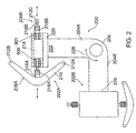
- FIG. 2 depicts a top plan view of an arm assembly 200 of the transfer robot (122 of FIG. 1).
- the arm assembly 200 comprises a pair of identical gripper assemblies 202A and 202B, a pair of transfer arms 204A and 204B, and an arm mounting location 206.
- the gripper assembly 202A (gripper assembly 202B is identically composed) comprises a pair of opposing grippers 208A and 208B.
- the gripper 208A comprises a gripper arm 210 and a pair of fingers 212A, 212B.
- the gripper arm 210 has a chevron shape with the point of the chevron facing outwards.
- the gripper 208B has a single finger 212C.
- Each of the fingers 212A, 212B are downwardly pointing and are located proximate the distal ends of the gripper arm 210.
- Finger 212C is downwardly pointing and lies in a plane with the other two fingers 212A and 212B.
- the center portion of the gripper arm 210 is coupled to a linear actuator 214.
- the actuator 214 has a pair of actuator shafts 216A and 216B that protrude in opposite directions from the actuator 114.
- the shaft 216A couples the actuator 214 to the gripper arm 210 and the shaft 216B couples the actuator 214 to the finger 212C that forms gripper 208B.
- the shafts 216A and 216B as well as the actuator 214 are protected from particulate contamination by a pair of bellows 218A and 218B surrounding each shaft and abutting an actuator housing 220.
- the gripper assemblies 202A and 202B permit the transfer robot 112 to simultaneously hold wafers in each assembly. This allows the transfer robot 112 to place the polished wafer into the output buffer station 120A while simultaneously placing the unpolished wafer into the load/unload assembly 104.
- the actuator 214 is a linear actuator that moves the shafts 216A and 216B inward and outward from the housing 220. Shafts 216A and 216B are supported on linear bearings 900 and 901 to minimize side loads into the linear actuator.
- One example of an actuator 214 is a pneumatic actuator that moves the shafts in response to air pressure. Such an actuator 214 has the shafts 216A and 216B biased outwardly by springs (not shown) that maintain the grippers 208A and 208B apart from one another in an open position. In the open position, the spacing between the fingers is larger than the diameter the wafer (e.g., 100, mm, 200 mm, or 300 mm).
- the actuator 214 moves the shafts 216 inwardly to cause the fingers 212A, 212B, and 212C to grip and retain a wafer (not shown in FIG. 2).
- Force applied to the fingers 212A, 212B and 212C, and hence the wafer 114, is proportional to the air pressure applied to the pneumatic actuator and can be regulated to minimize the force, thus substantially preventing wafer- damage and contamination.
- Alternative linear actuators include, but are not limited to, worm gear assemblies, solenoids, rack and pinion assemblies, bell cranks, and the like. Additionally, more fingers and/or fingers of various shapes and sizes could be provided to facilitate wafer gripping.
- FIG. 3 depicts side view of the gripper arm 210, and its associated fingers 212A and 212B that are bolted proximate the ends 302 of the arm 210.
- Each finger has a cylindrical shape containing a notch 304 cut into a side of the cylinder. These notches 304 have an opening that is larger than the thickness of a wafer.
- the fingers are fabricated of a non-abrasive material such as plastic.
- the actuator housing 220 is attached to a distal end 222 (a first end) of the arm 204A.
- the arm 204A is connected to the arm 204B having a second gripper assembly 202B coupled to the distal end 226 thereof.
- the arms 204B and 204A at an angle to each other, preferably forming a right angle with respect to one another.
- the arms are attached to the robot's rotary and vertical actuators (not shown).
- the robot is coupled to a rotary actuator that rotates the arm as indicated by arrow 228.
- FIG. 4 depicts a side plan view of the transfer station 108 comprising the transfer robot 122 carrying a wafer 400 and one of the buffer stations, e.g., station 120A, in partial cross section. For completeness, also depicted is the wafer load/unload assembly 104.
- the transfer robot 122, the wafer load/unload assembly 104 and the buffer stations 120A, 120B are mounted to a common base plate 418 for the transfer station 108.
- the arm 204A of the transfer robot 122 couples the gripper assembly 202A to the mounting point 206.
- the mounting point 206 is affixed to a tube shaft 402.
- the tube shaft 402 and a spindle 406 are coaxially assembled and mechanically form a slip clutch 404.
- a rotary actuator 408 rotationally drives the spindle 406.
- the slip clutch 404 ensures that the rotary actuator 408 and spindle 406 are able to rotate without being damaged if the robot arm 204 were to malfunction and become unable to move, i.e., become stuck.
- the clutch 404 and tube shaft 402 pass concentrically through protective cylinders 410 and 411.
- the protective cylinders 410 and 411 are fastened to the base plate 418.
- the shield 416 and protective cylinders 410 and 411 form a labyrinth seal 401 that impedes the slurry from the polishing process from interfering with the operation of the clutch 404 and other lower mechanisms.
- the transfer robot 122 further comprises a cam plate 420 that is affixed to and rotates with the tube shaft 402.
- the cam plate 420 interacts with an interlock assembly 422 and a pin 423.
- the interlock assembly 422 ensures that the transfer robot 122 can not rotate towards the wafer load/unload assembly 104 and make contact when the loading/unloading assembly 104 is loading a wafer 400 into the polishing head.
- the load/unload assembly 104 comprises a vertical actuator 450 that drives a shaft 452 for lifting the wafer 400 into the polishing head.
- the shaft 452 has a linear cam 454 that abuts the interlock cam 422. When the load/unload assembly 104 rises, causing the interlock cam 454 to rotate outward on pivot 456.
- the cam plate 420 is an irregular shape that allows the transfer robot 122 to rotate freely between the buffer stations. However, when the transfer robot 122 rotates toward the load/unload assembly 104, the cam plate 420 abuts the interlock assembly 422 and rotation is halted. When rotation is halted, the clutch 404 will slip, ensuring that the transfer robot 122 does not impact the load/unload assembly 104.
- the transfer robot 122 operates in three vertical positions.
- the down position is a position that is used to retrieve or place wafers onto the load/unload assembly 104 or either of the buffer stations 120A or 120B.
- the pin 423 interacts with holes and slots in the cam plate 420 to ensure that the transfer robot 122 does not rotate when the transfer robot 122 is in a down position, and that the transfer robot 122 lowers in the angular position to the load/unload assembly 104 and buffer stations 120A and 120B.
- the transfer robot 122 cannot rotate.
- the cam plate 420 does not interact with the pin 423 and the transfer robot 122 may freely rotate about 350 degrees, unless the wafer load/unload assembly 104 is loading a wafer 400 into a polishing head 110.
- the transfer robot 122 can rotate proximate the buffer stations.
- flange 458 will abut the cam plate 420 if the transfer robot 122 attempts to rotate toward the wafer load/unload assembly 104. This ensures that the transfer robot 122 cannot impact the polishing head 110 while rotating in the up position.
- the buffer station 120 comprises a wafer support 426 that is supported by a plurality of bolts 428 above the base plate 418.
- the bores 432 in the wafer support 426 are much larger than the bolt 428 diameter such that the wafer support 426 can move laterally with respect to the base plate 418.
- This feature allows the buffer station to be aligned with the radial and angular position of the transfer robot 122 at the drop-off or pick-up location specified by the transfer robot position during setup.
- the buffer station With a wafer 400 in the transfer robot grippers and at the desired position for wafer transfer, the buffer station is located beneath the supported wafer and the transfer robot 122 lowers the wafer 400 down to the set vertical distance fixed by an adjustment screw on the transfer robot 122.
- the wafer support 426 is aligned vertically and laterally to be concentric to the held wafer.
- the wafer support is affixed to the base plate by fasteners.
- FIG. 5 depicts a top plan view of the wafer support 426.
- the wafer support 426 is circular in plan form and comprises a circumferential lip 500, three cut outs 502A, 502B and 502C, mounting bolts 428, and wafer support pins 506A, 506B, and 506C.
- the circumferential lip 500 rises above the plane of a central portion 508 of the wafer support 426 such that a wafer will not slide off of the support when resting on the three wafer support pins.
- the cut outs 502A, 502B, and 502C are provided to enable the gripper fingers to access a wafer.
- a wafer rests above the plane of the central portion 508 upon pins 506A, 506B and 506C.
- the pins could be solid; however, to facilitate wafer detection, the pins are hollow.
- a fluid water
- the flow of water is monitored to detect flow change when a wafer is present.
- Such a change in flow is used to indicate when a wafer is positioned on a buffer station.
- the small fluid (water) film between the wafer and the support pins ensures that the wafer does not contact the pin and thereby minimizes particle contamination to the wafer surfaces.
Landscapes
- Engineering & Computer Science (AREA)
- Mechanical Engineering (AREA)
- Mechanical Treatment Of Semiconductor (AREA)
- Container, Conveyance, Adherence, Positioning, Of Wafer (AREA)
- Finish Polishing, Edge Sharpening, And Grinding By Specific Grinding Devices (AREA)
- Manipulator (AREA)
Abstract
Description
Claims (20)
- Apparatus for positioning a workpiece comprising:at least one buffer station;a transfer robot; anda load/unload assembly, wherein said transfer robot positions said workpiece selectively on said buffer station and said load/unload assembly.
- An apparatus as claimed in claim 1, wherein said at least one buffer station comprises a loading station; and an unloading station.
- An apparatus as claimed in claim 1, wherein said transfer robot further comprises a first transfer arm having a first gripper and a second transfer arm disposed at an angle to said first transfer arm, said second transfer arm having a second gripper.
- An apparatus as claimed in claim 3, wherein said first gripper and said second gripper each comprise a plurality of gripper fingers.
- An apparatus as claimed in any of claims 1 to 4, wherein said transfer robot further comprises a rotatable tube shaft comprising slip clutch.
- An apparatus as claimed in claim 5, wherein said transfer robot further comprises a shield circumscribing said tube shaft and a first cylinder and a second cylinder concentrically disposed about said tube shaft, said shield, said first cylinder and said second cylinder defining a labyrinth seal.
- An apparatus as claimed in claim 5 or claim 6, wherein said transfer robot further comprises a cam plate affixed to said tube shaft.
- An apparatus as claimed in claim 7, wherein said transfer robot further comprises an interlock assembly and a pin, said interlock assembly and said pin selectively engaging said cam plate in a position preventing rotation of said transfer robot.
- An apparatus as claimed in any of claims 1 to 8, and further comprising a base plate connected to said at least one buffer station, said transfer robot and said load/unload assembly.
- An apparatus as claimed in any of claims 1 to 9, wherein said load/unload assembly comprises a linear actuator.
- An apparatus as claimed in any of claims 1 to 10, and further comprising a chemical mechanical polisher.
- Apparatus for positioning a workpiece comprising:a buffer station having an input and an output buffer;a transfer robot having a first and a second gripper; anda load/unload assembly, wherein said transfer robot positions said workpiece selectively on said buffer station and said load/unload assembly.
- An apparatus as claimed in claim 12, wherein said load/unload assembly is disposed within a chemical mechanical polisher.
- An apparatus as claimed in claim 13, wherein said first and said second gripper each further comprises a plurality of gripper fingers, each of said gripper fingers having a notch, said notch selectively securing said workpiece by an edge.
- A chemical mechanical polisher comprising:a plurality of polishing stations, at least one buffer station,a transfer robot, anda load/unload assembly, wherein said transfer robot positions said workpiece selectively on said buffer station and said load/unload assembly.
- A chemical mechanical polisher as claimed in claim 15, wherein said transfer robot further comprises:a rotatable tube shaft;a first and a second gripper coupled to said tube shaft;a slip clutch disposed within said tube shaft;a cam plate affixed to said tube shaft;a shield circumscribing said tube shaft;a first cylinder and a second cylinder concentrically disposed about said tube shaft, said shield, said first cylinder and said second cylinder defining a labyrinth seal; andan interlock assembly and a pin, said interlock assembly and said pin selectively engaging said cam plate in a position preventing rotation.
- A method for positioning a workpiece comprising the steps of:retrieving an first workpiece in a first gripper of a transfer robot;retrieving a second workpiece in a second gripper of the transfer robot;placing the first workpiece in a load/unload assembly; andplacing the second workpiece in an output buffer station.
- A method according to claim 17, wherein the step of retrieving the first wafer further comprise the steps of:actuating the transfer robot into a lower position; andpreventing the transfer robot from rotating.
- A method according to claim 17, wherein the steps of placing the first workpiece in the load/unload assembly and placing the second workpiece in the output buffer station occur simultaneously.
- A method as claimed in claim 17, wherein the first workpiece is an unpolished wafer and the second workpiece is a polished wafer.
Applications Claiming Priority (4)
| Application Number | Priority Date | Filing Date | Title |
|---|---|---|---|
| US13984699P | 1999-06-18 | 1999-06-18 | |
| US139846P | 1999-06-18 | ||
| US09/414,771 US6156124A (en) | 1999-06-18 | 1999-10-06 | Wafer transfer station for a chemical mechanical polisher |
| US414771 | 1999-10-06 |
Publications (2)
| Publication Number | Publication Date |
|---|---|
| EP1060836A2 true EP1060836A2 (en) | 2000-12-20 |
| EP1060836A3 EP1060836A3 (en) | 2003-03-26 |
Family
ID=26837596
Family Applications (1)
| Application Number | Title | Priority Date | Filing Date |
|---|---|---|---|
| EP00305118A Withdrawn EP1060836A3 (en) | 1999-06-18 | 2000-06-16 | Wafer tranfer station for a chemical mechanical polisher |
Country Status (4)
| Country | Link |
|---|---|
| US (2) | US6156124A (en) |
| EP (1) | EP1060836A3 (en) |
| JP (2) | JP2001060571A (en) |
| KR (1) | KR20010049569A (en) |
Cited By (3)
| Publication number | Priority date | Publication date | Assignee | Title |
|---|---|---|---|---|
| WO2003092068A1 (en) * | 2002-04-24 | 2003-11-06 | Tokyo Electron Limited | Substrate conveying mechanism and substrate conveying method |
| US6854948B1 (en) | 2002-08-15 | 2005-02-15 | Nanometrics Incorporated | Stage with two substrate buffer station |
| CN109531629A (en) * | 2018-11-15 | 2019-03-29 | 厦门朴蜂智能科技有限公司 | High-altitude outer wall operation robot negative-pressure adsorption safety device |
Families Citing this family (88)
| Publication number | Priority date | Publication date | Assignee | Title |
|---|---|---|---|---|
| US6358128B1 (en) | 1999-03-05 | 2002-03-19 | Ebara Corporation | Polishing apparatus |
| US6354922B1 (en) | 1999-08-20 | 2002-03-12 | Ebara Corporation | Polishing apparatus |
| KR20010020807A (en) | 1999-05-03 | 2001-03-15 | 조셉 제이. 스위니 | Pre-conditioning fixed abrasive articles |
| US6156124A (en) * | 1999-06-18 | 2000-12-05 | Applied Materials, Inc. | Wafer transfer station for a chemical mechanical polisher |
| US6679755B1 (en) | 1999-12-09 | 2004-01-20 | Applied Materials Inc. | Chemical mechanical planarization system |
| US7303462B2 (en) | 2000-02-17 | 2007-12-04 | Applied Materials, Inc. | Edge bead removal by an electro polishing process |
| US6991526B2 (en) | 2002-09-16 | 2006-01-31 | Applied Materials, Inc. | Control of removal profile in electrochemically assisted CMP |
| US6848970B2 (en) | 2002-09-16 | 2005-02-01 | Applied Materials, Inc. | Process control in electrochemically assisted planarization |
| US7125477B2 (en) | 2000-02-17 | 2006-10-24 | Applied Materials, Inc. | Contacts for electrochemical processing |
| US6991528B2 (en) | 2000-02-17 | 2006-01-31 | Applied Materials, Inc. | Conductive polishing article for electrochemical mechanical polishing |
| US7059948B2 (en) | 2000-12-22 | 2006-06-13 | Applied Materials | Articles for polishing semiconductor substrates |
| US7066800B2 (en) | 2000-02-17 | 2006-06-27 | Applied Materials Inc. | Conductive polishing article for electrochemical mechanical polishing |
| US20030213703A1 (en) * | 2002-05-16 | 2003-11-20 | Applied Materials, Inc. | Method and apparatus for substrate polishing |
| US7029365B2 (en) | 2000-02-17 | 2006-04-18 | Applied Materials Inc. | Pad assembly for electrochemical mechanical processing |
| US7303662B2 (en) | 2000-02-17 | 2007-12-04 | Applied Materials, Inc. | Contacts for electrochemical processing |
| US7678245B2 (en) | 2000-02-17 | 2010-03-16 | Applied Materials, Inc. | Method and apparatus for electrochemical mechanical processing |
| US6979248B2 (en) | 2002-05-07 | 2005-12-27 | Applied Materials, Inc. | Conductive polishing article for electrochemical mechanical polishing |
| US7077721B2 (en) | 2000-02-17 | 2006-07-18 | Applied Materials, Inc. | Pad assembly for electrochemical mechanical processing |
| US6962524B2 (en) | 2000-02-17 | 2005-11-08 | Applied Materials, Inc. | Conductive polishing article for electrochemical mechanical polishing |
| US7374644B2 (en) | 2000-02-17 | 2008-05-20 | Applied Materials, Inc. | Conductive polishing article for electrochemical mechanical polishing |
| US7670468B2 (en) | 2000-02-17 | 2010-03-02 | Applied Materials, Inc. | Contact assembly and method for electrochemical mechanical processing |
| US6896776B2 (en) | 2000-12-18 | 2005-05-24 | Applied Materials Inc. | Method and apparatus for electro-chemical processing |
| US6406362B1 (en) * | 2001-01-04 | 2002-06-18 | Speedfam-Ipec Corporation | Seal for use with a chemical mechanical planarization apparatus |
| US6942545B2 (en) * | 2001-04-20 | 2005-09-13 | Oriol, Inc. | Apparatus and method for sequentially polishing and loading/unloading semiconductor wafers |
| US7344432B2 (en) | 2001-04-24 | 2008-03-18 | Applied Materials, Inc. | Conductive pad with ion exchange membrane for electrochemical mechanical polishing |
| US7137879B2 (en) | 2001-04-24 | 2006-11-21 | Applied Materials, Inc. | Conductive polishing article for electrochemical mechanical polishing |
| US6503131B1 (en) | 2001-08-16 | 2003-01-07 | Applied Materials, Inc. | Integrated platen assembly for a chemical mechanical planarization system |
| US6837983B2 (en) * | 2002-01-22 | 2005-01-04 | Applied Materials, Inc. | Endpoint detection for electro chemical mechanical polishing and electropolishing processes |
| US6841057B2 (en) | 2002-03-13 | 2005-01-11 | Applied Materials Inc. | Method and apparatus for substrate polishing |
| US6739958B2 (en) | 2002-03-19 | 2004-05-25 | Applied Materials Inc. | Carrier head with a vibration reduction feature for a chemical mechanical polishing system |
| JP4254116B2 (en) * | 2002-03-22 | 2009-04-15 | 東京エレクトロン株式会社 | Substrate for alignment |
| US20050061674A1 (en) | 2002-09-16 | 2005-03-24 | Yan Wang | Endpoint compensation in electroprocessing |
| US7112270B2 (en) | 2002-09-16 | 2006-09-26 | Applied Materials, Inc. | Algorithm for real-time process control of electro-polishing |
| US7842169B2 (en) * | 2003-03-04 | 2010-11-30 | Applied Materials, Inc. | Method and apparatus for local polishing control |
| KR100512179B1 (en) * | 2003-06-19 | 2005-09-02 | 삼성전자주식회사 | chemical and mechanical polishing apparatus for manufacturing a semiconductor |
| US20050171551A1 (en) * | 2003-10-21 | 2005-08-04 | William Sukovich | Instrument and method for preparing a bone to receive an implant |
| JP2005167208A (en) * | 2003-10-24 | 2005-06-23 | Ade Corp | Notch / flat 200mm wafer edge grip end effector |
| US7186164B2 (en) | 2003-12-03 | 2007-03-06 | Applied Materials, Inc. | Processing pad assembly with zone control |
| DE102005000645B4 (en) | 2004-01-12 | 2010-08-05 | Samsung Electronics Co., Ltd., Suwon | Apparatus and method for treating substrates |
| US7390744B2 (en) | 2004-01-29 | 2008-06-24 | Applied Materials, Inc. | Method and composition for polishing a substrate |
| US7084064B2 (en) | 2004-09-14 | 2006-08-01 | Applied Materials, Inc. | Full sequence metal and barrier layer electrochemical mechanical processing |
| US7520968B2 (en) | 2004-10-05 | 2009-04-21 | Applied Materials, Inc. | Conductive pad design modification for better wafer-pad contact |
| US7655565B2 (en) | 2005-01-26 | 2010-02-02 | Applied Materials, Inc. | Electroprocessing profile control |
| US7427340B2 (en) | 2005-04-08 | 2008-09-23 | Applied Materials, Inc. | Conductive pad |
| KR20070112397A (en) * | 2005-05-12 | 2007-11-23 | 어플라이드 머티어리얼스, 인코포레이티드 | Method and apparatus for vertical transfer of semiconductor substrate into cleaning module |
| US8617672B2 (en) | 2005-07-13 | 2013-12-31 | Applied Materials, Inc. | Localized surface annealing of components for substrate processing chambers |
| US20070153453A1 (en) * | 2006-01-05 | 2007-07-05 | Applied Materials, Inc. | Fully conductive pad for electrochemical mechanical processing |
| US20090067959A1 (en) * | 2006-02-22 | 2009-03-12 | Nobuyuki Takahashi | Substrate processing apparatus, substrate transfer apparatus, substrate clamp apparatus, and chemical liquid treatment apparatus |
| JP2007242648A (en) * | 2006-03-04 | 2007-09-20 | Masato Toshima | Substrate processing equipment |
| US20070235344A1 (en) * | 2006-04-06 | 2007-10-11 | Applied Materials, Inc. | Process for high copper removal rate with good planarization and surface finish |
| EP2005808B1 (en) * | 2006-04-12 | 2010-03-17 | Kulicke & Soffa Die Bonding GmbH | Method and device for placing electronic components, especially semiconductor chips, on a substrate |
| US20070251832A1 (en) * | 2006-04-27 | 2007-11-01 | Applied Materials, Inc. | Method and apparatus for electrochemical mechanical polishing of cu with higher liner velocity for better surface finish and higher removal rate during clearance |
| US7166016B1 (en) | 2006-05-18 | 2007-01-23 | Applied Materials, Inc. | Six headed carousel |
| WO2007143566A2 (en) * | 2006-06-02 | 2007-12-13 | Applied Materials, Inc. | Fast substrate loading on polishing head without membrane inflation step |
| US20070281589A1 (en) * | 2006-06-02 | 2007-12-06 | Applied Materials, Inc. | Rotational alignment mechanism for load cups |
| US7422982B2 (en) | 2006-07-07 | 2008-09-09 | Applied Materials, Inc. | Method and apparatus for electroprocessing a substrate with edge profile control |
| US20080014845A1 (en) * | 2006-07-11 | 2008-01-17 | Alpay Yilmaz | Conditioning disk having uniform structures |
| US7651384B2 (en) * | 2007-01-09 | 2010-01-26 | Applied Materials, Inc. | Method and system for point of use recycling of ECMP fluids |
| US7981262B2 (en) | 2007-01-29 | 2011-07-19 | Applied Materials, Inc. | Process kit for substrate processing chamber |
| US8012000B2 (en) * | 2007-04-02 | 2011-09-06 | Applied Materials, Inc. | Extended pad life for ECMP and barrier removal |
| US7942969B2 (en) | 2007-05-30 | 2011-05-17 | Applied Materials, Inc. | Substrate cleaning chamber and components |
| US8523639B2 (en) * | 2008-10-31 | 2013-09-03 | Applied Materials, Inc. | Self cleaning and adjustable slurry delivery arm |
| TWI417984B (en) | 2009-12-10 | 2013-12-01 | 沃博提克Lt太陽公司 | Multi-directional linear processing device for automatic sorting |
| US8459276B2 (en) | 2011-05-24 | 2013-06-11 | Orbotech LT Solar, LLC. | Broken wafer recovery system |
| CN102601718B (en) * | 2012-03-31 | 2016-07-06 | 上海华虹宏力半导体制造有限公司 | Cmp control method and device, chemical and mechanical grinding method and equipment |
| CN102658519B (en) * | 2012-05-09 | 2016-08-31 | 上海华虹宏力半导体制造有限公司 | Work-table of chemicomechanical grinding mill |
| US9105516B2 (en) * | 2012-07-03 | 2015-08-11 | Ebara Corporation | Polishing apparatus and polishing method |
| TWI620240B (en) | 2013-01-31 | 2018-04-01 | 應用材料股份有限公司 | Method and apparatus for cleaning substrate after chemical mechanical planarization |
| WO2015061741A1 (en) | 2013-10-25 | 2015-04-30 | Applied Materials, Inc | Systems, methods and apparatus for post-chemical mechanical planarization substrate buff pre-cleaning |
| US9352471B1 (en) | 2015-01-21 | 2016-05-31 | Applied Materials, Inc. | Substrate gripper apparatus and methods |
| JP6427131B2 (en) * | 2016-03-18 | 2018-11-21 | 株式会社荏原製作所 | Polishing apparatus and polishing method |
| CN107650016B (en) * | 2017-09-28 | 2019-05-31 | 繁昌县琪鑫铸造有限公司 | Fixed rotary fixture when a kind of hub outside surface is polished |
| TWI681495B (en) * | 2018-08-15 | 2020-01-01 | 致茂電子股份有限公司 | Rotating buffer station for chip |
| US11756840B2 (en) * | 2018-09-20 | 2023-09-12 | Taiwan Semiconductor Manufacturing Co., Ltd. | Reflectance measurement system and method thereof |
| CN110931377B (en) | 2018-09-20 | 2023-11-03 | 台湾积体电路制造股份有限公司 | Reflectivity measurement system and method |
| US11476135B2 (en) | 2019-07-12 | 2022-10-18 | Applied Materials, Inc. | Robot for simultaneous substrate transfer |
| US11574826B2 (en) | 2019-07-12 | 2023-02-07 | Applied Materials, Inc. | High-density substrate processing systems and methods |
| US11117265B2 (en) * | 2019-07-12 | 2021-09-14 | Applied Materials, Inc. | Robot for simultaneous substrate transfer |
| US11443973B2 (en) | 2019-07-12 | 2022-09-13 | Applied Materials, Inc. | Robot for simultaneous substrate transfer |
| US12622217B2 (en) | 2020-04-16 | 2026-05-05 | Applied Materials, Inc. | High throughput polishing modules and modular polishing systems |
| CN111798711A (en) * | 2020-07-03 | 2020-10-20 | 李斌 | Industrial robot deburring practical training station |
| US11705354B2 (en) | 2020-07-10 | 2023-07-18 | Applied Materials, Inc. | Substrate handling systems |
| US12198944B2 (en) | 2020-11-11 | 2025-01-14 | Applied Materials, Inc. | Substrate handling in a modular polishing system with single substrate cleaning chambers |
| US12138732B2 (en) | 2020-12-14 | 2024-11-12 | Applied Materials, Inc. | Polishing system apparatus and methods for defect reduction at a substrate edge |
| CN117813679A (en) * | 2021-08-17 | 2024-04-02 | 东京毅力科创株式会社 | Optical sensor for measuring properties of consumable components in semiconductor plasma processing chambers |
| CN119948609A (en) | 2022-09-28 | 2025-05-06 | 应用材料公司 | Method and apparatus for processing a substrate in a cleaning module |
| US12525468B2 (en) | 2022-12-30 | 2026-01-13 | Applied Materials, Inc. | Integrated clean and dry module for cleaning a substrate |
| US12224186B2 (en) | 2023-04-03 | 2025-02-11 | Applied Materials, Inc. | Apparatus and method of brush cleaning using periodic chemical treatments |
Family Cites Families (28)
| Publication number | Priority date | Publication date | Assignee | Title |
|---|---|---|---|---|
| US3968885A (en) * | 1973-06-29 | 1976-07-13 | International Business Machines Corporation | Method and apparatus for handling workpieces |
| US4951601A (en) | 1986-12-19 | 1990-08-28 | Applied Materials, Inc. | Multi-chamber integrated process system |
| JPH0647220B2 (en) * | 1987-05-18 | 1994-06-22 | 株式会社東京精密 | Work transfer method and device in dicing device |
| US5447409A (en) * | 1989-10-20 | 1995-09-05 | Applied Materials, Inc. | Robot assembly |
| US5180276A (en) * | 1991-04-18 | 1993-01-19 | Brooks Automation, Inc. | Articulated arm transfer device |
| JPH06193652A (en) * | 1992-12-25 | 1994-07-15 | Fujitsu Ltd | Slip clutch |
| JPH0737960A (en) * | 1993-07-16 | 1995-02-07 | Miyazaki Oki Electric Co Ltd | Wafer handling robot hand |
| JPH07130692A (en) * | 1993-10-29 | 1995-05-19 | Disco Abrasive Syst Ltd | Surface grinding machine |
| US5565034A (en) * | 1993-10-29 | 1996-10-15 | Tokyo Electron Limited | Apparatus for processing substrates having a film formed on a surface of the substrate |
| US5649854A (en) * | 1994-05-04 | 1997-07-22 | Gill, Jr.; Gerald L. | Polishing apparatus with indexing wafer processing stations |
| US5569014A (en) * | 1994-08-08 | 1996-10-29 | Brooks Automation, Inc. | Frog-leg robot having walking-beams |
| JP3644706B2 (en) * | 1994-11-29 | 2005-05-11 | 東芝機械株式会社 | Polishing device |
| JPH0963939A (en) * | 1995-08-17 | 1997-03-07 | Nikon Corp | Substrate transfer device |
| US5700046A (en) * | 1995-09-13 | 1997-12-23 | Silicon Valley Group, Inc. | Wafer gripper |
| US5738574A (en) * | 1995-10-27 | 1998-04-14 | Applied Materials, Inc. | Continuous processing system for chemical mechanical polishing |
| JP3580936B2 (en) * | 1996-02-26 | 2004-10-27 | 株式会社荏原製作所 | Polisher pusher and polishing device |
| US5893794A (en) * | 1996-02-28 | 1999-04-13 | Ebara Corporation | Polishing apparatus having robotic transport apparatus |
| JPH10177999A (en) * | 1996-10-15 | 1998-06-30 | Ebara Corp | Substrate transfer hand and polishing device |
| US5951368A (en) * | 1996-05-29 | 1999-09-14 | Ebara Corporation | Polishing apparatus |
| US5885353A (en) * | 1996-06-21 | 1999-03-23 | Micron Technology, Inc. | Thermal conditioning apparatus |
| US5944940A (en) * | 1996-07-09 | 1999-08-31 | Gamma Precision Technology, Inc. | Wafer transfer system and method of using the same |
| JPH1086048A (en) * | 1996-09-19 | 1998-04-07 | Disco Abrasive Syst Ltd | Polishing equipment for semiconductor wafers |
| US6019670A (en) * | 1997-03-10 | 2000-02-01 | Applied Materials, Inc. | Method and apparatus for conditioning a polishing pad in a chemical mechanical polishing system |
| JPH112335A (en) * | 1997-06-10 | 1999-01-06 | Ebara Corp | Liquid sealing device, polishing device and cleaning device for semiconductor wafer using the liquid sealing device |
| JPH1159896A (en) * | 1997-08-06 | 1999-03-02 | Hitachi Tokyo Electron Co Ltd | Handling device |
| DE69825143T2 (en) * | 1997-11-21 | 2005-08-11 | Ebara Corp. | DEVICE FOR POLISHING |
| US6716086B1 (en) * | 1999-06-14 | 2004-04-06 | Applied Materials Inc. | Edge contact loadcup |
| US6156124A (en) * | 1999-06-18 | 2000-12-05 | Applied Materials, Inc. | Wafer transfer station for a chemical mechanical polisher |
-
1999
- 1999-10-06 US US09/414,771 patent/US6156124A/en not_active Expired - Lifetime
-
2000
- 2000-06-16 EP EP00305118A patent/EP1060836A3/en not_active Withdrawn
- 2000-06-17 KR KR1020000033426A patent/KR20010049569A/en not_active Withdrawn
- 2000-06-19 JP JP2000183488A patent/JP2001060571A/en active Pending
- 2000-08-17 US US09/641,089 patent/US6361648B1/en not_active Expired - Lifetime
-
2010
- 2010-12-07 JP JP2010272959A patent/JP2011061237A/en active Pending
Cited By (3)
| Publication number | Priority date | Publication date | Assignee | Title |
|---|---|---|---|---|
| WO2003092068A1 (en) * | 2002-04-24 | 2003-11-06 | Tokyo Electron Limited | Substrate conveying mechanism and substrate conveying method |
| US6854948B1 (en) | 2002-08-15 | 2005-02-15 | Nanometrics Incorporated | Stage with two substrate buffer station |
| CN109531629A (en) * | 2018-11-15 | 2019-03-29 | 厦门朴蜂智能科技有限公司 | High-altitude outer wall operation robot negative-pressure adsorption safety device |
Also Published As
| Publication number | Publication date |
|---|---|
| US6361648B1 (en) | 2002-03-26 |
| JP2011061237A (en) | 2011-03-24 |
| EP1060836A3 (en) | 2003-03-26 |
| US6156124A (en) | 2000-12-05 |
| JP2001060571A (en) | 2001-03-06 |
| KR20010049569A (en) | 2001-06-15 |
Similar Documents
| Publication | Publication Date | Title |
|---|---|---|
| US6156124A (en) | Wafer transfer station for a chemical mechanical polisher | |
| US6692219B2 (en) | Reduced edge contact wafer handling system and method of retrofitting and using same | |
| US6361422B1 (en) | Method and apparatus for transferring semiconductor substrates using an input module | |
| US6591960B2 (en) | Edge grip aligner with buffering capabilities | |
| US6435941B1 (en) | Apparatus and method for chemical mechanical planarization | |
| US6287386B1 (en) | Carousel wafer transfer system | |
| US6656028B2 (en) | Method for loading a semiconductor processing system | |
| US9701024B2 (en) | Integrated gripper for workpiece transfer | |
| KR101539568B1 (en) | Transfer mechanism with multiple wafer handling capability | |
| US6406359B1 (en) | Apparatus for transferring semiconductor substrates using an input module | |
| JP2002009021A (en) | Polishing equipment | |
| US6485253B1 (en) | Edge gripped substrate loading and unloading method | |
| JP2541902B2 (en) | Substrate transfer device | |
| JP2003197710A (en) | Apparatus and method for processing thin layer of plate-like object | |
| JPS6384041A (en) | Wafer conveyer | |
| WO2001050503A1 (en) | Advanced wafer passive end-effector |
Legal Events
| Date | Code | Title | Description |
|---|---|---|---|
| PUAI | Public reference made under article 153(3) epc to a published international application that has entered the european phase |
Free format text: ORIGINAL CODE: 0009012 |
|
| AK | Designated contracting states |
Kind code of ref document: A2 Designated state(s): AT BE CH CY DE DK ES FI FR GB GR IE IT LI LU MC NL PT SE |
|
| AX | Request for extension of the european patent |
Free format text: AL;LT;LV;MK;RO;SI |
|
| PUAL | Search report despatched |
Free format text: ORIGINAL CODE: 0009013 |
|
| AK | Designated contracting states |
Kind code of ref document: A3 Designated state(s): AT BE CH CY DE DK ES FI FR GB GR IE IT LI LU MC NL PT SE Designated state(s): AT BE CH CY DE DK ES FI FR GB GR IE IT LI LU MC NL PT SE |
|
| AX | Request for extension of the european patent |
Extension state: AL LT LV MK RO SI |
|
| 17P | Request for examination filed |
Effective date: 20030926 |
|
| AKX | Designation fees paid |
Designated state(s): DE FR GB IT NL |
|
| 17Q | First examination report despatched |
Effective date: 20061009 |
|
| STAA | Information on the status of an ep patent application or granted ep patent |
Free format text: STATUS: THE APPLICATION IS DEEMED TO BE WITHDRAWN |
|
| 18D | Application deemed to be withdrawn |
Effective date: 20070220 |