EP1059674A2 - Covered solar cell and manufacturing method thereof - Google Patents
Covered solar cell and manufacturing method thereof Download PDFInfo
- Publication number
- EP1059674A2 EP1059674A2 EP00112306A EP00112306A EP1059674A2 EP 1059674 A2 EP1059674 A2 EP 1059674A2 EP 00112306 A EP00112306 A EP 00112306A EP 00112306 A EP00112306 A EP 00112306A EP 1059674 A2 EP1059674 A2 EP 1059674A2
- Authority
- EP
- European Patent Office
- Prior art keywords
- solar cell
- glass
- covered
- manufacturing
- covered solar
- Prior art date
- Legal status (The legal status is an assumption and is not a legal conclusion. Google has not performed a legal analysis and makes no representation as to the accuracy of the status listed.)
- Granted
Links
- 238000004519 manufacturing process Methods 0.000 title claims description 39
- 239000011521 glass Substances 0.000 claims abstract description 243
- 239000000843 powder Substances 0.000 claims abstract description 61
- 238000000034 method Methods 0.000 claims abstract description 46
- 239000002904 solvent Substances 0.000 claims abstract description 38
- 230000005855 radiation Effects 0.000 claims description 48
- 230000015572 biosynthetic process Effects 0.000 claims description 40
- 230000004224 protection Effects 0.000 claims description 40
- 239000004065 semiconductor Substances 0.000 claims description 29
- 229910052751 metal Inorganic materials 0.000 claims description 24
- 239000002184 metal Substances 0.000 claims description 24
- 238000007747 plating Methods 0.000 claims description 19
- 229920002120 photoresistant polymer Polymers 0.000 claims description 12
- 238000000059 patterning Methods 0.000 claims description 9
- 229910052684 Cerium Inorganic materials 0.000 claims description 6
- GWXLDORMOJMVQZ-UHFFFAOYSA-N cerium Chemical compound [Ce] GWXLDORMOJMVQZ-UHFFFAOYSA-N 0.000 claims description 6
- 239000000853 adhesive Substances 0.000 abstract description 42
- 230000001070 adhesive effect Effects 0.000 abstract description 42
- 239000000758 substrate Substances 0.000 abstract description 36
- XUIMIQQOPSSXEZ-UHFFFAOYSA-N Silicon Chemical compound [Si] XUIMIQQOPSSXEZ-UHFFFAOYSA-N 0.000 abstract description 33
- 239000010703 silicon Substances 0.000 abstract description 33
- 229910052710 silicon Inorganic materials 0.000 abstract description 33
- 230000008569 process Effects 0.000 abstract description 21
- 230000009467 reduction Effects 0.000 abstract description 13
- 238000010438 heat treatment Methods 0.000 abstract description 8
- 235000012431 wafers Nutrition 0.000 description 20
- 239000006059 cover glass Substances 0.000 description 16
- 239000010409 thin film Substances 0.000 description 9
- 230000008646 thermal stress Effects 0.000 description 8
- 239000001257 hydrogen Substances 0.000 description 7
- 229910052739 hydrogen Inorganic materials 0.000 description 7
- 239000010936 titanium Substances 0.000 description 6
- 239000000463 material Substances 0.000 description 5
- 230000002787 reinforcement Effects 0.000 description 5
- 230000006750 UV protection Effects 0.000 description 4
- 238000006243 chemical reaction Methods 0.000 description 4
- 238000004040 coloring Methods 0.000 description 4
- -1 hydrogen ions Chemical class 0.000 description 4
- GPRLSGONYQIRFK-UHFFFAOYSA-N hydron Chemical compound [H+] GPRLSGONYQIRFK-UHFFFAOYSA-N 0.000 description 4
- RTAQQCXQSZGOHL-UHFFFAOYSA-N Titanium Chemical compound [Ti] RTAQQCXQSZGOHL-UHFFFAOYSA-N 0.000 description 3
- 238000010521 absorption reaction Methods 0.000 description 3
- 230000006866 deterioration Effects 0.000 description 3
- 239000002019 doping agent Substances 0.000 description 3
- 230000000694 effects Effects 0.000 description 3
- 230000007613 environmental effect Effects 0.000 description 3
- 238000002513 implantation Methods 0.000 description 3
- 239000007769 metal material Substances 0.000 description 3
- 229910052709 silver Inorganic materials 0.000 description 3
- 239000004332 silver Substances 0.000 description 3
- 229910052719 titanium Inorganic materials 0.000 description 3
- LFQSCWFLJHTTHZ-UHFFFAOYSA-N Ethanol Chemical compound CCO LFQSCWFLJHTTHZ-UHFFFAOYSA-N 0.000 description 2
- UFHFLCQGNIYNRP-UHFFFAOYSA-N Hydrogen Chemical compound [H][H] UFHFLCQGNIYNRP-UHFFFAOYSA-N 0.000 description 2
- 229910052782 aluminium Inorganic materials 0.000 description 2
- XAGFODPZIPBFFR-UHFFFAOYSA-N aluminium Chemical compound [Al] XAGFODPZIPBFFR-UHFFFAOYSA-N 0.000 description 2
- 239000010408 film Substances 0.000 description 2
- 238000001579 optical reflectometry Methods 0.000 description 2
- 230000008901 benefit Effects 0.000 description 1
- JJWKPURADFRFRB-UHFFFAOYSA-N carbonyl sulfide Chemical compound O=C=S JJWKPURADFRFRB-UHFFFAOYSA-N 0.000 description 1
- 230000008859 change Effects 0.000 description 1
- 238000001816 cooling Methods 0.000 description 1
- 239000013078 crystal Substances 0.000 description 1
- 230000007547 defect Effects 0.000 description 1
- 238000009792 diffusion process Methods 0.000 description 1
- 238000001035 drying Methods 0.000 description 1
- 238000005530 etching Methods 0.000 description 1
- 239000007789 gas Substances 0.000 description 1
- 125000004435 hydrogen atom Chemical group [H]* 0.000 description 1
- 239000011810 insulating material Substances 0.000 description 1
- 150000002739 metals Chemical class 0.000 description 1
- 230000004048 modification Effects 0.000 description 1
- 238000012986 modification Methods 0.000 description 1
- 230000003287 optical effect Effects 0.000 description 1
- 229910021420 polycrystalline silicon Inorganic materials 0.000 description 1
- 229920005591 polysilicon Polymers 0.000 description 1
- 230000001681 protective effect Effects 0.000 description 1
- 230000003014 reinforcing effect Effects 0.000 description 1
- 239000011347 resin Substances 0.000 description 1
- 229920005989 resin Polymers 0.000 description 1
- 230000004044 response Effects 0.000 description 1
- 238000002834 transmittance Methods 0.000 description 1
- 238000001771 vacuum deposition Methods 0.000 description 1
Images




Classifications
-
- H—ELECTRICITY
- H10—SEMICONDUCTOR DEVICES; ELECTRIC SOLID-STATE DEVICES NOT OTHERWISE PROVIDED FOR
- H10F—INORGANIC SEMICONDUCTOR DEVICES SENSITIVE TO INFRARED RADIATION, LIGHT, ELECTROMAGNETIC RADIATION OF SHORTER WAVELENGTH OR CORPUSCULAR RADIATION
- H10F77/00—Constructional details of devices covered by this subclass
- H10F77/30—Coatings
- H10F77/306—Coatings for devices having potential barriers
- H10F77/311—Coatings for devices having potential barriers for photovoltaic cells
-
- Y—GENERAL TAGGING OF NEW TECHNOLOGICAL DEVELOPMENTS; GENERAL TAGGING OF CROSS-SECTIONAL TECHNOLOGIES SPANNING OVER SEVERAL SECTIONS OF THE IPC; TECHNICAL SUBJECTS COVERED BY FORMER USPC CROSS-REFERENCE ART COLLECTIONS [XRACs] AND DIGESTS
- Y02—TECHNOLOGIES OR APPLICATIONS FOR MITIGATION OR ADAPTATION AGAINST CLIMATE CHANGE
- Y02E—REDUCTION OF GREENHOUSE GAS [GHG] EMISSIONS, RELATED TO ENERGY GENERATION, TRANSMISSION OR DISTRIBUTION
- Y02E10/00—Energy generation through renewable energy sources
- Y02E10/50—Photovoltaic [PV] energy
Definitions
- the present invention relates to a covered solar cell, as well as a manufacturing method thereof, which enables the protection from low energy protons that cause deterioration of electrical characteristics.
- a space covered solar cell to be used as power supply for artificial satellites has a formation that, as shown in Fig. 8, an about 50 ⁇ m - 1 mm thick cover glass 2 is bonded on top of a solar cell 1 with silicon adhesive 3.
- the solar cell 1 In the cosmic space, radiations of various energies are flying across, and the solar cell 1, when receiving such radiation impinging thereon, suffers defects of crystal so that its photoelectric conversion capability is deteriorated.
- protons of low energy upon collision against an object, are absorbed by the very surface without reaching interior of the object.
- the solar cell 1 has a PN junction at as shallow a portion of its surface as 0.1 ⁇ m - 0.3 ⁇ m, thus resulting in a large deterioration due to collisions of low energy protons.
- the about 50 ⁇ m - 1 mm thick cover glass 2 is bonded on the surface of the space solar cell with the silicon adhesive 3. With the cover glass 2 bonded like this, low energy protons are absorbed by the cover glass 2, and do not reach the solar cell 1. In this way, radiation deterioration of the solar cell 1 is partly prevented by the cover glass 2.
- cerium (Ce) is added to the glass so that the coloring due to radiation is prevented.
- Surface electrodes 4 of the solar cell 1 are linearly formed with spacings of 0.5 mm - a few mm so as to efficiently take out electric current from a PN junction portion 5, and so designed as to gather at a current takeout portion (not shown).
- the surface electrodes 4 are formed of silver or other metals having a low resistivity so that the electrical resistance becomes low.
- the surface electrodes 4 are generally formed by vacuum deposition or the like, forming the electrodes thick for lower electrical resistance would take longer time. Thus, a method of increasing the thickness of the surface electrodes 4 by plating is conceivable.
- the surface electrodes 4, if formed by plating would be upsized not only in the direction of thickness but also in the direction of width, so that solar light incident on the solar cell 1 would be shielded.
- the surface electrodes 4 thick only in the direction of thickness by plating, there arises a need of patterning with resist having a thickness larger than the plating thickness.
- plating a P-type silicon substrate 6 directly with silver would result in insufficient adhesion strength, it is necessary that after the patterning of a metallic material such as titanium (Ti) into the electrode shape, another patterning for plating be performed so as to surround the patterned metallic material.
- a hydrogen ion peeling process capable of obtaining silicon wafers which are thin and uniform in film thickness
- Japanese Patent Laid-Open Publication HEI 10-93122 a hydrogen ion peeling process capable of obtaining silicon wafers which are thin and uniform in film thickness.
- hydrogen ions are implanted into a polysilicon ingot or wafer, and a second substrate is bonded to the implantation-side surface of the ingot or wafer. Then, by performing appropriate heat treatment, a silicon substrate on the second substrate side is peeled in a small thickness. Then, by using this thin-film silicon, a power-saving type covered solar cell is manufactured.
- the adhesive 3 may overflow to side faces of the solar cell 1 or to the top of the cover glass 2 during the work of bonding the cover glass 2. Since the silicon adhesive 3, when irradiated with ultraviolet rays, would be deteriorated, it is necessary to remove adhesive 3a that has stuck to the surface of the cover glass 2 or flowed over the side faces as described above. However, the work of removing the adhesive 3a may often cause breaks of the very thin cover glass 2, which is as thin as 50 ⁇ m - 1 mm, or the solar cell 1, thus requiring handling with great precision.
- the alignment at the side wall between the solar cell 1 and the cover glass 2 needs to be performed with a dimensional tolerance of, normally, 0.2 mm or less according to the requirements that the solar cell 1 be not exposed and that the cover glass 2 do not largely protrude out of the solar cell 1.
- the alignment between the ground metal such as titanium (Ti) and the plating patterning for preventing lateral expansion of the surface electrodes 4 needs to be done with high precision.
- this alignment between the ground metal and the plating patterning takes long time for manufacture, making it hard to mass produce the space covered solar cell, as a disadvantage.
- the covered solar cell manufacturing method by the hydrogen ion peeling process because of a small film thickness of the silicon substrate in the resulting covered solar cell, it is necessary to previously bond a second substrate thereto for mechanical reinforcement.
- This second substrate is given by an electrically conductive metal material, or an insulating material having optical transmittance to at least part of the solar light, for example, by a glass plate or aluminum plate or the like.
- the second substrate is exploited as the cover glass during the formation of the covered solar cell.
- problems similar to those in the case of bonding the cover glass to the solar cell there may occur problems similar to those in the case of bonding the cover glass to the solar cell.
- use of aluminum or the like as the second substrate leads to a problem that the cost would be increased proportionally to the second substrate.
- an object of the present invention is to provide a covered solar cell, as well as a manufacturing method thereof, which eliminates the needs for the removal of overflowed adhesive and the alignment of high precision, and which involves less distortion by heating even under iterative environmental changes in the earth and the space.
- an aspect of the present invention provides a covered solar cell in which a transparent glass layer is formed directly on a surface of a solar cell.
- a glass plate for radiation protection is formed directly on the surface of the solar cell without the aid of adhesion. Therefore, the need of an expensive adhesive for bonding the glass is eliminated, the work of removing any overflowed adhesive is eliminated, and alignment faults between the solar cell and the glass plate are eliminated, by which a cost reduction is achieved. Further, thermal stresses on the solar cell and the glass plate due to property changes of the adhesive under low temperatures are eliminated, and thus damage of the solar cell and the glass plate or peeling of the adhesive can be reduced.
- the transparent glass layer is formed by baking powder glass.
- cerium is included in the transparent glass layer.
- the transparent glass layer can be prevented from coloring due to radiation.
- the transparent glass layer is made up by stacking a plurality of glass layers having different refractive indices.
- the optical reflectivity of the surface of the transparent glass layer can be reduced by such a setting that the plurality of glass layers making up the transparent glass layer have refractive indices increasing gradually from solar cell side toward outside.
- the rate of absorption to the solar light is increased so that the photoelectric conversion efficiency is improved.
- thickness of the transparent glass layer is 50 ⁇ m - 1000 ⁇ m.
- the transparent glass layer is formed except a surface electrode formation region.
- the transparent glass layer is formed except the surface electrode formation region, the transparent glass layer is used as a plated electrode formation pattern in later process of forming the surface electrodes in the surface electrode formation region by plating.
- the transparent glass layer is an adhesion layer for bonding radiation protection glass onto the surface of the solar cell.
- the glass for radiation protection is bonded to the surface of the solar cell by a transparent glass layer of the same material as the radiation protection glass. Therefore, the need for expensive silicon adhesive is eliminated in the formation of the covered solar cell. Further, since the transparent glass layer as an adhesion layer is superior in ultraviolet resistance, the work of removing overflowed transparent glass layer can be eliminated, so that a cost reduction can be achieved. Further, thermal stresses on the solar cell and the glass plate due to property changes of the adhesion layer under low temperatures are eliminated, and thus damage of the solar cell and the glass plate or peeling of the adhesive is reduced.
- One aspect of the present invention provides a method for manufacturing the covered solar cell, comprising a step for forming the transparent glass layer by:
- the transparent glass layer is formed directly on the surface of the solar cell without the aid of adhesion.
- the need for expensive adhesive for bonding the radiation protection glass is eliminated, the work of removing overflowed adhesive is eliminated, and alignment faults between the solar cell and the radiation protection glass plate are eliminated, thus allowing a cost reduction to be achieved.
- thermal stresses on the solar cell and the glass plate due to property changes of the adhesive under low temperatures are eliminated, and thus damage of the solar cell and the glass or peeling of the adhesive is reduced.
- One aspect of the present invention provides a method for manufacturing the covered solar cell, comprising the steps of:
- the transparent glass layer is formed except the surface electrode formation region, the transparent glass layer is exploited as a plated electrode formation pattern in the process of forming the surface electrodes in the surface electrode formation region by plating. Further, since no exclusive-use plated electrode formation pattern is required, the need of alignment between the surface electrodes and the plated electrode formation pattern is eliminated, so that the surface electrodes can be formed quite simply.
- One aspect of the present invention provides a method for manufacturing the covered solar cell, comprising the steps of:
- the transparent glass layer is formed except the surface electrode formation region. Therefore, the transparent glass layer is exploited as a plated electrode formation pattern in the process of forming the surface electrodes on the ground metal by plating. Further, the need for alignment between the ground metal for the surface electrodes and the transparent glass layer is eliminated, so that the surface electrodes are formed quite simply. In addition to this, the need of patterning photoresist for the formation of the transparent glass layer is eliminated, so that the surface electrodes are formed even more simply than in the preceding embodiment of the invention.
- One aspect of the present invention provides a method for manufacturing the covered solar cell, comprising the steps of:
- the radiation protection glass is bonded to the surface of the solar cell by a transparent glass layer made of the same material as the radiation protection glass. Therefore, no expensive silicon adhesive is required. Further, since the transparent glass layer as an adhesion layer is superior in ultraviolet resistance, the work of removing overflowed transparent glass layer is eliminated so that a cost reduction can be achieved. Furthermore, thermal stresses on the solar cell and the glass plate due to property changes of the adhesive under low temperatures are eliminated, and thus damage of the solar cell and the glass or peeling of the adhesive is reduced.
- One aspect of the present invention provides a method for manufacturing a covered solar cell, comprising steps of:
- the thin film semiconductor substrate is mechanically reinforced by the transparent glass layer. Therefore, the need for bonding an exclusive-use substrate for reinforcing the thin film semiconductor substrate is eliminated, so that problems and cost increases involved in the bonding of the exclusive-use substrate are solved.
- Fig. 1 is a schematic longitudinal sectional view of a covered solar cell according to this embodiment.
- a glass for radiation protection hereinafter, referred to simply as glass 13 is formed directly on the surface of a solar cell 12 without the aid of adhesive.
- the structure of the solar cell 12 being the same as that of the conventional solar cell 1 shown in Fig. 8, an N+ layer 15 is formed on the surface of a P-type silicon substrate 14, forming a PN junction portion 16.
- N electrodes 17 are formed into a linear shape with spacings of 0.5 mm - a few mm on the surface of the N+ layer 15, and a P electrode 18 is formed on the surface of the P-type silicon substrate 14.
- Fig. 2 is a chart showing the procedure for forming the glass 13 in the covered solar cell 11 having the above constitution.
- the solar cell 12 having the constitution shown in Fig. 1 is prepared (step S1).
- a solution of powder glass dissolved with a solvent is applied onto a surface of the solar cell 12 on the N electrode 17 side (step S2).
- solvent components are volatilized, followed by drying (step S3). It is noted that because the glass 13 formed by one-time application of the solution is so thin for a radiation protective glass as 20 ⁇ m or so, the steps S2 and S3 are iterated over and over again so that the glass 13 is formed in a stack of layers.
- step S4 baking temperature in this baking process is 400°C - 750°C.
- N-type dopant layer (N+ layer) is formed on both sides of a P-type silicon wafer of 10 ⁇ by thermal diffusion process. Then, onto a remaining dopant layer on the P-type silicon wafer after removing a one-side dopant layer by etching, a solution in which the GP-5210 has been dissolved in a solvent composed primarily of alcohol is applied. Next, alcohol components are evaporated, and then baking process is effected two times at 600°C and 720°C.
- a solution made by dissolving powder glass with a solvent is applied onto the electrode 17 side surface of the solar cell 12, on which the electrodes 17, 18 are formed. Thereafter, the solvent components are volatilized, followed by baking process, by which the layer of the glass 13 is formed directly. Therefore, the layer of the glass 13 can be formed uniformly on the surface of the solar cell 12, thus eliminating the needs for troublesome alignment between the solar cell and the glass and for the finish work of removing overflowed adhesive. Also, by selecting a powder glass capable of forming a glass 13 that exhibits a coefficient of thermal expansion generally equivalent to the solar cell 12 (P-type silicon substrate 14), distortion by heating due to large temperature variations caused by environmental changes of the earth and the space and due to temperature cycles can be reduced.
- cost reductions are enabled by virtue of the facts that no expensive adhesives are required, that the manufacturing process is simplified by eliminating the step of removing unnecessary adhesive, and that the product yield is improved by eliminating the alignment between the solar cell and the glass, and the like. Further, such faults as damage of the solar cell 12 and the glass 13 or peeling of the glass 13 due to the distortion by heating can be eliminated, and the reliability can be improved.
- the glass 13 is formed in a stack of layers by iterating the application of the solution.
- the refractive index of powder glass with which the layers are formed is made different from layer to layer.
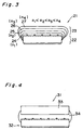
- glass layers 24 - 27 are formed in a plurality of layers so that the refractive index n increases from surface side toward outer side of a solar cell 22.
- the reflectance to solar light at the surface of a glass 23 can be reduced. Therefore, the rate of absorption of solar light by a covered solar cell 21 can be increased so that the efficiency of photoelectric conversion can be improved.
- the procedure for forming the glass 23 is similar to that shown in Fig. 2.
- the powder glass is used for the formation of the radiation protection glasses 13, 23.
- the powder glass is used for the bonding of the solar cell and the radiation protection glass.
- a radiation protection glass 33 is bonded to the surface of a solar cell 32 with a glass layer 34 formed of powder glass, by which a covered solar cell 31 is made up.
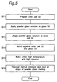
- Fig. 5 is a chart showing the procedure for bonding the glass 33 in the covered solar cell 31 having the above constitution.
- the solar cell 32 is prepared (step S11).
- a solution of powder glass is applied to the glass 33 (step S12).
- the powder glass solution is applied to the surface of the solar cell 32 (step S13).
- the solar cell 32 and the glass 33 are bonded together (step S14), and baked under high temperature and high vacuum (step S15).
- step S16 the steady pressure is recovered, followed by cooling. In this way, the radiation protection glass 33 is finally bonded.
- the glass can be formed simply by less application of the powder glass solution.
- the glass layer 34 as an adhesion layer of the solar cell 32 and the radiation protection glass 33 can be formed thinly and uniformly by a thin application of a powder glass solution to be applied. Therefore, the glass layer 34 protrudes only to a small amount, and yet the protruding glass layer 34 is superior in ultraviolet resistance, thus unnecessary to remove. Thus, the finish process after the bonding can be simplified and a cost reduction can be achieved.
- Figs. 6A, 6B, 6C and 6D show the process for forming the radiation protection glass and the electrodes according to this embodiment.
- an N+ layer 42 is formed on the surface of a P-type silicon substrate 41, and further a ground metal 43 is patterned of titanium (Ti) or the like on the N+ layer 42.
- a solution 44 obtained by dissolving powder glass in a solvent is applied overall.
- the powder glass solution 44 is repelled at ground metal 43 portions, the applied powder glass solution 44 is patterned except the ground metal 43 portions.
- the solvent is volatilized and baking process is performed, by which a glass 45 is formed as shown in Fig. 6C.
- the ground metal 43 is plated thereon with silver or the like, by which plated electrodes 46 are formed.
- the plated electrode 46 is formed only thicknesswise.
- the glass 45 formed on the surface of the N+ layer 42 is used as a pattern for the formation of the plated electrodes, there is no need for the plated electrode formation pattern made of exclusive-use resist or the like that prevents the plated electrodes 46 from laterally expanding. Also, since the formed glass 45 is patterned except the ground metal 43 portions, there is no need for alignment between the ground metal 43 and the glass 45. Therefore, it is quite easy to form the plated electrodes 46, thus making it easy to mass produce the space covered solar cell.
- the powder glass solution 44 is patterned except the surface electrode formation region.
- the present invention is not limited to this, and the powder glass solution may be patterned except the surface electrode formation region in the following fashion, as an example.
- an N+ layer is formed on the surface of the P-type silicon substrate.
- photoresist is applied overall on the P-type silicon substrate and patterned in such a way that the photoresist is left only on the surface electrode formation region.
- a solution obtained by dissolving powder glass with a solvent is applied overall on the P-type silicon substrate, and after volatilizing the solvent, the powder glass is baked, by which a radiation protection glass is formed.
- the resist is removed, and a ground metal is formed in the surface electrode formation region.
- the surface electrodes are formed by plating.
- the plated electrode are formed only thicknesswise. Further, since there is no need for alignment between the ground metal and the radiation protection glass, it is quite easy to form the plated electrodes, thus making it easy to mass produce the space covered solar cell.
- FIGs. 7A, 7B, 7C and 7D show the glass formation process according to this embodiment.
- an N+ layer 52 is formed in the surface of a P-type silicon substrate 51, and after hydrogen ions are implanted up to a peeling position (hydrogen implantation layer) 53, N electrodes 54 are formed.
- a glass 55 is formed on the N+ layer 52 side surface according to the process of any one of the first to fourth embodiments.
- heat treatment is performed, and the surface of the P-type silicon substrate 51 is peeled at the position of the hydrogen implantation layer 53 (56) as shown in Fig.
- a P electrode (not shown) is formed on the peeled surface, by which a very thin covered solar cell 57 with the radiation protection glass 55 formed therein is obtained.
- the radiation protection glass 55 serves as a reinforcement material for thin film silicon.
- an N+ layer 52' is formed and hydrogen ions are implanted up to a hydrogen implantation layer 53', after which N electrodes 54' are formed. From this onward, the steps as described above are iterated.
- the N+ layer 52 is formed on the surface of the P-type silicon substrate 51, hydrogen ions are implanted, the N electrodes 54 are formed, and thereafter the radiation protection glass 55 is formed on the N+ layer 52 side surface. After that, the peeling is performed by doing heat treatment.
- the radiation protection glass 55 can be utilized as a reinforcement material for the thin film silicon, thus eliminating the need of bonding an exclusive-use substrate for mechanical reinforcement of the thin film silicon. Therefore, a cost reduction can be achieved correspondingly.
- the radiation protection glass 55 is formed directly on the P-type silicon substrate 51 without using any adhesive, various problems involved in the case where glass is bonded with adhesive can be solved, as in the first to fourth embodiments.
- the transparent glass layer is formed directly on the surface of the solar cell, there is no need of bonding the glass plate for radiation protection to the surface of the solar cell. Therefore, the need for expensive adhesive for bonding the glass is eliminated, the work of removing overflowed adhesive is eliminated, and alignment faults between the solar cell and the glass plate are eliminated, thus allowing a cost reduction to be achieved. Further, thermal stresses on the solar cell and the glass plate due to property changes of the adhesive under low temperatures are eliminated, and thus damage of the solar cell and the glass plate or peeling of the adhesive can be reduced.
- the transparent glass layer is formed by baking powder glass. Therefore, the solution obtained by dissolving the powder glass with a solvent is applied to the surface of the solar cell and the solvent is volatilized, by which the powder glass layer is formed.
- the transparent glass layer can be formed on the surface of the solar cell easily and directly without the aid of adhesion.
- the transparent glass layer since cerium is included in the transparent glass layer, the transparent glass layer can be prevented from coloring due to radiation.
- the transparent glass layer is made up by stacking a plurality of glass layers having different refractive indices. Therefore, the optical reflectivity of the surface of the transparent glass layer can be reduced by such a setting that the plurality of glass layers making up the transparent glass layer have refractive indices increasing gradually from solar cell side toward outside. Thus, the rate of absorption of solar light can be increased so that the photoelectric conversion efficiency can be improved.
- the thickness of the transparent glass layer is 50 ⁇ m - 1000 ⁇ m. Therefore, protons of low energy, which upon collision against an object are absorbed by the very surface without reaching interior of the object, can be effectively absorbed by the transparent glass layer having a required minimum thickness.
- the transparent glass layer in the covered solar cell is formed except the surface electrode formation region. Therefore, in later process of forming the surface electrodes in the surface electrode formation region by plating, the transparent glass layer can be used as a plated electrode formation pattern, thus allowing a cost reduction to be achieved. Further, the need of alignment between the ground metal for surface electrodes and the pattern for plated electrode formation is eliminated, thus making it quite simple to form the plated electrodes and making it easy to mass produce the space covered solar cell.
- the transparent glass layer is used as an adhesion layer for bonding the radiation protection glass. Therefore, even if a thick glass is required as the glass for radiation protection, the transparent glass layer can be formed simply without using any expensive silicon adhesive. Further, since the transparent glass layer as an adhesion layer is superior in ultraviolet resistance, the work of removing overflowed transparent glass layer can be eliminated. Therefore, a cost reduction can be achieved. Further, thermal stresses on the solar cell and the glass plate due to property changes of the adhesion layer under low temperatures are eliminated, and thus damage of the solar cell and the glass plate or peeling of the adhesive can be reduced.
- a solution obtained by dissolving powder glass with a solvent is applied onto the surface of the solar cell, and after the solvent is volatilized, the powder glass is baked, by which the transparent glass layer is formed. Therefore, the transparent glass layer can be easily formed directly on the surface of the solar cell without the aid of adhesion.
- the need for any expensive adhesive is eliminated, the work of removing overflowed adhesive is eliminated, and alignment faults between the solar cell and the radiation protection glass plate are eliminated, thus allowing a cost reduction to be achieved.
- thermal stresses on the solar cell and the glass plate due to property changes of the adhesive under low temperatures are eliminated, and thus damage of the solar cell and the glass or peeling of the adhesive can be reduced.
- a PN junction is formed on the surface of a semiconductor wafer, photoresist is applied overall on the surface of the semiconductor wafer, and with the photoresist left only in the surface electrode formation region, were powder glass solution is applied overall on the semiconductor wafer. Then, the solution is volatilized and the powder glass is baked, and after removing the resist, the surface electrodes are formed by plating. Therefore, in the process of forming the surface electrodes by plating, the transparent glass layer can be exploited as a plated electrode formation pattern, thus allowing a cost reduction to be achieved. Further, since no exclusive-use plated electrode formation pattern is required, the need of alignment between the surface electrodes and the plated electrode formation pattern is eliminated, thus making it quite simple to form the plated electrodes and making it easy to mass produce the solar cell.
- a PN junction is formed on the surface of a semiconductor wafer, a ground metal is applied in a surface electrode formation region on the surface of the semiconductor wafer, and a powder glass solution is applied overall on the surface of the semiconductor wafer including the ground metal. Then, after the solution is volatilized, the powder glass is baked. Therefore, the transparent glass layer can be formed except the surface electrode formation region, and the same effects as in the foregoing embodiment can be produced. In addition to this, there is no need for patterning of photoresist for use of the transparent glass layer formation, and thus the surface electrodes can be formed even more simply than in the foregoing embodiment.
- a powder glass solution is applied onto the surface of the radiation protection glass, the powder glass solution is applied onto the surface of the solar cell, and the solar cell and the radiation protection glass are bonded together. Then, after the solvent is volatilized, the powder glass is baked. Therefore, the radiation protection glass can be bonded to the surface of the solar cell by using a transparent glass layer made of the same material as the radiation protection glass. Thus, the same effects as in an embodiment of the invention can be produced.
- a solar cell is formed by a covered solar cell manufacturing method according to any one of the foregoing embodiments, and the rear side of the semiconductor wafer in the resulting covered solar cell is peeled to a specified thickness. Therefore, in the process of manufacturing a power-saving type covered solar cell by using a thin film semiconductor substrate, the thin film semiconductor substrate can be mechanically reinforced by the transparent glass layer. Thus, the need of bonding an exclusive-use substrate for reinforcement can be eliminated, and thus problems and cost increases involved in the bonding of the exclusive-use substrate can be solved.
Landscapes
- Photovoltaic Devices (AREA)
- Electroluminescent Light Sources (AREA)
Abstract
Description
Claims (15)
- A covered solar cell in which a transparent glass layer (13, 23, 34, 45, 55) is formed directly on a surface of a solar cell (12, 22, 32).
- A covered solar cell according to Claim 1, whereinthe transparent glass layer (13, 23, 34, 45, 55) is formed by baking powder glass.
- A covered solar cell according to Claim 1, whereincerium is included in the transparent glass layer (13, 23, 34, 45, 55).
- A covered solar cell according to Claim 1, whereinthe transparent glass layer (23) is made up by stacking a plurality of glass layers (24, 25, 26, 27) having different refractive indices.
- A covered solar cell according to Claim 1, whereinthickness of the transparent glass layer (13) is 50 µm - 1000 µm.
- A covered solar cell according to Claim 1, whereinthe transparent glass layer (45) is formed except a surface electrode formation region (43).
- A covered solar cell according to Claim 1, whereinthe transparent glass layer (34) is an adhesion layer for bonding radiation protection glass (33) onto the surface of the solar cell.
- A method for manufacturing the covered solar cell as defined in Claim 2, comprising a step for forming the transparent glass layer (13, 23, 34, 45, 55) by:applying a solution of powder glass dissolved with a solvent onto the surface of the solar cell (12, 22, 32), volatilizing the solvent, and thereafter baking the powder glass.
- A method for manufacturing the covered solar cell as defined in Claim 6, comprising the steps of:forming a PN junction on a surface of a semiconductor wafer;applying photoresist overall on the surface of the semiconductor wafer, and thereafter performing a patterning so that the photoresist is left only in the surface electrode formation region;applying a solution of powder glass dissolved with a solvent overall on the surface of the semiconductor wafer, volatilizing the solvent, and thereafter baking the powder glass; andremoving the photoresist and thereafter forming surface electrodes by plating.
- A method for manufacturing the covered solar cell as defined in Claim 6, comprising the steps of:forming a PN junction on a surface of a semiconductor wafer (41);forming a ground metal (43) in the surface electrode formation region on the surface of the semiconductor wafer (41); andapplying a solution (44) of powder glass dissolved with a solvent overall on the surface of the semiconductor wafer (41) including the groundmetal (43), volatilizing the solvent, and thereafter baking the powder glass.
- A method for manufacturing the covered solar cell as defined in Claim 7, comprising the steps of:applying a solution of powder glass dissolved with a solvent onto a surface of the radiation protection glass (33);applying a solution of the powder glass dissolved with a solvent onto a surface of the solar cell (32);bonding together the solar cell and the radiation protection glass (33) at surfaces thereof onto which their corresponding solutions have been applied; andvolatilizing the solvent and thereafter baking the powder glass.
- A method for manufacturing a covered solar cell, comprising steps of:manufacturing a covered solar cell according to the covered solar cell manufacturing method as defined in Claim 8; andpeeling to a specified thickness a rear side surface of the semiconductor wafer (14) in the covered solar cell formed by the preceding step.
- A method for manufacturing a covered solar cell, comprising steps of:manufacturing a covered solar cell according to the covered solar cell manufacturing method as defined in Claim 9; andpeeling to a specified thickness a rear side surface of the semiconductor wafer in the covered solar cell formed by the preceding step.
- A method for manufacturing a covered solar cell, comprising steps of:manufacturing a covered solar cell according to the covered solar cell manufacturing method as defined in Claim 10; andpeeling to a specified thickness a rear side surface of the semiconductor wafer (41) in the covered solar cell formed by the preceding step.
- A method for manufacturing a covered solar cell, comprising steps of:manufacturing a covered solar cell according to the covered solar cell manufacturing method as defined in Claim 11; andpeeling to a specified thickness a rear side surface of the semiconductor wafer in the covered solar cell formed by the preceding step.
Applications Claiming Priority (2)
| Application Number | Priority Date | Filing Date | Title |
|---|---|---|---|
| JP16241999 | 1999-06-09 | ||
| JP16241999A JP3577430B2 (en) | 1999-06-09 | 1999-06-09 | Solar cell and method of manufacturing the same |
Publications (3)
| Publication Number | Publication Date |
|---|---|
| EP1059674A2 true EP1059674A2 (en) | 2000-12-13 |
| EP1059674A3 EP1059674A3 (en) | 2004-01-21 |
| EP1059674B1 EP1059674B1 (en) | 2013-03-27 |
Family
ID=15754251
Family Applications (1)
| Application Number | Title | Priority Date | Filing Date |
|---|---|---|---|
| EP00112306A Expired - Lifetime EP1059674B1 (en) | 1999-06-09 | 2000-06-08 | Covered solar cell and manufacturing method thereof |
Country Status (3)
| Country | Link |
|---|---|
| US (1) | US6355875B1 (en) |
| EP (1) | EP1059674B1 (en) |
| JP (1) | JP3577430B2 (en) |
Families Citing this family (13)
| Publication number | Priority date | Publication date | Assignee | Title |
|---|---|---|---|---|
| JP2003069055A (en) | 2001-06-13 | 2003-03-07 | Sharp Corp | Solar cell and method of manufacturing the same |
| JP2004127987A (en) * | 2002-09-30 | 2004-04-22 | Sharp Corp | Solar cell and method of manufacturing the same |
| JP4073890B2 (en) * | 2004-04-22 | 2008-04-09 | シャープ株式会社 | Thin film circuit board, piezoelectric speaker device and display device including the same, and sound source built-in display device |
| US7572334B2 (en) * | 2006-01-03 | 2009-08-11 | Applied Materials, Inc. | Apparatus for fabricating large-surface area polycrystalline silicon sheets for solar cell application |
| FR2896636B1 (en) * | 2006-01-20 | 2008-02-29 | Alcatel Sa | SOLAR GENERATOR HAVING A PRIMARY ELECTRIC ARC CONCENTRATOR |
| NL2000104C2 (en) * | 2006-06-15 | 2007-12-18 | Stichting Energie | Solar panel and method thereof. |
| AU2008231262B2 (en) * | 2007-03-23 | 2011-05-26 | Sunpower Corporation | Tracking solar collector assembly |
| US20080290798A1 (en) * | 2007-05-22 | 2008-11-27 | Mark Alejandro Quesada | LLT barrier layer for top emission display device, method and apparatus |
| JP5014223B2 (en) * | 2008-03-25 | 2012-08-29 | 三菱電機株式会社 | Method for manufacturing solar cell and method for manufacturing solar cell module |
| US8907202B1 (en) * | 2009-05-07 | 2014-12-09 | Scott David Brusaw | Method and system for collecting, storing and distributing solar energy using networked trafficable solar panels |
| CN102449775B (en) * | 2009-06-05 | 2014-07-02 | 独立行政法人产业技术综合研究所 | Semiconductor wafer, photoelectric conversion device, method of producing semiconductor wafer, and method of producing photoelectric conversion device |
| JP6115806B2 (en) * | 2012-11-29 | 2017-04-19 | パナソニックIpマネジメント株式会社 | Photovoltaic device |
| IT202000001051A1 (en) * | 2020-01-21 | 2021-07-21 | Cesi Centro Elettrotecnico Sperimentale Italiano Giacinto Motta S P A O In Forma Abbreviata Cesi S P | METHOD OF MANUFACTURING A SOLAR CELL WITH INTEGRAL COVERGLASS, AND CELL OBTAINED |
Family Cites Families (11)
| Publication number | Priority date | Publication date | Assignee | Title |
|---|---|---|---|---|
| US3247428A (en) * | 1961-09-29 | 1966-04-19 | Ibm | Coated objects and methods of providing the protective coverings therefor |
| US3653970A (en) * | 1969-04-30 | 1972-04-04 | Nasa | Method of coating solar cell with borosilicate glass and resultant product |
| US4262161A (en) * | 1980-01-16 | 1981-04-14 | Shell Oil Company | Covered solar cell assembly |
| FR2488447A1 (en) * | 1980-08-06 | 1982-02-12 | Comp Generale Electricite | PROCESS FOR MANUFACTURING PHOTOVOLTAIC CELL MODULES |
| GB8623214D0 (en) * | 1986-09-26 | 1986-10-29 | Pilkington Brothers Plc | Glass compositions |
| JPH03126063A (en) | 1989-10-11 | 1991-05-29 | Brother Ind Ltd | cleaning equipment |
| JPH03126063U (en) | 1990-04-03 | 1991-12-19 | ||
| JP3126063B2 (en) | 1992-02-21 | 2001-01-22 | 富士薬品工業株式会社 | Method for producing D-pantolactone |
| EP0638939A3 (en) * | 1993-07-19 | 1997-08-20 | Matsushita Electric Industrial Co Ltd | Solar cell with a low-melting layer of glass. |
| JPH07169986A (en) | 1993-12-14 | 1995-07-04 | Bridgestone Corp | Amorphous solar cell sealing method |
| JPH1093122A (en) | 1996-09-10 | 1998-04-10 | Nippon Telegr & Teleph Corp <Ntt> | Manufacturing method of thin film solar cell |
-
1999
- 1999-06-09 JP JP16241999A patent/JP3577430B2/en not_active Expired - Fee Related
-
2000
- 2000-06-07 US US09/588,688 patent/US6355875B1/en not_active Expired - Lifetime
- 2000-06-08 EP EP00112306A patent/EP1059674B1/en not_active Expired - Lifetime
Also Published As
| Publication number | Publication date |
|---|---|
| JP2000349310A (en) | 2000-12-15 |
| JP3577430B2 (en) | 2004-10-13 |
| US6355875B1 (en) | 2002-03-12 |
| EP1059674A3 (en) | 2004-01-21 |
| EP1059674B1 (en) | 2013-03-27 |
Similar Documents
| Publication | Publication Date | Title |
|---|---|---|
| EP1059674B1 (en) | Covered solar cell and manufacturing method thereof | |
| US4754544A (en) | Extremely lightweight, flexible semiconductor device arrays | |
| US4416052A (en) | Method of making a thin-film solar cell | |
| US8106290B2 (en) | Method for manufacturing single crystal silicon solar cell and single crystal silicon solar cell | |
| US7098395B2 (en) | Thin-film solar cell module of see-through type | |
| CN105684165B (en) | Solar cell and its manufacture method and solar module | |
| EP3664157B1 (en) | Solar cell and method for manufacturing the same | |
| JP2001189480A (en) | Method of manufacturing solar cell | |
| JP2001189475A (en) | Method of manufacturing solar cell | |
| US20100216276A1 (en) | Method for Electrically Connecting Photovoltaic Cells in a Photovoltaic Device | |
| JP2001189481A (en) | Method of manufacturing solar cell | |
| JP2001189482A (en) | Method of manufacturing solar cell | |
| JPS63232376A (en) | Method for manufacturing photovoltaic devices | |
| US9263603B2 (en) | Solar cell with connecting sheet, solar cell module, and fabrication method of solar cell with connecting sheet | |
| EP0007669B1 (en) | The manufacture of an infra-red detector element, and detector elements so manufactured | |
| EP3025192B1 (en) | Electrochromic devices having improved structure for reducing current leakage across portions of the lower transparent conductor layer | |
| CN101432888B (en) | Ultra lightweight photovoltaic device and method for its manufacture | |
| GB1575888A (en) | Solar cell array | |
| EP0189976A2 (en) | Extremely lightweight, flexible semiconductor device arrays and method of making same | |
| US8841161B2 (en) | Method for forming flexible solar cells | |
| CN118522783A (en) | A solar cell and a method for preparing the same | |
| JP3854977B2 (en) | Method for manufacturing solar battery cell | |
| JP3419108B2 (en) | Manufacturing method of thin film solar cell | |
| EP0457312B1 (en) | Photovoltaic device useful as a mirror | |
| EP4156306A1 (en) | Lightweight flexible solar array |
Legal Events
| Date | Code | Title | Description |
|---|---|---|---|
| PUAI | Public reference made under article 153(3) epc to a published international application that has entered the european phase |
Free format text: ORIGINAL CODE: 0009012 |
|
| AK | Designated contracting states |
Kind code of ref document: A2 Designated state(s): AT BE CH CY DE DK ES FI FR GB GR IE IT LI LU MC NL PT SE |
|
| AX | Request for extension of the european patent |
Free format text: AL;LT;LV;MK;RO;SI |
|
| PUAL | Search report despatched |
Free format text: ORIGINAL CODE: 0009013 |
|
| AK | Designated contracting states |
Kind code of ref document: A3 Designated state(s): AT BE CH CY DE DK ES FI FR GB GR IE IT LI LU MC NL PT SE |
|
| AX | Request for extension of the european patent |
Extension state: AL LT LV MK RO SI |
|
| RIC1 | Information provided on ipc code assigned before grant |
Ipc: 7H 01L 31/18 B Ipc: 7H 01L 31/048 B Ipc: 7H 01L 31/0216 A |
|
| 17P | Request for examination filed |
Effective date: 20040617 |
|
| AKX | Designation fees paid |
Designated state(s): DE FR |
|
| 17Q | First examination report despatched |
Effective date: 20041112 |
|
| GRAP | Despatch of communication of intention to grant a patent |
Free format text: ORIGINAL CODE: EPIDOSNIGR1 |
|
| GRAP | Despatch of communication of intention to grant a patent |
Free format text: ORIGINAL CODE: EPIDOSNIGR1 |
|
| GRAS | Grant fee paid |
Free format text: ORIGINAL CODE: EPIDOSNIGR3 |
|
| GRAA | (expected) grant |
Free format text: ORIGINAL CODE: 0009210 |
|
| AK | Designated contracting states |
Kind code of ref document: B1 Designated state(s): DE FR |
|
| REG | Reference to a national code |
Ref country code: DE Ref legal event code: R096 Ref document number: 60047908 Country of ref document: DE Effective date: 20130523 |
|
| PGFP | Annual fee paid to national office [announced via postgrant information from national office to epo] |
Ref country code: DE Payment date: 20130626 Year of fee payment: 14 |
|
| PGFP | Annual fee paid to national office [announced via postgrant information from national office to epo] |
Ref country code: FR Payment date: 20130726 Year of fee payment: 14 |
|
| PLBE | No opposition filed within time limit |
Free format text: ORIGINAL CODE: 0009261 |
|
| STAA | Information on the status of an ep patent application or granted ep patent |
Free format text: STATUS: NO OPPOSITION FILED WITHIN TIME LIMIT |
|
| 26N | No opposition filed |
Effective date: 20140103 |
|
| REG | Reference to a national code |
Ref country code: DE Ref legal event code: R097 Ref document number: 60047908 Country of ref document: DE Effective date: 20140103 |
|
| REG | Reference to a national code |
Ref country code: DE Ref legal event code: R119 Ref document number: 60047908 Country of ref document: DE |
|
| REG | Reference to a national code |
Ref country code: DE Ref legal event code: R119 Ref document number: 60047908 Country of ref document: DE Effective date: 20150101 |
|
| REG | Reference to a national code |
Ref country code: FR Ref legal event code: ST Effective date: 20150227 |
|
| PG25 | Lapsed in a contracting state [announced via postgrant information from national office to epo] |
Ref country code: DE Free format text: LAPSE BECAUSE OF NON-PAYMENT OF DUE FEES Effective date: 20150101 |
|
| PG25 | Lapsed in a contracting state [announced via postgrant information from national office to epo] |
Ref country code: FR Free format text: LAPSE BECAUSE OF NON-PAYMENT OF DUE FEES Effective date: 20140630 |