The present invention relates to a semiconductor
memory and a method of operating a semiconductor memory.
Description of the Prior Art
In recent years, a nonvolatile semiconductor memory
such as an EPROM (erasable and programmable read only
memory) or an EEPROM (electrically erasable and
programmable read only memory) is watched with interest as
a semiconductor memory capable of substituting for a hard
disk or a floppy disk serving as a magnetic memory.
In a memory cell of an EPROM or an EEPROM, carriers
are stored in a floating gate electrode for storing data
by presence/absence of the carriers and reading data by
detecting change of a threshold voltage following
presence/absence of carriers. In particular, the EEPROM
includes a flash EEPROM erasing data in a memory cell
array as a whole or dividing the memory cell array into
arbitrary blocks and erasing data in units of the
respective blocks. The flash EEPROM, also referred to as a
flash memory, capable of attaining a large capacity, low
power consumption,and a high-speed operation with
excellent impact resistance is applied to various types of
portable apparatuses. Further, the flash EEPROM having
memory cells each formed by a single transistor can be
readily integrated as compared with the EEPROM.
In general, a stacked gate memory cell and a split
gate memory cell are proposed for forming the flash EEPROM.
In a write operation of storing electrons in a
floating gate electrode of the stacked gate memory cell,
electrons contained in a channel of a semiconductor
substrate are converted to hot electrons and injected into
the floating gate electrode. At this time, a voltage of
ten-odd volts must be applied to a control gate electrode.
In an erase operation of extracting electrons stored in
the floating gate electrode of the stacked gate memory
cell, a Fowler-Nordheim tunnel current (hereinafter
referred to as an FN tunnel current) is fed from a drain
region to the floating gate electrode. At this time, a
voltage of ten-odd volts must be applied to the drain
region.
In a write operation of storing electrons in a
floating gate electrode of the split gate memory cell,
electrons contained in a channel of a semiconductor
substrate are converted to hot electrons and injected into
the floating gate electrode. At this time, a voltage of
ten-odd volts must be applied to a drain region. In an
erase operation of extracting electrons stored in the
floating gate electrode of the split gate memory cell, an
FN tunnel current is fed from a control gate electrode to
the floating gate electrode. At this time, a voltage of
ten-odd volts must be applied to the control gate
electrode.
Thus, in the conventional stacked gate or split gate
memory cell, electrons are injected into the floating gate
electrode as hot electrons in the write operation, and the
electrons stored in the floating gate electrode are
extracted through the FN tunnel current in the erase
operation.
In order to hold carriers stored in the floating gate
electrode over a long period of time, the thickness of an
insulator film enclosing the floating gate electrode must
be increased. However, the electrons are injected into or
extracted from the floating gate electrode as hot
electrons or through the FN tunnel current. Therefore, the
voltage (hereinafter referred to as the operating voltage
of the memory cell) applied to the control gate electrode
or the drain region in the write or erase operation must
be increased as the thickness of the insulator film
enclosing the floating gate electrode is increased.
A step-up circuit generates the operating voltage of
the memory cell. In this case, the step-up circuit can
practically generate a voltage of up to ten-odd volts.
When employing a silicon oxide film as the insulator film
enclosing the floating gate electrode, the thickness of
this silicon oxide film cannot exceed 8 to 10 nm assuming
that the operating voltage of the memory cell is ten-odd
volts. In general, therefore, the thickness of the silicon
oxide film employed as the insulator film enclosing the
floating gate electrode is set to 8 to 10 nm, in order to
suppress the operating voltage of the memory cell to ten-odd
volts. When the thickness of the silicon oxide film is
about 8 to 10 nm, electrons stored in the floating gate
electrode can be held for a period practically
satisfactory to some extent.
Also when storing holes in the floating gate
electrode, the thickness of the silicon oxide film forming
the insulator film enclosing the floating gate electrode
is set to 8 to 10 nm similarly to the aforementioned case
of storing electrons, thereby suppressing the operating
voltage of the memory cell to ten-odd volts and holding
the holes stored in the floating gate electrode for a
period practically satisfactory to some extent.
The feature of the flash memory resides in that cells
sharing a word line are temporarily subjected to batch
erasing and thereafter subjected to rewriting. In relation
to the memory cell array, a structure operable with a
small number of contacts is employed in order to improve
the degree of integration.
Recently, the flash EEPROM is also required to attain
a lower voltage, operations at a higher speed, lower power
consumption and higher integration while attaining a
longer life by increasing the period for holding carriers
stored in the floating gate electrode.
When forming the insulator film enclosing the
floating gate electrode by the silicon oxide film having
the thickness generally set to 8 to 10 nm as described
above, the thickness of the silicon oxide film must not be
reduced below 8 nm, in order to attain a long life.
When reducing the operating voltage of the memory
cell, the time (lead time) for stepping up the voltage is
so reduced that the write and erase operations can be
performed at a higher speed. Further, power consumption
can also be reduced.
The circuit scale of the step-up circuit for
generating the operating voltage of the memory cell is
increased as the generated voltage is increased. The
occupied area (transistor size) of a transistor forming a
peripheral circuit, such as a decoder, a sense amplifier
or a buffer, of the flash EEPROM is increased on the
substrate as the voltage resistance thereof is increased.
When reducing the operating voltage of the memory cell,
therefore, the circuit scale of the step-up circuit as
well as the size of the transistor forming the peripheral
circuit are reduced, whereby higher integration can be
attained.
Thus, operations at a higher speed, lower power
consumption and higher integration can be simultaneously
implemented by reducing the operating voltage of the
memory cell.
In the conventional stacked gate or split gate memory
cell, however, electrons are injected into or extracted
from the floating gate electrode as hot electrons or
through the FN tunnel current. When employing the silicon
oxide film as the insulator film enclosing the floating
gate electrode, therefore, it is difficult to reduce the
operating voltage of the memory cell beyond the current
level while maintaining the thickness of the silicon oxide
film at the current level of 8 to 10 nm. In other words,
it is difficult to reduce the operating voltage of the
memory cell while keeping the life of the conventional
stacked gate or split gate memory cell at the current
level without changing the structure thereof.
As described above, the feature of the flash memory
resides in that the cells sharing a word line are
subjected to batch erasing and thereafter subjected to
rewriting. Therefore, the cells sharing the word line must
be subjected to erasing and writing also when data may not
be rewritten. In this case, the data are rewritten in two
stages of erasing and writing. Therefore, it is difficult
to perform writing on a group of cells forming a block
(sector) subjected to batch erasing simultaneously with
batch erasing or to perform the so-called overwriting
performed in a magnetic disk. Thus, it is difficult to
increase the speed for write and erase operations.
An object of the present invention is to provide a
semiconductor memory capable of attaining a longer life, a
lower voltage, operations at a higher speed, lower power
consumption and a higher degree of integration.
Another object of the present invention is to
implement the aforementioned semiconductor memory in a
simple structure.
Still another object of the present invention is to
further refine a first gate electrode and a second gate
electrode and suppress dispersion of the gate lengths in
the aforementioned semiconductor memory.
A further object of the present invention is to
simultaneously perform erasing and writing in the
aforementioned semiconductor memory.
A further object of the present invention is to
provide a method of operating a semiconductor memory
capable of readily operating the aforementioned
semiconductor memory.
A semiconductor memory according to a first aspect of
the present invention comprises a first gate electrode, a
second gate electrode, a semiconductor region, a first
insulator film formed on one surface of the semiconductor
region and a second insulator film formed on another
surface of the semiconductor region, for injecting
carriers into the second gate electrode through the first
insulator film, the semiconductor region and the second
insulator film. In this case, the semiconductor region is
preferably formed by a second conductivity type impurity
region formed on a first layer consisting of a first
conductivity type semiconductor. Preferably, the
semiconductor region includes a second conductivity type
semiconductor film formed on a first layer consisting of a
first conductivity type semiconductor. In this case, the
first gate electrode and the second gate electrode may be
formed in a self-aligned manner.
A semiconductor memory according to a second aspect
of the present invention comprises a second conductivity
type first region and a second conductivity type second
region formed on a first layer consisting of a first
conductivity type semiconductor, a first gate electrode
and a second gate electrode formed on the first layer
between the first region and the second region, a second
conductivity type third region formed on the first layer
between the first gate electrode and the second gate
electrode, a first insulator film formed between the first
gate electrode and the third region and a second insulator
film formed between the second gate electrode and the
third region.
According to the present invention, therefore, the
potential of the third region can be increased by simply
applying a prescribed voltage to the second region for
readily generating an electric field between the third
region and the first gate electrode. Consequently,
carriers permeating through a barrier of the insulator
film located between the first gate electrode and the
third region are accelerated by the electric field
generated in the third region, to be injected into and
stored in the second gate electrode beyond a barrier of
the insulator film located between the third region and
the second gate electrode. Therefore, data can be stored
by presence/absence of carriers stored in the second gate
electrode, and the semiconductor memory operates as a
nonvolatile semiconductor memory.
In the aforementioned semiconductor memory according
to the second aspect, the third region is preferably
formed by a second conductivity type impurity region.
Further, the third region may include a second
conductivity type conductive film. In this case, the first
gate electrode and the second gate electrode are
preferably formed in a self-aligned manner.
It is preferable that the first gate electrode is
formed through a first gate insulator film with respect to
the first layer, and the second gate electrode is formed
through a second gate insulator film with respect to the
first layer.
It is preferable that the electrostatic capacitance
between the second region and the second gate electrode is
set larger than the electrostatic capacitance between the
third region and the second gate electrode, and a voltage
applied to the second region is transmitted to the second
gate electrode by electrostatic coupling between the
second region and the second gate electrode so that the
third region connected with the second region through the
first layer is substantially equalized in potential with
the second region. Thus, the potential of the second gate
electrode can be readily controlled by simply controlling
the potential of the second region.
The width of the third region is preferably set
substantially not more than the mean free path of carriers
permeating through a barrier of the first insulator film
located between the first gate electrode and the third
region when having energy necessary for passing through a
barrier of the second insulator film.
Thus, substantially all carriers permeating through
the barrier of the first insulator film located between
the first gate electrode and the third region acquire the
energy for passing through the barrier of the second
insulator film and turn into hot carriers, to be injected
into the second gate electrode in an extremely high
probability without remaining in the third region. Thus,
the aforementioned functions of the present invention can
be more reliably attained.
The second gate electrode is preferably formed on the
side wall of the second region through a third insulator
film. Thus, the areas of the overlapping portions of the
second region and the second gate electrode can be readily
increased for consequently increasing the electrostatic
capacitance between the second region and the second gate
electrode.
In this case, a groove may be formed in the first
layer so that the second gate electrode is formed in the
groove through the third insulator film on the side of the
second region. Thus, the second gate electrode can be
readily formed on the side wall of the second region.
In the aforementioned semiconductor memory according
to the second aspect, it is preferable that a first
conductivity type fourth region is formed on the second
conductivity type second region, and the second region is
formed on the overall region between the first layer and
the fourth region.
Thus, the second region and the fourth region form a
diode, so that a negative voltage can be readily applied
to the second region and the fourth region having the
diode structure without employing a complicated structure
such as a conventional triple well structure. Therefore,
positive and negative voltages can be employed for erase
and write operations, and hence the maximum voltage
generated in a step-up circuit can be substantially halved.
Thus, voltage reduction can be attained and the scale of
the step-up circuit can also be reduced, whereby higher
integration can be attained. Further, the fourth region
can be readily formed through a general process of
implanting impurity ions, to result in no burden in the
process.
There is a possibility that an excess current flows
between the second region and the first layer when
applying a negative voltage to the second region without
employing the inventive diode structure, while an excess
current may flow also between the first region and the
second region (between a source and a drain) after erasing
when either the first region or the second region is not
floated after erasing. In this case, the excess current
may disadvantageously exceed the allowable current
quantity in the step-up circuit. According to the present
invention, flow of such an excess current can be
effectively prevented by employing the diode structure.
In this case, the fourth region is preferably
capacitively coupled with the second gate electrode
through a third insulator film. Thus, the voltage of the
fourth region, which is directly applied from a power
source through a wire, can be efficiently transmitted to
the second gate electrode by capacitive coupling.
In the aforementioned semiconductor memory according
to the second aspect, the first gate electrode preferably
includes a side wall film formed in a self-aligned manner
with respect to the third region. Thus, the first gate
electrode can be formed with no problem of misalignment of
a mask in a mask process.
In this case, the side wall film is preferably formed
by depositing a first conductive film on the side surface
of the third region and thereafter etching back the first
conductive film. Thus, the gate length of the first gate
electrode can be controlled through the thickness of the
first conductive film, whereby the gate length can be
reduced below the minimum limit size (minimum exposure
size) in the mask process and controlled in higher
precision than that in the mask process. Consequently, the
first gate electrode can be more refined and dispersion of
the gate length can be suppressed.
Preferably, the aforementioned semiconductor memory
according to the second aspect further comprises a wire
connected to the first region, and the wire is formed in a
self-aligned manner with respect to the first region. Thus,
the wire can be formed with no problem of misalignment of
a mask in a mask process.
In this case, the wire is preferably formed by
depositing a second conductive film on the side surface of
the first gate electrode through a fourth insulator film
and thereafter etching back the second conductive film.
Thus, a wire insulated from the first gate electrode can
be readily formed on the side portion of the first gate
electrode in a self-aligned manner.
In the aforementioned semiconductor memory according
to the second aspect, the third region is preferably
formed by forming a side wall insulator film on the side
surface of the first gate electrode in a self-aligned
manner and thereafter etching back the first layer through
the side wall insulator film. Thus, the third region can
be formed in a self-aligned manner through the side wall
insulator film formed in a self-aligned manner with no
problem of misalignment of a mask in a mask process.
Further, the third region can be formed in a small width
below the minimum limit size in the mask process by
controlling the thickness of the insulator film for
forming the side wall insulator film. In addition, the
width of the side wall insulator film can be precisely
controlled by controlling the thickness of the insulator
film for forming the side wall insulator film, whereby the
width of the third region formed through the side wall
insulator film can also be precisely controlled.
Consequently, the third region can be more refined and
dispersion of the width of the third region can be
suppressed.
It is preferable that the first gate electrode and
the second gate electrode are formed on the major surface
of the first layer and the third region consisting of the
conductive film is formed between the first gate electrode
and the second gate electrode on the major surface of the
first layer. When forming the first gate electrode, the
second gate electrode and the third region on the first
layer in the aforementioned manner, no grooves may be
formed in the first layer for embedding the first gate
electrode, the second gate electrode and the third region.
Therefore, the structure can be simplified as compared
with the case of forming such grooves, and the inventive
semiconductor memory can consequently be implemented in a
simple structure. Further, the first layer may not be
formed with grooves and hence the structure having the
first gate electrode, the third region and the second gate
electrode can be formed through a simple process. In
addition, no tunnel insulator film or the like may be
formed on the side surface of the first layer damaged by
etching for forming such grooves, whereby the quality of a
tunnel insulator film is not deteriorated.
In this case, it is preferable that at least part of
the third region is formed on the upper surface of the
second gate electrode, and at least part of the first gate
electrode is formed on the upper surface of the third
region. Thus, a structure requiring no grooves in the
first layer can be readily obtained by vertically
arranging the first gate electrode, the second gate
electrode and the third region.
The third region preferably includes a single-crystalline
silicon film. Thus, the first insulator film
can be formed by oxidizing the single-crystalline silicon
film, whereby the first insulator film can be obtained
with excellent film quality.
The third region may include a first side wall film
consisting of a first conductive film formed in a self-aligned
manner. Thus, the third region consisting of the
first conductive film can be formed with no problem of
misalignment of a mask in a mask process.
In this case, the first side wall film consisting of
the first conductive film preferably includes a second
side wall film consisting of a second conductive film
formed on the side wall of the second gate electrode
through the second insulator film and a third side wall
film consisting of a third conductive film formed to be in
contact with the side surface of the second side wall film
and the surface of the first layer. Thus, the third side
wall film can connect the third region and the first layer
with each other thereby connecting the third region with
the second region through the first layer. Thus, the
aforementioned functions of the present invention can be
more reliably attained.
In this case, it is preferable that the second side
wall film is formed by depositing a second conductive film
on the side surface of the second gate electrode through
the second insulator film and thereafter etching back the
second conductive film, and the third side wall film is
formed by depositing a third conductive film to cover the
first layer and the second side wall film and thereafter
etching back the third conductive film, to be in contact
with the side surface of the second side wall film and the
surface of the first layer.
Thus, the thicknesses of the second side wall film
and the third side wall film can be controlled by the
thicknesses of the second conductive film and the third
conductive film respectively, whereby the third region
consisting of the second side wall film and the third side
wall film can be formed in a small width below the minimum
limit size (minimum exposure size) in the mask process.
Further, the widths of the second and third side wall
films can be precisely controlled by controlling the
widths of the second and third conductive films, whereby
the width of the third region consisting of the second and
third side wall films can also be precisely controlled.
Consequently, the third region can be more refined and
dispersion of the width of the third region can be
suppressed.
The second region preferably includes a fourth side
wall film consisting of a fourth conductive film formed on
the side surface of the second gate electrode in a self-aligned
manner through a third insulator film. Thus, the
fourth side wall film can increase the opposite areas of
the second region and the second gate electrode. Therefore,
the electrostatic capacitance between the second region
and the second gate electrode can be readily increased.
Consequently, the electrostatic capacitance between the
second region and the second gate electrode can be readily
increased beyond the electrostatic capacitance between the
third region and the second gate electrode. Therefore, the
potential of the second gate electrode can be readily
controlled by varying the voltage applied to the second
region.
In this case, the fourth side wall film preferably
includes a fifth side wall film consisting of a fifth
conductive film formed on the side wall of the second gate
electrode through the third insulator film and a sixth
side wall film consisting of a sixth conductive film
formed to be in contact with the side surface of the fifth
side wall film and the surface of the first layer. Thus,
the sixth side wall film enables connection with the first
layer, whereby the fifth and sixth side wall films can be
readily connected with the second region consisting of the
impurity region formed on the first layer. Consequently,
the fifth and sixth side wall films can be readily
employed as part of the second region.
The fourth side wall film defining the second region
is preferably formed simultaneously with the first side
wall film defining the third region. Thus, the fabrication
process is not complicated also when providing the fourth
side wall film.
It is preferable that the first region and the second
region are so formed on the first layer as to expose the
side surfaces thereof, the first gate electrode includes a
seventh side wall film formed on the side surface of the
first region in a self-aligned manner through a third
insulator film, and the second gate electrode includes an
eighth side wall film formed on the side surface of the
second region in a self-aligned manner through a fourth
insulator film.
Thus, the gate lengths of the first gate electrode
and the second gate electrode can be controlled by the
thickness of the deposited conductive film and hence the
gate lengths can be reduced below the minimum limit size
(minimum exposure size) in a mask process and controlled
in higher precision than that in the mask process.
Consequently, the first gate electrode and the second gate
electrode can be more refined and dispersion of the gate
lengths can be suppressed.
In this case, the seventh side wall film and the
eighth side wall film are preferably simultaneously formed
by depositing a seventh conductive film to cover the
overall surface and thereafter etching back the seventh
conductive film. Thus, the first gate electrode and the
second gate electrode are simultaneously formed so that
the fabrication process can be simplified.
The third region consisting of the conductive film
may be formed in a self-aligned manner with respect to the
first gate electrode and the second gate electrode. Thus,
the third region can be formed in addition to the first
gate electrode and the second gate electrode with no
problem of misalignment of a mask in a mask process.
In this case, the third region is preferably formed
to fill up a clearance between the seventh side wall film
and the eighth side wall film. Thus, the third region can
be readily formed in a self-aligned manner.
The thickness of the first insulator film is
preferably smaller than the thickness of the second
insulator film. Thus, a barrier of the first insulator
film on the side of the first gate electrode for
extracting carriers can be reduced in thickness for
readily extracting the carriers from the first gate
electrode. Further, the carriers stored in the second gate
electrode can be held over a long period of time with the
thick second insulator film on the side of the second gate
electrode.
In this case, the first insulator film and the second
insulator film are preferably formed by introducing an
impurity suppressing oxidation into the first gate
electrode while introducing an impurity prompting
oxidation into the second gate electrode and thereafter
oxidizing the first gate electrode and the second gate
electrode respectively. Thus, the second insulator film
and the first insulator film having a smaller thickness
than the second insulator film can be simultaneously
formed through a single oxidation step.
Preferably, a fifth insulator film is formed between
the upper surface of the third region located between the
first gate electrode and the second gate electrode and the
upper side surfaces of the first gate electrode and the
second gate electrode. Thus, the fifth insulator film can
reliably insulate the first gate electrode and the second
gate electrode from the third region.
A semiconductor memory according to a third aspect of
the present invention comprises a second conductivity type
region formed on a first layer consisting of a first
conductivity type semiconductor, a gate electrode and a
semiconductor region formed between the second
conductivity type region and the gate electrode through
insulator films respectively. Carriers are injected into
the gate electrode from the second conductivity type
region through the insulator films and the semiconductor
region. The operation of injecting carriers includes not
only injection of electrons but also extraction of
electrons. In this case, the semiconductor region
preferably consists of a second conductivity type impurity
region formed on the first layer consisting of the first
conductivity type semiconductor.
A semiconductor memory according to a fourth aspect
of the present invention comprises a second conductivity
type first region and a second conductivity type second
region formed on a first layer consisting of a first
conductivity type semiconductor, a first gate electrode
formed on the first layer, a second gate electrode formed
on the first layer between the first region and the second
region, a second conductivity type third region formed
between either the first gate electrode or the second
region on the first layer and the second gate electrode, a
first insulator film formed on one surface of the third
region and a second insulator film formed on another
surface of the third region.
According to the present invention, therefore, the
potential of the third region can be increased by applying
a prescribed voltage to the first gate electrode or the
second region thereby readily generating an electric field
between the third region and the first gate electrode or
the second region. Consequently, carriers permeating
through a barrier of the insulator film located between
the first gate electrode or the second region and the
third region are accelerated by the electric field
generated in the third region to be injected into (written
in) and stored in the second gate electrode through the
barrier of the insulator film located between the third
region and the second gate electrode. Therefore, data can
be stored by presence/absence of the carriers stored in
the second gate electrode, and the semiconductor memory
operates as a nonvolatile semiconductor memory.
In this case, it is preferable that the semiconductor
memory further comprises a third insulator film formed
between the second gate electrode and the first region,
the first gate electrode extends in a direction
intersecting with the first region and the second region,
the first insulator film is formed between the third
region and the second region, and the second insulator
film is formed between the third region and the second
gate electrode. This structure is hereinafter referred to
as a structure 1.
When employing the structure 1, the potential of the
third region can be increased by applying a positive
voltage to the first region and the first gate electrode
and a negative voltage to the second region, thereby
readily generating an electric field between the third
region and the second region. Consequently, carriers
permeating through a barrier of the first insulator film
located between the second region and the third region are
accelerated by the electric field generated in the third
region to be injected into (written in) and stored in the
second gate electrode through the barrier of the second
insulator film located between the third region and the
second gate electrode. Therefore, data can be stored by
presence/absence of the carriers stored in the second gate
electrode, and the semiconductor memory operates as a
nonvolatile semiconductor memory. As to a memory cell
subjected to erasing, a negative voltage is applied to the
first gate electrode thereby extracting the electrons
stored in the second gate electrode toward the first
region for performing erasing.
According to this structure 1, write and erase
operations can be controlled only with a positive/negative
voltage applied to the first gate electrode. Thus, batch
rewriting is enabled for simultaneously performing erasing
and writing on about 1000 to 4000 memory cells connected
to a plurality of first gate electrodes respectively,
which are subjected to writing after batch erasing in the
conventional flash memory.
In the aforementioned semiconductor memory according
to the structure 1, the second gate electrode is
preferably formed through a gate insulator film with
respect to the first layer. Thus, the second gate
electrode can be operated as the gate of a transistor in
the write operation.
In the aforementioned semiconductor memory according
to the structure 1, the electrostatic capacitance between
the first gate electrode and the second gate electrode is
set larger than the electrostatic capacitance of the
remaining parts, and a voltage applied to the first gate
electrode is transmitted to the second gate electrode by
electrostatic coupling between the first gate electrode
and the second gate electrode so that the third region
connected with the first region through the first layer is
substantially equalized in potential with the first region.
Thus, the potential of the second gate electrode can be
readily controlled by simply controlling the potential of
the first gate electrode.
In the aforementioned semiconductor memory according
to the structure 1, the third region and the second region
are preferably connected through a diode such as a p-n
junction diode or a Schottky barrier diode. Thus, the
potential difference between the second region and the
third region can be held when a negative voltage is
applied to the second region and a positive or ground
voltage is transmitted to the third region in writing.
When a positive voltage is applied to the second region in
reading, on the other hand, a current can be fed between
the second region and the third region with no or low
resistance.
In the aforementioned semiconductor memory according
to the structure 1, the second region may include a
material having a Schottky barrier with respect to silicon.
Thus, potential difference is held between the third
region and the second region due to the Schottky barrier,
whereby electrons can be accelerated. Further, the
Schottky barrier has a relatively low level of about 0.5
eV, and hence a large quantity of electrons can be
extracted from the second region also when the potential
difference between the second and third regions is small.
In this case, the first insulator film preferably has the
smallest possible thickness within the range stabilizing
the interface between the second region and the third
region. Thus, the thickness of a barrier formed by the
first insulator film can be reduced by reducing the
thickness of the first insulator film, so that the first
insulator film can be prevented from influencing the
Schottky barrier characteristic. At the same time, the
first insulator film can readily stabilize the interface
between the second region and the third region readily
unstabilized due to generation of a large number of
interfacial levels.
The thickness of the Schottky barrier can be
precisely controlled with the impurity concentration of
the third region. In this case, a potential gradient can
be provided on the third region by lowering the impurity
concentration of the third region. Thus, the electrons
extracted from the second region can be gradually
accelerated and supplied with energy for passing through a
barrier of an oxide film immediately before injection into
the second gate electrode. Thus, the electrons are
transported to a portion close to the second gate
electrode in a low energy state with a long mean free path
and further accelerated to be injected into the second
gate electrode, to hardly lose energy in the course of the
process. Consequently, the electrons are injected into the
second gate electrode with a high probability.
In this case, an insulator film located between the
second region and the first layer preferably has a
thickness capable of insulating the second region and the
first layer from each other. Thus, also when the third
region and the second region are reverse-biased through
the Schottky barrier and the second region and the first
layer are forward-biased, the insulator film can
sufficiently insulate the second region and the first
layer from each other.
In the aforementioned semiconductor memory according
to the structure 1, the width of the third region is
preferably set substantially not more than the mean free
path of carriers permeating through a barrier of the first
insulator film located between the second region and the
third region when having energy necessary for passing
through a barrier of the second insulator film. Thus,
almost all carriers permeating through the barrier of the
first insulator film located between the second region and
the third region acquire energy for passing through the
barrier of the second insulator film and turn into hot
carriers, to be injected into the second gate electrode in
an extremely high probability without remaining in the
third region. Therefore, the aforementioned functions of
the present invention can be more reliably attained.
A method of operating a semiconductor memory
according to a fifth aspect of the present invention is a
method of operating a semiconductor memory comprising a
second conductivity type first region and a second
conductivity type second region formed on a first layer
consisting of a first conductivity type semiconductor, a
first gate electrode formed on the first layer between the
first region and the second region through a first gate
insulator film with respect to the first layer, a second
gate electrode formed on the first layer between the first
region and the second region through a second gate
insulator film with respect to the first layer, a second
conductivity type third region formed on the first layer
between the first gate electrode and the second gate
electrode, a first insulator film formed between the first
gate electrode and the third region and a second insulator
film formed between the second gate electrode and the
third region, for writing data by injecting hot carriers
into the second gate electrode from the first gate
electrode through the first insulator film, the third
region and the second insulator film.
In an initial stage of a write operation, prescribed
potential difference is caused between the first gate
electrode and the third region and between the first gate
electrode and the second gate electrode, for continuously
performing writing. Hot carriers are continuously injected
into the second gate electrode as the write operation
progresses, so that the potential of the second gate
electrode gradually lowers from the initial value. The
potential of the third region also lowers along with
reduction of the potential of the second gate electrode,
so that the potential difference between the first gate
electrode and the third region finally lowers below a
prescribed value. Thus, the hot carriers contained in the
first gate electrode cannot permeate through the barrier
of the second insulator film even if the hot carriers
contained in the first gate electrode can permeate through
the barrier of the first insulator film, to automatically
terminate the write operation.
In the aforementioned method of operating a
semiconductor device according to the fifth aspect, data
of at least three values may be written by varying the
initial field intensity between the first gate electrode
and the third region thereby controlling the quantity of
the hot carriers injected into the second gate electrode.
Thus, multivalued data can be stored in a single
semiconductor memory.
It is preferable to erase data by extracting the hot
carriers from the second gate electrode to the third
region through the second insulator film.
The electrostatic capacitance between the second
region and the second gate electrode is preferably set
larger than the electrostatic capacitance between the
third region and the second gate electrode, and a voltage
applied to the second region is preferably transmitted to
the second gate electrode by electrostatic coupling
between the second region and the second gate electrode so
that the third region connected with the second region
through the first layer is substantially equalized in
potential with the second region. Thus, the potential of
the second gate electrode can be readily controlled by
simply controlling the potential of the second region.
The width of the third region is preferably set
substantially not more than the mean free path of carriers
permeating through a barrier of the first insulator film
located between the first gate electrode and the third
region when having energy necessary for passing through a
barrier of the second insulator film.
Thus, almost all carriers permeating through the
barrier of the first insulator film located between the
first gate electrode and the third region acquire energy
for passing through the barrier of the second insulator
film and turn into hot carriers, to be injected into the
second gate electrode in an extremely high probability
without remaining in the third region. Therefore, the
aforementioned functions of the present invention can be
more reliably attained.
When erasing data, it is preferable to temporarily
set the voltage of the second region coupled with the
second gate electrode to a prescribed value and thereafter
hold the second region in an open state.
In an initial stage of an erase operation, prescribed
potential difference is caused between the second gate
electrode and the third region, for continuously
performing erasing. The potential of the second gate
electrode gradually rises as the erase operation
progresses. Then the potential difference between the
second gate electrode and the third region is less than a
prescribed value, electrons contained in the second gate
electrode cannot permeate through the barrier of the
second insulator film, not to further perform the erase
operation. Thus, the erase operation is automatically
terminated.
A method of operating a semiconductor memory
according to a sixth aspect of the present invention is a
method of operating a semiconductor memory comprising a
second conductivity type first region and a second
conductivity type second region formed on a first layer
consisting of a first conductivity type semiconductor, a
first gate electrode formed on the first layer, a second
gate electrode formed on the first layer between the first
region and the second region through a gate insulator film
with respect to the first layer, a second conductivity
type third region formed between either the first gate
electrode or the second region on the first layer and the
second gate electrode, a first insulator film formed on
one surface of the third region and a second insulator
film formed on another surface of the third region, for
writing data by injecting hot carriers from either the
first gate electrode or the second region into the second
gate electrode through the first insulator film, the third
region and the second insulator film.
In an initial stage of a write operation, prescribed
potential difference is caused between the first gate
electrode or the second region and the third region and
between the first gate electrode or the second region and
the second gate electrode, for continuously performing
writing. Hot carriers are continuously injected into the
second gate electrode as the write operation progresses,
so that the potential of the second gate electrode
gradually lowers from the initial value. The potential of
the third region also lowers along with reduction of the
potential of the second gate electrode, so that the
potential difference between the first gate electrode or
the second region and the third region finally lowers
below a prescribed value. Thus, the hot carriers contained
in the first gate electrode or the second region cannot
permeate through the barrier of the second insulator film
even if the hot carriers contained in the first gate
electrode or the second region can permeate through the
barrier of the first insulator film, to automatically
terminate the write operation.
In the method of operating a semiconductor memory
according to the sixth aspect of the present invention, it
is preferable to erase data by extracting the hot carriers
from the second gate electrode to the first region through
a third insulator film.
In the aforementioned method of operating a
semiconductor memory according to the sixth aspect, the
electrostatic capacitance between the first gate electrode
and the second gate electrode is set larger than the
electrostatic capacitance of the remaining parts, and a
voltage applied to the first gate electrode is transmitted
to the second gate electrode by electrostatic coupling
between the first gate electrode and the second gate
electrode so that the third region connected with the
first region through said first layer is substantially
equalized in potential with the first region. Thus, the
potential of the second gate electrode can be readily
controlled by simply controlling the potential of the
first gate electrode.
In the aforementioned method of operating a
semiconductor memory according to the sixth aspect, the
width of the third region is preferably set substantially
not more than the mean free path of carriers permeating
through a barrier of the first insulator film located
between the second region and the third region when having
energy necessary for passing through a barrier of the
second insulator film.
Thus, almost all carriers permeating through the
barrier of the first insulator film located between the
second region and the third region acquire energy for
passing through the barrier of the second insulator film
and turn into hot carriers, to be injected into the second
gate electrode in an extremely high probability without
remaining in the third region. Therefore, the
aforementioned functions of the present invention can be
more reliably attained.
In the aforementioned method of operating a
semiconductor memory according to the sixth aspect, it is
preferable to apply a positive voltage and a negative
voltage to the first region and the second region
respectively while applying a negative voltage and a
positive voltage to the first gate electrode of a memory
cell subjected to erasing and the first gate electrode of
a memory cell subjected to writing respectively when
rewriting data thereby simultaneously performing erasing
and writing on a plurality of memory cells connected with
a plurality of first gate electrodes respectively and
holding data as such as to a memory cell requiring no data
change.
Thus, batch rewriting is enabled for simultaneously
performing erasing and writing on 1000 to 4000 memory
cells connected to a plurality of first gate electrodes
respectively, which are subjected to batch erasing and
thereafter to writing in the conventional flash memory.
Further, a memory cell requiring no rewriting
automatically holds data as such without erasing the data
and newly rewriting the same data, whereby stress on a
tunnel insulator film reduces. Thus, the life of the
tunnel insulator film is increased and the number of
rewriting times can consequently be increased.
In the aforementioned method of operating a
semiconductor memory according to the sixth aspect, the
voltage of the first gate electrode coupled with the
second gate electrode may be temporarily set to a
prescribed negative potential for thereafter returning the
potential of the first gate electrode to a potential set
as a ground potential or a neutral potential when erasing
data.
Thus, weak writing is caused so that overerasing can
be corrected. When overerasing is performed until the
second gate electrode reaches a positive potential
exceeding the threshold voltage and the first gate
electrode is returned to a potential set as a ground
potential (0 V) or a neutral potential, the potential
difference between the second gate electrode and the first
region first reduces to terminate erasing. A transistor
located under the second gate electrode is turned on. Thus,
the potential of the third region increases. In this case,
a negative voltage is applied to the second region to
cause potential difference between the third region and
the second region, and electrons are consequently injected
from the second region into the second gate electrode for
performing weak writing. Thus, overerasing can be
corrected.
The foregoing and other objects, features, aspects
and advantages of the present invention will become more
apparent from the following detailed description of the
present invention when taken in conjunction with the
accompanying drawings.
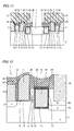
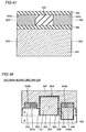
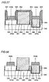
In the drawings:
Embodiments of the present invention are now
described with reference to the drawings.
(First Embodiment)
The structure of a memory cell 1 according to a first
embodiment of the present invention is now described with
reference to Fig. 1.
In the memory cell 1 according to the first
embodiment, an n-type source region 3 and an n-type drain
region 4 are formed on the surface of a p-type single-crystalline
silicon substrate 2 at a prescribed space. A
first gate insulator film 6 of a silicon oxide film, a
control gate electrode 7 of a doped polysilicon film, a
first tunnel insulator film 8 of a silicon oxide film, an
n-type impurity region 9, a second tunnel insulator film
10 of a silicon oxide film, a floating gate electrode 11
of a doped polysilicon film and a third insulator film 12
of a silicon oxide film are formed in this order on a
channel region 5 located between the source region 3 and
the drain region 4 on the surface of the substrate 2. The
second tunnel insulator film 10 and a second gate
insulator film 13 of a silicon oxide film isolate the
floating gate electrode 11 and the channel region 5 from
each other.
The floating gate electrode 11 is embedded in a
trench formed in the p-type single-crystalline silicon
substrate 2, and formed on the side walls of the drain
region 4 through the third insulator film 12.
A source electrode 14 of a doped polysilicon film is
connected to the source region 3. A fourth insulator film
15 of a silicon oxide film isolates the source electrode
14 and the control gate electrode 7 from each other.
The thicknesses of the aforementioned members are set
as follows:
The area of the third insulator film 12 located
between the drain region 4 and the floating gate electrode
11 is larger than that of the second tunnel insulator film
10 located between the n-type impurity region 9 and the
floating gate electrode 11. In the memory cell 1 according
to this embodiment, therefore, the electrostatic
capacitance between the drain region 4 and the floating
gate electrode 11 is larger than that between the n-type
impurity region 9 and the floating gate electrode 11. Thus,
the coupling ratio between the n-type impurity region 9
and the floating gate electrode 11 exceeds that between
the drain region 4 and the floating gate electrode 11.
Consequently, the potential of the drain region 4 is
readily transmitted to the floating gate electrode 11.
Fig. 2 illustrates the overall structure of a
nonvolatile semiconductor memory 50 employing the memory
cell 1.
As shown in Fig. 2, a memory cell array 51 is formed
by arranging a plurality of memory cells 1 in the form of
a matrix (Fig. 2 shows only four memory cells 1, in order
to simplify the illustration).
In the memory cells 1 arranged in a row direction,
the control gate electrodes 7 are connected to common word
lines WL1 to WLn.
In the memory cells 1 arranged in a column direction,
the drain regions 4 are connected to common bit lines BL1
to BLn, and the source electrodes 14 are connected to a
common source line SL.
The word lines WL1 to WLn are connected to a row
decoder 52, and the bit lines BL1 to BLn are connected to a
column decoder 53.
Externally specified row and column addresses are
input in an address pin 54. The address pin 54 transfers
the row and column addresses to an address latch 55. In
the row and column addresses latched in the address latch
55, the row address is transferred to the row decoder 52
through an address buffer 56, and the column address is
transferred to the column decoder 53 through the address
buffer 56.
The row decoder 52 selects a word line corresponding
to the row address latched in the address latch 55 from
the word lines WL1 to WLn and controls the potentials of
the word lines WL1 to WLn in correspondence to respective
operation modes described later on the basis of a signal
from a gate voltage control circuit 57.
The column decoder 53 selects a bit line
corresponding to the column address latched in the address
latch 55 from the bit lines BL1 to BLn and controls the
potentials of the bit lines BL1 to BLn in correspondence to
the respective operation modes described later in response
to a signal from a drain voltage control circuit 58.
Externally specified data is input in a data pin 59.
The data pin 59 transfers the data to the column decoder
53 through an input buffer 60. The column decoder 53
controls the potentials of the bit lines BL1 to BLn in
correspondence to the data as described later.
Data read from an arbitrary memory cell 1 is
transferred from the bit lines BL1 to BLn to a sense
amplifier group 61 through the column decoder 53. The
sense amplifier group 61 is formed by current sense
amplifiers. The data determined in the sense amplifier
group 61 is output from an output buffer 62 through the
data pin 59.
A source voltage control circuit 63 controls the
potential of the source line SL in correspondence to the
operation modes described later.
A control core circuit 54 controls operations of the
aforementioned circuits 52 to 63.
Respective operations (write, erase and read
operations) of the memory cell 1 having the aforementioned
structure are now described. A source voltage Vs is
applied to the source region 3 (the source electrode 14)
through the source line SL. A drain voltage Vd is applied
to the drain region 4 through the bit lines BL1 to BLn. A
control gate voltage Vcg is applied to the control gate
electrode 7 through the word lines WL1 to WLn. A substrate
voltage Vsub is applied to the substrate 2.
(Write Operation)
Before performing the write operation, the floating
gate electrode 11 is in an erased state (where electrons
are extracted), and the floating gate electrode 11 in the
erased state keeps a potential of about 2 V in the first
embodiment. In the first embodiment, it is assumed that
the threshold voltages Vt of transistors having the
floating gate electrode 11 and the control gate electrode
7 as gates respectively are 0.5 V.
In the write operation, the source voltage Vs is set
to 0 V, the drain voltage Vd is set to 3 V, the control
gate voltage Vcg is set to -3 V, and the substrate voltage
(well voltage when the memory cell 1 is formed in a p-type
well formed in the silicon substrate 2: hereinafter
referred to as "well voltage") Vsub is set to 0 V as the
operating voltages of the memory cell 1.
The drain region 4 and the floating gate electrode 11
are strongly electrostatically coupled with each other as
described above, and hence about 2/3 of the drain voltage
(3 V) is added to the potential (about 2 V) in the erased
state of the floating gate electrode 11, so that the
potential of the floating gate electrode 11 consequently
increases to about 4 V. Thus, the transistor having the
floating gate electrode 11 as the gate is turned on and
the potential of the n-type impurity region 9 is
substantially equalized with that of the drain region 4.
In other words, the potential of the n-type impurity
region 9 reaches 3 V (voltage level-shifted from the
potential of the floating gate electrode 11 by the
aforementioned threshold voltage Vt with an upper limit of
the drain voltage Vd) and a high electric field is
generated between the n-type impurity region 9 and the
control gate electrode 7. Consequently, a Fowler-Nordheim
tunnel current (hereinafter referred to as an FN tunnel
current) flows and electrons move from the control gate
electrode 7 to the n-type impurity region 9. Electrons
permeating through (tunneling) the barrier of the first
tunnel insulator film 8 located between the control gate
electrode 7 and the n-type impurity region 9 are
accelerated by the high electric field generated between
the n-type impurity region 9 and the control gate
electrode 7, and injected into the floating gate electrode
11 through the second tunnel insulator film 10.
Consequently, the floating gate electrode 11 stores the
electrons for writing data.
The electrons require energy of 3.2 eV for passing
through the barrier of the second tunnel insulator film 10
of a silicon oxide film, and potential difference
necessary for acquiring the energy is 3.2 V. Therefore,
the aforementioned operating voltages in writing are so
set as to cause potential difference of at least 3.2 V
between the control gate electrode 7 and the n-type
impurity region 9 and between the control gate electrode 7
and the floating gate electrode 11.
When setting the drain voltage Vd to 3 V and the
control gate voltage Vcg to -3V, the voltage of the
floating gate electrode 11 reaches about 4 V and the
potential of the n-type impurity region 9 reaches 3 V due
to the electrostatic coupling between the drain region 4
and the floating gate electrode 11, as hereinabove
described. Therefore, potential difference of 6 V is
initially caused between the control gate electrode 7 and
the n-type impurity region 9, and potential difference of
about 7 V is initially caused between the control gate
electrode 7 and the floating gate electrode 11.
When the energy of the electrons is about 3.2 eV, the
mean free path (the mean value of the moving distances of
the electrons) is about 30 to 40 nm. The width of the n-type
impurity region 9 is set to 30 nm, which is smaller
than the mean free path. Therefore, the electrons
permeating through the barrier of the first tunnel
insulator film 8 located between the control gate
electrode 7 and the n-type impurity region 9 are
accelerated to at least 3.2 eV in a short distance not
more than the mean free path (= about 30 to 40 nm).
Therefore, almost all electrons permeating through
the barrier of the first tunnel insulator film 8 acquire
energy for passing through the barrier (= 3.2 eV) of the
second tunnel insulator film 10 and turn into hot
electrons, which are injected into the floating gate
electrode 11 in an extremely high probability without
remaining in the n-type impurity region 9.
The energy of the electrons and the probability of
passing through the barrier of the first insulator film 8
can be adjusted by the source voltage Vs, the drain
voltage Vd and the control gate voltage Vcg. Therefore,
the hot electrons can be injected into the floating gate
electrode 11 when acquiring energy slightly exceeding the
barrier of the second tunnel insulator film 10.
As hereinabove described, the potential difference of
at least 3.2 V is caused between the control gate
electrode 7 and the n-type impurity region 9 and between
the control gate electrode 7 and the floating gate
electrode 11 in the initial stage of the write operation,
for continuously performing writing (injecting electrons
into the floating gate electrode 11). The electrons are
continuously injected into the floating gate electrode 11
with progress of the write operation, and hence the
potential of the floating gate electrode 11 gradually
lowers from 4 V. As hereinabove described, the potential
of the n-type impurity region 9 reaches a value level-shifted
from the potential of the floating gate electrode
11 by the aforementioned threshold voltage Vt with the
upper limit of the drain voltage Vd. Therefore, the
potential of the n-type impurity region 9 also gradually
lowers along with reduction of the potential of the
floating gate electrode 11, and the potential difference
between the control gate electrode 7 and the n-type
impurity region 9 finally reaches a value less than 3.2 V.
Thus, the electrons contained in the control gate
electrode 7 cannot permeate through the barrier of the
second tunnel insulator film 10 even if the electrons
contained in the control gate electrode 7 can permeate
through the barrier of the first tunnel insulator film 8.
Thereby, the write operation is not further performed.
According to this embodiment, the write operation is
automatically terminated by potential change of the
floating gate electrode 11, whereby no circuit is
separately required for detecting termination of the write
operation. Thus, simplification of the structure in a
peripheral circuit, reduction of the area and reduction of
power consumption can be implemented. Particularly in this
embodiment, the write operation is not terminated in a
constant write time but automatically terminated by the
potential change of the floating gate electrode 11,
whereby dispersion of the write levels can be effectively
prevented between the memory cells 1. Consequently, the
write levels of the memory cells 1 can be substantially
uniformalized.
(Erase Operation)
In the erase operation, the source voltage Vs is set
to 8 V, the drain voltage Vd is set to 0 V, the control
gate voltage Vcg is set to 9 V and the substrate voltage
(well voltage) Vsub is set to 0 V as the operating
voltages of the memory cell 1. In this case, the drain
region 4 and the floating gate electrode 11 are strongly
electrostatically coupled with each other and hence the
potential of the floating gate electrode 11 substantially
reaches 0 V.
On the other hand, the potential of the control gate
electrode 7 is 9 V and hence the transistor having the
control gate electrode 7 as the gate is turned on. Thus,
the potential of the n-type impurity region 9 is
substantially equalized with that of the source region 3.
In other words, the potential of the n-type impurity
region 9 reaches 8 V (voltage level-shifted from the
potential of the control gate electrode 7 by the
aforementioned threshold voltage Vt with an upper limit of
the source voltage Vs). Thus, a high electric field of
about 10 MV is generated in the second tunnel insulator
film 10 located between the n-type impurity region 9 and
the floating gate electrode 11. Consequently, an FN tunnel
current flows and electrons are extracted from the
floating gate electrode 11 to the n-type impurity region 9,
for erasing data.
(Read Operation)
In the read operation, the source voltage Vs is set
to 0 V, the drain voltage Vd is set to 3 V, the control
gate voltage Vcg is set to 3 V and the substrate voltage
(well voltage) Vsub is set to 0 V as the operating
voltages of the memory cell 1.
When the floating gate electrode 11 stores no
electrons (erased state), the floating gate electrode 11
is positively charged (the floating gate electrode 11 has
a potential of 2 V in the first embodiment) and hence the
channel region 5 located under the floating gate electrode
11 enters an ON state. When the floating gate electrode 11
stores electrons (write state), on the other hand, the
floating gate electrode 11 is negatively charged and hence
the channel region 5 located under the floating gate
electrode 11 enters an OFF state.
When the channel region 5 is in an ON state, a
current more readily flows between the source region 3 and
the drain electrode 4 as compared with an OFF state.
Therefore, whether or not the floating gate electrode 11
stores electrons can be determined by detecting the
current (cell current) flowing between the source region 3
and the drain electrode 4. Thus, data stored in the memory
cell 1 can be read.
A similar read operation can be performed also when
reversing the relation between the potentials of the
source voltage Vs and the drain voltage Vd.
According to the first embodiment, the following
functions/effects can be attained:
A method of fabricating the memory cell 1 according
to the first embodiment is now described with reference to
Figs. 3 to 11.
Step 1 (see Fig. 3): Field isolation films 20 of
silicon oxide films are formed on the p-type single-crystalline
silicon substrate 2 by trench isolation or a
LOCOS method. Then, ions for threshold voltage adjustment
are implanted into the surface of the substrate 2. Then,
silicon oxide films 21 are formed on the surface of the
substrate 2 and thereafter worked into the form of
transversely arranged stripes through photolithography and
etching. The p-type single-crystalline silicon substrate 2
corresponds to the "first layer" in the present invention.
The subsequent steps are described with reference to
figures corresponding to a section taken along the line
100-100 in Fig. 3.
Step 2 (see Fig. 4): A silicon nitride film 22 is
formed on the overall surface of the substrate 2 and
thereafter entirely anisotropically etched back, to be
embedded between the silicon oxide films 21.
Every other silicon oxide film 21 is masked with a
resist film 23 for thereafter removing the silicon oxide
films 21 not covered with the resist film 23. Further, the
field isolation film 20 not covered with the resist film
23 and the silicon nitride films 22 are dug down by
overetching.
Thereafter etching gas is switched for digging down
parts of the substrate 2 not covered with the resist film
23 and the silicon nitride films 22 and forming trenches
24 in these portions.
Step 4 (see Fig. 6): The resist film 23 is removed
for thereafter forming thermal oxide films of about 3 nm
in thickness in the trenches 24 by thermal oxidation. In
each thermal oxide film, the portion formed on the bottom
of the trench 24 defines the first gate insulator film 6
and the portion formed on the side wall of the trench 24
defines the first tunnel insulator film 8. The first
tunnel insulator film 8 corresponds to the "first
insulator film" in the present invention.
Step 5 (see Fig. 7): A doped polysilicon film doped
with an n-type impurity such as phosphorus is formed on
the overall surface of the substrate 2 including the
trenches 24 and thereafter entirely anisotropically etched
back for forming the control gate electrodes 7 of side
wall spacers over the trenches 24 and the silicon nitride
films 22. Thus, the control gate electrodes 7 can be
formed in a self-aligned manner with respect to the
silicon nitride films 22. Therefore, the control gate
electrodes 7 can be formed with no problem of misalignment
of a mask in a mask process.
The gate length of the control gate electrodes 7,
which can be controlled by the thickness of the doped
polysilicon film, can be reduced below the minimum limit
size (minimum exposure size) in the mask process and more
precisely controlled than the mask process. Consequently,
the control gate electrodes 7 can be further refined and
prevented from dispersion of the gate length. Each control
gate electrode 7 corresponds to the "first gate electrode"
in the present invention.
The doped polysilicon film can be formed by any of
the following methods:
Further, phosphorus ions are implanted into the
bottom portions of the trenches 24 through the control
gate electrodes 7 serving as masks and thereafter heat
treatment is performed for forming the source regions 3.
Thereafter a silicon oxide film is formed on the overall
surface of the substrate 2 including the trenches 24. The
overall surface of the silicon oxide film is
anisotropically etched back thereby forming the fourth
insulator films 15 of side wall spacers of 30 nm in width
on the side walls of the control gate electrodes 7. Each
source region 3 corresponds to the "first region" in the
present invention.
Step 6 (see Fig. 8): A doped polysilicon film doped
with an n-type impurity such as phosphorus is formed on
the overall surface of the substrate 2 including the
trenches 24. The overall surface of the doped polysilicon
film is anisotropically etched back thereby forming the
source electrodes 14 connected with the source regions 3
in the trenches 24. Thus, the source electrodes 14 can be
formed in a self-aligned manner in the regions enclosed
with the control gate electrodes 7 formed in a self-aligned
manner. Therefore, the source electrodes 14 can be
formed with no problem of misalignment of a mask in a mask
process. Each source electrode 14 corresponds to the
"wire" of the present invention. The doped polysilicon
film is formed by any of the methods described above with
reference to the step 5.
Then, thermal oxide films 25 of 30 to 50 nm in
thickness are formed on the upper surfaces of the control
gate electrodes 7 and the source electrodes 14 by thermal
oxidation. The thermal oxide films 25 and the fourth
insulator films 15 electrically insulate the control gate
electrodes 7 and the source electrodes 14 from each other.
Step 7 (see Fig. 9): The silicon nitride films 22 are
removed and thereafter another silicon nitride film is
formed on the overall surface of the substrate 2. The
overall surface of the silicon nitride film is
anisotropically etched back thereby forming side wall
spacers 26 on the side walls of the silicon oxide film 21
and the control gate electrodes 7.
Further, phosphorus ions are implanted into the
exposed portions of the substrate 2 through the side wall
spacers 26 serving as masks and thereafter heat treatment
is performed thereby forming n-type impurity regions 27.
Step 8 (see Fig. 10): The substrate 2 (the n-type
impurity regions 27) is etched through the side wall
spacers 26, the thermal oxide films 25 and the field
isolation films 20 serving as masks thereby forming
trenches 28 of 200 nm in depth. Each trench 28 divides
each n-type impurity region 27 into two portions. Thus,
the portion of the n-type impurity region 27 located
between each trench 28 and each control gate electrode 7
serves as the n-type impurity region 9. Therefore, the n-type
impurity regions 9 can be formed in a self-aligned
manner with no misalignment of masks in a mask process by
forming the side wall spacers 26 on the side walls of the
control gate electrodes 7 and thereafter etching the
substrate 2 through the side wall spacers 26.
Further, the n-type impurity regions 9 can be formed
with a small width below the limit minimum size in the
mask process by controlling the thickness of the silicon
nitride film for forming the side wall spacers 26. In
addition, the width of the side wall spacers 26 can be
precisely controlled by controlling the thickness of the
silicon nitride film for forming the side wall spacers 26,
whereby the width of the n-type impurity regions 9 formed
through the side wall spacers 26 can also be precisely
controlled.
Thus, the n-type impurity regions 9 can be further
refined and prevented from dispersion in width. Each n-type
impurity region 9 corresponds to the "third region"
in the present invention.
The width (the distance between the trench 28 and the
first tunnel insulator film 8) of each n-type impurity
region 9 is 30 nm. The range of the width of the n-type
impurity regions 9 is properly not more than 50 nm,
desirably not more than 30 to 40 nm below the mean free
path of carriers, and more desirably 20 to 30 nm.
If the width of the n-type impurity regions 9 exceeds
50 nm, the write efficiency and the erase efficiency tend
to lower.
Then, thermal oxide films of about 8 nm in thickness
are formed in the trenches 28 by thermal oxidation. In
these thermal oxide films, portions formed on the bottoms
of the trenches 28 define the second gate insulator films
13, portions formed on the side walls of the trenches 28
closer to the n-type impurity regions 9 define the second
tunnel insulator films 10, and portions formed on the side
walls of the trenches 28 closer to the drain regions 4
define the third insulator films 12. Each second tunnel
insulator film 10 corresponds to the "second insulator
film" in the present invention.
A doped polysilicon film doped with an n-type
impurity such as phosphorus is formed on the overall
surface of the substrate 2 including the trenches 28 and
thereafter entirely anisotropically etched back. Further,
the doped polysilicon film is etched toward the surface of
the substrate 2 through the side wall spacers 26, the
thermal oxide films 25 and the field isolation films 20
serving as masks, thereby embedding/forming the floating
gate electrodes 11 in the trenches 28. Each floating gate
electrode 11 corresponds to the "second gate electrode" in
the present invention.
The doped polysilicon film is formed by any of the
methods described above with reference to the step 5.
Thereafter thermal oxide films 29 are formed on the
upper surfaces of the floating gate electrodes 11 by
thermal oxidation. In this stage, the floating gate
electrodes 11 of the respective memory cells 1 are formed
independently of each other through the field isolation
films 20.
Step 9 (see Fig. 11): A silicon nitride film 30 is
formed on the overall surface and thereafter etched back.
Regions excluding the silicon oxide film 21 are covered
with a resist film 31 and thereafter the silicon oxide
film 21 is removed by etching for exposing the substrate 2.
Phosphorus ions are implanted into the exposed portion of
the substrate 2 and thereafter heat treatment is performed
for forming the n-type drain region 4. At this time, the
n-type impurity regions 27 are integrated with the drain
region 4. Thus, the floating gate electrodes 11 are formed
on the side walls of the drain region 4 through the third
insulator films 12. The n-type drain region 4 corresponds
to the "second region" in the present invention.
Thus, the memory cells 1 are completed.
Thereafter an interlayer isolation film (not shown)
is formed on the memory cells 1. The word lines WL0 to WLn
connecting the control gate electrodes 7, the bit lines BL0
to BLn connecting the drain regions 4 and the source line
SL connecting the source electrodes 14 in common are
formed thereby forming the memory cell array 50.
(Second Embodiment)
A second embodiment of the present invention is now
described. In the second embodiment, data of four values
("00", "01", "10" and "11") are stored in the structure of
the memory cell 1 according to the first embodiment.
Therefore, the second embodiment is different from the
first embodiment only in operating voltages in writing,
and the remaining structure of the second embodiment is
identical to that of the first embodiment.
In a write operation, operating voltages of the
memory cell 1 are set to values shown in Table 1 for the
data "01", "10" and "11" respectively. Data "00" is for an
erased state.
| Data | Source Voltage Vs | Control Gate Voltage Vcg | Drain Voltage Vd |
| 01 | 0 | -3 | 3 |
| 10 | 0 | -3 | 4 |
| 11 | 0 | -3 | 5 |
| (substrate voltage Vsub : 0 V) |
The drain voltage Vd varies with the types of the
data. In the write operation, writing is terminated when
the potential difference between the control gate
electrode 7 and the n-type impurity region 9 is less than
3.2 V, as described above. On the other hand, the initial
voltage of the n-type impurity region 9 is increased in
proportion to the drain voltage Vd and hence the time for
reducing the potential difference between the control gate
electrode 7 and the n-type impurity region 9 to less than
3.2 V is so increased that a large quantity of electrons
are injected into the floating gate electrode 11. In other
words, the quantity of electrons stored in the floating
gate electrode 11 can be varied by changing the drain
voltage Vd. Multivalued (four-valued) data can be written
by associating the written data with the storage
quantities.
In a read operation, a current (cell current) hardly
flows between the source region 3 and the drain electrode
4 and the value thereof is reduced as the quantity of
electrons stored in the floating gate electrode 11 is
increased. Thus, data stored in the memory cell 1 can be
read by associating the current values and the four-valued
data.
(Third Embodiment)
Referring to Fig. 12, a drain region is formed in a
diode structure in a memory cell 1 according to a third
embodiment of the present invention having a structure
similar to that of the memory cell 1 according to the
first embodiment shown in Fig. 1. The remaining structure
of the memory cell 1 according to the third embodiment is
identical to that of the first embodiment.
According to the third embodiment, an n-type drain
region 4a, a p-type drain region 4b and a drain region 4c
of a p-type polysilicon film form the drain region of the
diode structure, as shown in Fig. 12. The n-type drain
region 4a is formed on the overall region between a p-type
single-crystalline silicon substrate 2 and the p-type
drain region 4b. The p-type drain region 4b and the drain
region 4c of a p-type polysilicon film define the "fourth
region" of the present invention. The drain region 4c of
the p-type polysilicon film is embedded in the p-type
drain region 4b. The n-type drain region 4a and the p-type
drain region 4b are capacitively coupled with a floating
gate electrode 11 through a third insulator film 12.
Write and read operations of the third embodiment are
identical to those of the first embodiment. As to
operating voltages in an erase operation of the third
embodiment, however, a negative voltage is applied to the
drain region dissimilarly to the first embodiment.
More specifically, a source voltage Vs is set to 5.5
V, a drain voltage Vd is set to -4 V, a control gate
voltage Vcg is set to 5.5 V and a substrate voltage (well
voltage) Vsub is set to 0 V as the operating voltages of
the memory cell 1 in the erase operation. In this case,
the drain region is strongly electrostatically coupled
with the floating gate electrode 11 and hence the
potential of the floating gate electrode 11 substantially
reaches -3 V.
On the other hand, the potential of a control gate
electrode 7 is 5.5 V and hence a transistor having the
control gate electrode 7 as the gate enters an ON state.
Thus, the potential of an n-type impurity region 9 is
substantially equalized with that of a source region 3. In
other words, the potential of the n-type impurity region 9
reaches 5 V (voltage level-shifted from the potential of
the control gate electrode 7 by a threshold voltage Vt
with the upper limit of the source voltage Vs). Thus, a
high electric field of about 10 MV is generated in a
second tunnel insulator film 10 located between the n-type
impurity region 9 and the floating gate electrode 11.
Consequently, an FN tunnel current flows and electrons are
extracted from the floating gate electrode 11 into the n-type
impurity region 9 for erasing data.
According to the third embodiment, the following
functions/effects can be attained in addition to the
aforementioned functions/effects of the first and second
embodiments:
A method of fabricating the memory cell 1 according
to the third embodiment is now described with reference to
Figs. 13 and 14. In the fabrication process for the memory
cell 1 according to the third embodiment, the structure
shown in Fig. 10 is formed through a process similar to
the fabrication process according to the first embodiment
shown in Figs. 2 to 10, followed by subsequent steps 10
and 11.
Step 10 (see Fig. 13): A silicon nitride film 30 is
formed on the overall surface and thereafter etched back.
Regions excluding a silicon oxide film 21 (see Fig. 10)
are covered with a resist film 31 and thereafter the
silicon oxide film 21 is removed by etching for exposing
the substrate 2. The substrate 2 is further dug down.
Phosphorus ions are implanted into the exposed part of the
substrate 2. Thus, the n-type drain region 4a is formed.
Step 11 (see Fig. 14): A polysilicon film is
deposited on the overall surface, and thereafter a p-type
impurity is ion-implanted. Heat treatment is performed and
thereafter the polysilicon film is etched back. The n-type
drain region 4a is activated by the heat treatment while
the p-type impurity diffuses from the polysilicon film for
forming the p-type drain region 4b. Further, the p-type
drain region 4a of a p-type polysilicon film is formed by
etching back the polysilicon film.
Thus, the drain region including the n-type drain
region 4a, the p-type drain region 4b and the drain region
4c of the p-type polysilicon film is formed. n-type
impurity regions 27 (see Fig. 10) are replaced with p-type
layers since the quantity of the p-type impurity diffusing
later is larger, and integrated with the p-type drain
region 4b. The n-type drain region 4a corresponds to the
"second region" in the present invention, and the p- type
drain regions 4b and 4c correspond to the "fourth region"
in the present invention.
The memory cell 1 is completed in the aforementioned
manner.
Thereafter an interlayer isolation film (not shown)
is formed on each memory cell 1, similarly to the first
embodiment. Word lines WL0 to WLn connecting each control
gate electrode 7, bit lines BL0 to BLn connecting each
drain region and a source line SL connecting each source
electrode 14 in common are formed for forming a memory
cell array 50.
(Fourth Embodiment)
With reference to Fig. 15, the structure of a memory
cell 101 according to a fourth embodiment of the present
invention is now described.
In the memory cell 101 according to the fourth
embodiment, an n-type source region 103 and an n-type
drain region 104 are formed on the surface of a p-type
single-crystalline silicon substrate 102 at a prescribed
space to hold a channel region 105 therebetween. A
floating gate electrode 111 of an n-type polysilicon film
is formed on the channel region 105 and a part of the
drain region 104 through a second gate insulator film 112a
of a silicon oxide film and a third insulator film 112b.
An inter-gate 109 of an n-type single-crystalline
silicon film is formed on the side surface and the upper
surface of the floating gate electrode 111 through a
second tunnel insulator film 110. The bottom portion of
the inter-gate 109 is in contact with the surface of the
p-type single-crystalline silicon substrate 102 through an
opening 115. An n-type diffusion layer 114 is formed under
the contact surfaces of the inter-gate 109 and the p-type
single-crystalline silicon substrate 102.
A control gate electrode 107 of an n-type polysilicon
film is formed on the side surface and the upper surface
of the inter-gate 109 through a first tunnel insulator
film 108. The bottom portion of the control gate electrode
107 is formed on the channel region 105 through a first
gate insulator film 106 of a silicon oxide film.
The thicknesses of the aforementioned members in the
fourth embodiment are set as follows:
The area of the third insulator film 112b located
between the drain region 104 and the floating gate
electrode 111 is larger than that of the second tunnel
insulator film 110 located between the inter-gate 109 and
the floating gate electrode 111 while the thickness of the
third insulator film 112b is smaller than that of the
second tunnel insulator film 110.
In the memory cell 101 according to this embodiment,
therefore, the electrostatic capacitance between the drain
region 104 and the floating gate electrode 111 is larger
than that between the inter-gate 109 and the floating gate
electrode 111. Thus, the coupling ratio between the inter-gate
109 and the floating gate electrode 111 is larger
than that between the drain region 104 and the floating
gate electrode 111. Consequently, the potential of the
drain region 104 is readily transmitted to the floating
gate electrode 111.
Respective operations (write, erase and read
operations) of the memory cell 101 according to the fourth
embodiment are similar to those in the first embodiment.
According to the fourth embodiment, the following
functions/effects can be attained in addition to those
according to the first to third embodiments:
A method of fabricating the memory cell 101 according
to the fourth embodiment is now described with reference
to Figs. 16 to 20.
Step 12 (see Fig. 16): A silicon oxide film 112 is
formed on the p-type single-crystalline silicon substrate
102 in a thickness of about 8 to 10 nm by thermal
oxidation. A doped polysilicon film doped with an n-type
impurity is formed on the silicon oxide film 112 in a
thickness of about 200 nm by LPCVD at a deposition
temperature of about 620°C. Another silicon oxide film is
further deposited on the doped polysilicon film. The
silicon oxide film and the doped polysilicon film are
patterned by photolithography and dry etching, thereby
forming the floating gate electrode 111 of the n-type
doped polysilicon film and a silicon oxide film 121
located thereon. The p-type single-crystalline silicon
substrate 102 corresponds to the "first layer" of the
present invention, and the floating gate electrode 111
corresponds to the "second gate electrode" of the present
invention.
The doped polysilicon film may be formed by any of
the following methods:
Step 13 (see Fig. 17): A resist film 122 is formed to
cover a source forming region. The resist film 122 is
employed as a mask for implanting phosphorus ions into the
surface of the p-type single-crystalline silicon substrate
102 under conditions of about 50 key and 1E15/cm2 thereby
forming the drain region 104. This drain region 104 is so
formed as to extend substantially toward the center of the
lower portion of the floating gate electrode 111, in order
to increase the area of the portion overlapping with the
floating gate electrode 111. In the silicon oxide film 112,
the part held between the floating gate electrode 111 and
the p-type single-crystalline silicon substrate 102
defines the second gate insulator film 112a, and the part
held between the floating gate electrode 111 and the drain
region 104 defines the third insulator film 112b. The
drain region 104 corresponds to the "second region" of the
present invention.
Step 14 (see Fig. 18): The resist film 122 is removed
and thereafter the silicon oxide film 121 is removed from
the floating gate electrode 111. Further, parts of the
silicon oxide film 112 other than those defining the
second gate insulator film 112a and the third insulator
film 112b are removed. A silicon oxide film having a
thickness of about 16 to 20 nm is formed on the upper
surface and the side surface of the floating gate
electrode 111 and the surface of the p-type single-crystalline
silicon substrate 102 by thermal oxidation. In
this silicon oxide film, the part formed on the side
surface of the floating gate electrode 111 to be formed
with the inter-gate 109 and the upper surface of this
portion defines the second tunnel insulator film 110, and
the part located between the p-type single-crystalline
silicon substrate 102 and the portion to be formed with
the control gate electrode 107 defines the first gate
insulator film 106. The second tunnel insulator film 110
corresponds to the "second insulator film" in the present
invention.
Step 15 (see Fig. 19): The opening 115 is formed by
lithography and dry etching. An amorphous silicon film
109a is formed on the overall surface in a thickness of
about 20 to 40 nm by LPCVD at a deposition temperature of
about 560°C. Phosphorus ions are implanted into the
amorphous silicon film 109a under conditions of 3 keV and
1E14/cm2.
Step 16 (see Fig. 20): The amorphous silicon film
109a is patterned thereby forming the inter-gate 109. Heat
treatment is performed at a temperature of about 600°C for
about two hours, thereby single-crystallizing the inter-gate
109 while forming the n-type diffusion layer 114 on
the p-type single-crystalline silicon substrate 102. The
inter-gate 109 corresponds to the "third region" or the
"semiconductor region" of the present invention.
Thereafter the first insulator film 108 having a
thickness of about 3 to 4 nm is formed on the side surface
and the upper surface of the inter-gate 109 of a single-crystalline
silicon film by thermal oxidation. The first
tunnel insulator film 108 corresponds to the "first
insulator film" in the present invention. A doped
polysilicon film or a WSi film is formed to cover the
overall surface.
The width of the inter-gate 109 (the distance between
the first and second tunnel insulator films 108 and 110)
is 30 nm. The width of the inter-gate 109 is properly in
the range of not more than 50 nm, preferably not more than
30 to 40 nm, i.e., not more than the mean free path of
carriers, and more preferably in the range of 20 to 30 nm.
If the width of the inter-gate 109 exceeds 50 nm, write
efficiency and erase efficiency tend to lower.
Thereafter the doped polysilicon film or the WSi film
is patterned thereby forming the control gate electrode
107, as shown in Fig. 15. A resist film (not shown) is
formed to cover the drain region 104 and thereafter
employed as a mask for ion-implanting an n-type impurity
such as phosphorus into the p-type single-crystalline
silicon substrate 102, thereby forming the source region
103. The control gate electrode 107 corresponds to the
"first gate electrode" in the present invention, and the
source region 103 corresponds to the "first region" in the
present invention.
The memory cell 101 according to the fourth
embodiment is thus completed.
Thereafter an interlayer isolation film (not shown)
is formed on each memory cell 101. Word lines WL0 to WLn
connecting each control gate electrode 107, bit lines BL0
to BLn connecting each drain region 104 and a source line
SL connecting each source region 103 in common are formed
for forming a memory cell array 50.
(Fifth Embodiment)
In a memory cell 171 according to a fifth embodiment
of the present invention, two side wall films form an
inter-gate in a self-aligned manner while two side wall
films form part of a drain region in a self-aligned manner
as shown in Fig. 21, dissimilarly to the fourth embodiment.
The remaining basic structure of the memory cell 171 is
substantially similar to that of the memory cell 101
according to the fourth embodiment. The fifth embodiment
is now described.
In the memory cell 171 according to the fifth
embodiment, an n-type source region 173 and an n-type
drain region 174 are formed on the surface of a p-type
single-crystalline silicon substrate 172 at a prescribed
space to hold a channel region 175 therebetween. On the
channel region 175 and part of the drain region 174, a
floating gate electrode 182 of a doped polysilicon film is
formed through a second gate insulator film 183a of a
silicon oxide film and a third insulator film 183b. An
inter-gate 181a of an n-type polysilicon film is formed on
the side surface of the floating gate electrode 182
through a second tunnel insulator film 184a.
This inter-gate 181a is formed by a side wall film
179a of an n-type polysilicon film and a side wall film
180a of an n-type polysilicon film. The bottom portion of
the side wall film 180a is in contact with the surface of
the p-type single-crystalline silicon substrate 172.
On the drain region 174, a drain region 181b is
formed by side wall films 179b and 180b of polysilicon
films. The side wall film 180b and the drain region 174
are electrically connected with each other. A third
insulator film 184b is formed between the drain region
181b and the floating gate electrode 182. In other words,
the third insulator films 183b and 184b are formed between
the drain regions 174 and 181b and the floating gate
electrode 182.
A control gate electrode 177 of an n-type polysilicon
film is formed on the side surface of the inter-gate 181a
through a first tunnel insulator film 178. The bottom
portion of the control gate electrode 177 is formed on the
channel region 175 through a first gate insulator film
176a of a silicon oxide film.
An interlayer isolation film 191 is formed to cover
the overall surface. A plug electrode 192 is formed in a
contact hole provided in the interlayer isolation film 191.
A bit line 193 connected to the plug electrode 192 is
formed to extend on the interlayer isolation film 191.
Write, erase and read operations of the fifth
embodiment are identical to those of the first embodiment.
According to the fifth embodiment, the following
functions/effects can be attained in addition to those
according to the first to fourth embodiments:
A method of fabricating the memory cell 171 according
to the fifth embodiment is now described with reference to
Figs. 22 to 36.
Step 17 (see Figs. 22 and 23): An element isolation
film 185 is formed on the surface of the p-type single-crystalline
silicon substrate 172 by an STI (shallow
trench isolation) method. The p-type single-crystalline
silicon substrate 172 corresponds to the "first layer" in
the present invention. The element isolation film 185 may
alternatively be formed by another method such as a LOCOS
(local oxidation of silicon) method.
Step 18 (see Fig. 24): A silicon oxide film 183 is
formed on the p-type single-crystalline silicon substrate
172 in a thickness of about 8 to 10 nm by thermal
oxidation. An n-type doped polysilicon film 182 is formed
on the silicon oxide film 183 by LPCVD in a thickness of
about 150 nm. The doped polysilicon film 182 is formed by
any of the methods described with reference to the step 5.
Step 19 (see Fig. 25): A silicon oxide film 190 is
deposited on the doped polysilicon film 182 in a thickness
of about 200 nm.
Step 26 (see Fig. 26): A resist film 194 is
selectively formed on the silicon oxide film 190 by
photolithography, and thereafter employed as a mask for
selectively etching the silicon oxide film 190 and the
doped polysilicon film 182. Thus, the floating gate
electrode 182 of a patterned n-type doped polysilicon film
is formed with the silicon oxide film 190 located thereon.
The floating gate electrode 182 corresponds to the "second
gate electrode" in the present invention.
Step 21 (see Fig. 27): The resist film 194 is removed
and thereafter parts of the silicon oxide film 183 except
that located under the floating gate electrode 182 are
removed by wet etching with hydrofluoric acid. At this
time, the side surfaces of the silicon oxide film 190
located on the floating gate electrode 182 are also
slightly removed. Thereafter the second tunnel insulator
film 184a of a silicon oxide film and the third insulator
film 184b are formed on the side surfaces of the floating
gate electrode 182 in thicknesses of about 10 nm, and the
doped polysilicon film 79 is thereafter formed by LPCVD in
a thickness of about 25 nm. The doped polysilicon film 79
is formed by any of the methods described with reference
to the step 5. The second tunnel insulator film 184a
corresponds to the "second insulator film" of the present
invention.
Step 22 (see Fig. 28): The overall surface of the
doped polysilicon film 79 is etched back by RIE (reactive
ion etching), thereby forming side wall films 179 of doped
polysilicon films on the side surfaces of the floating
gate electrode 182.
Step 23 (see Fig. 29): The silicon oxide film 183 is
etched through the side wall films 179 serving as masks,
thereby selectively removing the silicon oxide film 183.
Thereafter a non-doped polysilicon film 80 is formed by
LPCVD in a thickness of about 25 nm.
Step 24 (see Fig. 30): The overall surface of the
non-doped polysilicon film 80 is etched back by RIE
(reactive ion etching), thereby forming side wall films
180 of non-doped polysilicon films on the side surfaces of
the side wall films 179. An n-type impurity contained in
the side wall films 179 diffuses into the side wall films
180 in a later heat treatment step, thereby supplying the
side wall films 180 with conductivity. Thus, the side wall
films 179 and 180 are integrated with each other.
The side wall films 180 are not formed by doped
polysilicon films for the following reason: When forming
the polysilicon film 80 for defining the side wall films
180 by a doped polysilicon film in the step shown in Fig.
29, the impurity contained in the polysilicon film 80
which is in contact with the surface of the p-type single-crystalline
silicon substrate 172 disadvantageously
diffuses into the surface of the p-type single-crystalline
silicon substrate 172. In the fifth embodiment, therefore,
the non-doped polysilicon film 80 is formed for thereafter
forming the side wall films 180 from the non-doped
polysilicon film 80 and further diffusing the n-type
impurity contained in the side wall films 179 into the
side wall films 180 in the later heat treatment step for
supplying the side wall films 180 with conductivity.
The thicknesses of the side wall films 179 and 180
formed by etching back the polysilicon films 79 and 80
respectively are about 60 % of the thicknesses (25 nm
each) of the deposited polysilicon films 79 and 80.
Therefore, the thicknesses, 15 nm each, of the side wall
films 179 and 180, are about 30 nm in total.
Step 25 (see Figs. 31 and 32): A resist film 195 is
formed on the silicon oxide film 190 to expose ends of the
floating gate electrode 182 along a direction Y, as shown
in Fig. 31. The resist mask 195 is employed as a mask for
selectively removing the side wall films 179 and 180
located on the ends of the floating gate electrode 182
along the direction Y. Thus, the inter-gate 181a formed by
the side wall films 179a and 180a and the drain region
181b formed by the side wall films 179b and 180b are
electrically isolated from each other in a section along a
direction X, as shown in Fig. 32. The inter-gate 181a and
the drain region 181b electrically isolated from each
other are simultaneously formed in the aforementioned
manner. Thereafter a silicon oxide film 176 for defining
the first gate insulator film 176a is formed on the
surface of the p-type single-crystalline silicon substrate
172.
The inter-gate 181a corresponds to the "third region",
the "semiconductor region" or the "first side wall film"
of the present invention. The side wall films 179a and
180a correspond to the "second side wall film" and the
"third side wall film" in the present invention
respectively. The drain region 181b corresponds to the
"second region" or the "fourth side wall film" in the
present invention. Further, the side wall films 179b and
180b correspond to the "fifth side wall film" and the
"sixth side wall film" in the present invention
respectively.
Step 26 (see Fig. 33): After removing the resist film
195, another resist film 196 is formed to cover the source
region side. The resist film 196 is employed as a mask for
implanting As ions, for example, into the surface of the
p-type single-crystalline substrate 172 under conditions
of about 40 keV and 5E15/cm2, thereby forming the n-type
drain region 174. This drain region 174 is so formed as to
extend substantially to the center of the lower portion of
the floating gate electrode 182, in order to increase the
area of the portion overlapping with the floating gate
electrode 182.
In the silicon oxide film 183, the part held between
the floating gate electrode 182 and the p-type single-crystalline
silicon substrate 172 defines the second gate
insulator film 183a, and the part held between the
floating gate electrode 182 and the drain region 174
defines the third insulator film 183b. The drain region
184 corresponds to the "second region" of the present
invention. The third insulator film 183b is employed as an
insulator film located between the drain regions 184 and
181b and the floating gate electrode 182 along with the
aforementioned third insulator film 184b.
Step 27 (see Fig. 34): After removing the resist film
196, a silicon oxide film is formed in a thickness of
about 3 to 4 nm. In this silicon oxide film, the part
located on the side surfaces of the side wall films 179a
and 180a defines the first tunnel insulator film 178. The
first tunnel insulator film 178 forms the "first insulator
film" of the present invention. Thereafter a doped
polysilicon film 77 is formed on the overall surface. This
doped polysilicon film 77 is formed by any of the methods
described with reference to the step 5. After depositing a
non-doped polysilicon film, for example, phosphorus ions
are implanted into the non-doped polysilicon film by about
4E15/cm2 for supplying conductivity, thereby forming the
doped polysilicon film 77.
Step 28 (see Fig. 35): A resist film 197 is formed on
a prescribed region of the doped polysilicon film 77 and
thereafter employed as a mask for etching the doped
polysilicon film 77, thereby forming the control gate
electrode 177. This control gate electrode 177 is formed
on the p-type single-crystalline silicon substrate 172
through the first gate insulator film 176a. The control
gate electrode 177 corresponds to the "first gate
electrode" of the present invention.
Step 29 (see Fig. 36): After removing the resist film
197, another resist film 198 is formed to cover the drain
region 174. The resist film 198 and the control gate
electrode 177 are employed as masks for ion-implanting an
n-type impurity into the p-type single-crystalline silicon
substrate 172, thereby forming the n-type source region
173. The source region 173 corresponds to the "first
region" of the present invention. Thereafter the resist
film 198 is removed.
Thereafter the interlayer isolation film 191 is
formed as shown in Fig. 21, and the bit line 193 (BL0 to
BLn) connecting each drain region 194 is formed through the
plug electrode 192.
The memory cell 171 according to the fifth embodiment
is completed in the aforementioned manner.
(Sixth Embodiment)
The structure of a memory cell 201 according to a
sixth embodiment of the present invention is now described
with reference to Fig. 38.
In the memory cell 201 according to this embodiment,
an n-type source region 203 and an n-type drain region 204
are respectively formed on both side surfaces of a trench
formed in the surface of a p-type single-crystalline
silicon substrate 202. The source region 203 and the drain
region 204 are formed at a prescribed space to hold a
channel region 205 therebetween. In the trench of the p-type
single-crystalline silicon substrate 202, a control
gate electrode 207 of an n-type polysilicon film and a
floating gate electrode 211 of an n-type polysilicon film
are formed at a prescribed space. The control gate
electrode 207 is defined by a first side wall film formed
on the side surface of the source region 203 in a self-aligned
manner through a third insulator film 214. The
control gate electrode 207 is formed on the channel region
205 through a first gate insulator film 206 of a silicon
oxide film.
The floating gate electrode 211 is defined by a
second side wall film formed on the side surface of the
drain region 204 in a self-aligned manner through a fourth
insulator film 212. The floating gate electrode 211 is
formed on the channel region 205 through a second gate
insulator film 213 of a silicon oxide film.
An inter-gate 209 of an n-type polysilicon film is
formed between the control gate electrode 207 and the
floating gate electrode 211. The bottom portion of the
inter-gate 209 is in contact with the surface of the p-type
single-crystalline silicon substrate 207. A first
tunnel insulator film 208 is formed between the inter-gate
209 and the control gate electrode 207. A second tunnel
insulator film 210 is formed between the inter-gate 209
and the floating gate electrode 207. A fifth insulator
film 215 is formed on the upper surface of the inter-gate
209 located between the control gate electrode 207 and the
fifth insulator film 215.
The thicknesses of the aforementioned members are set
as follows:
The area of the fourth insulator film 212 located
between the drain region 204 and the floating gate
electrode 211 is larger than that of the second tunnel
insulator film 210 located between the inter-gate 209 and
the floating gate electrode 211.
In the memory cell 201 according to the sixth
embodiment, therefore, the electrostatic capacitance
between the drain region 204 and the floating gate
electrode 211 is larger than that between the inter-gate
209 and the floating gate electrode 211. Thus, the
coupling ratio between the inter-gate 209 and the floating
gate electrode 211 is larger than that between the drain
region 204 and the floating gate electrode 211.
Consequently, the potential of the drain region 204 is
readily transmitted to the floating gate electrode 211.
Respective operations (write, erase and read
operations) of the memory cell 201 according to the sixth
embodiment having the aforementioned structure are similar
to those in the first embodiment.
According to the sixth embodiment, the following
functions/effects can be attained in addition to those
according to the first to fifth embodiments:
A method of fabricating the memory cell 201 according
to this embodiment is now described with reference to Figs.
39 to 46.
Step 30 (see Fig. 39): Field isolation films 216 of
silicon oxide films are formed on the surface of the p-type
single-crystalline silicon substrate 202 by an STI
(shallow trench isolation) method or a LOCOS (local
oxidation of silicon) method. The p-type single-crystalline
silicon substrate 202 corresponds to the
"first layer" in the present invention.
The following description is made with reference to
sectional views taken along the line 100-100 in Fig. 39.
Step 31 (see Fig. 40): A silicon oxide film 217 is
deposited on the overall surface in a thickness of about
150 nm, and thereafter a resist film 218 is selectively
formed on the silicon oxide film 217 by lithography. The
resist film 218 is employed as a mask for anisotropically
etching the silicon oxide film 217, thereby removing parts
of the silicon oxide film 217 not covered with the resist
film 218.
Step 32 (see Fig. 41): After removing the resist film
218, the silicon oxide film 217 is employed as a mask for
ion-implanting an n-type impurity (31P+, for example) into
the p-type single-crystalline silicon substrate 202 under
conditions of 100 keV and 5.0E15/cm2. Thus, the n-type
source region 203 and the n-type drain region 204 are
formed. The source region 203 corresponds to the "first
region" of the present invention, and the drain region 204
corresponds to the "second region" of the present
invention.
Step 33 (see Fig. 42): A silicon nitride film 219 is
deposited on the overall surface in a thickness of about
150 nm, and thereafter polished by CMP (chemical
mechanical polishing) to expose the silicon oxide film 217
located under the silicon nitride film 219.
Step 34 (see Fig. 43): After removing the silicon
oxide film 217, the silicon nitride film 219 is employed
as a mask for digging down the p-type single-crystalline
silicon substrate 202 by about 150 nm, thereby forming the
trench. The silicon nitride film 219 is removed by wet
etching, and thereafter a thermal oxide film having a
thickness of about 10 nm is formed on the surface of the
p-type single-crystalline silicon substrate 202 and in the
trench. In this thermal oxide film, the part formed on the
side surface of the source region 203 defines the third
insulator film 214, and the part formed on the side
surface of the drain region 204 defines the fourth
insulator film 212.
Step 35 (see Fig. 44): A doped polysilicon film doped
with an n-type impurity such as phosphorus is formed on
the overall surface in a thickness of about 200 nm, and
thereafter the overall surface thereof is anisotropically
etched back thereby simultaneously forming the control
gate electrode 207 and the floating gate electrode 211 of
side wall films. Thus, the control gate electrode 207 and
the floating gate electrode 211 can be formed in a self-aligned
manner with respect to the source region 203 and
the drain region 204 respectively. The control gate
electrode 207 corresponds to the "first gate electrode" of
the present invention, and the floating gate electrode 211
corresponds to the "second gate electrode" of the present
invention.
The doped polysilicon film is formed by any of the
methods described with reference to the step 5.
Step 36 (see Fig. 45): A resist film (not shown) is
formed on the parts of the floating gate electrode 211
other than those located on the field isolation films 216,
and thereafter employed as a mask for anisotropically
etching the floating gate electrode 211. Thus, the parts
of the floating gate electrode 211 located on the field
isolation films 216 are removed for defining the floating
gate electrode 211 independent for each memory cell 201.
Step 37 (see Fig. 46): A thermal oxide film having a
thickness of about 10 nm is formed on the side surfaces of
the control gate electrode 207 and the floating gate
electrode 211 by thermal oxidation. In this thermal oxide
film, the part formed on the side surface of the control
gate electrode 207 defines the first tunnel insulator film
208, and the part formed on the side surface of the
floating gate electrode 211 defines the second tunnel
insulator film 210. The part of the thermal oxide film
formed between the control gate electrode 207 and the
floating gate electrode 211 is removed by etchback. Thus,
the first gate insulator film 206 and the second gate
insulator film 213 are formed.
The first and second tunnel insulator films 208 and
210 are also slightly removed by this etchback so that the
thicknesses thereof are about 8 nm respectively. Further,
the thickness of the first tunnel insulator film 208 is
reduced to about 3 nm by masking the remaining portions
and thereafter etching back the first tunnel insulator
film 208. The first tunnel insulator film 208 corresponds
to the "first insulator film" of the present invention,
and the second tunnel insulator film 210 corresponds to
the "second insulator film" of the present invention.
A doped polysilicon film doped with an n-type
impurity such as phosphorus is deposited on the overall
surface and thereafter embedded in the trench by etchback
or CMP. The doped polysilicon film is formed by any of the
methods described with reference to the step 5. Thus, the
inter-gate 209 of an n-type doped polysilicon film can be
formed in a self-aligned manner with respect to the
control gate electrode 207 and the floating gate electrode
211. The bottom surface of the inter-gate 209 is in
contact with the p-type single-crystalline silicon
substrate 202. The inter-gate 209 corresponds to the
"third region" or the "semiconductor region" of the
present invention.
Thereafter the upper surface of the inter-gate 209 of
a doped polysilicon film is thermally oxidized under
conditions of about 900°C and for about 30 minutes by wet
oxidation, thereby forming the fifth insulator film 215.
The fifth insulator film 215 can reliably isolate the
control gate electrode 207 and the floating gate electrode
211 from the inter-gate 209.
In the step 37, the first and second tunnel insulator
films 208 and 210 are more readily etched back on the
upper portions of the side surfaces of the control gate
electrode 207 and the floating gate electrode 211 of side
wall films than on the lower portions. When the first and
second tunnel insulator films 208 and 210 are etched back,
therefore, the portions located on the upper portions of
the side surfaces of the control gate electrode 207 and
the floating gate electrode 211 may disappear. In this
case, the inter-gate 209 disadvantageously electrically
comes into contact with the control gate electrode 207 and
the floating gate electrode 211.
According to the sixth embodiment, the fifth
insulator film 215 is formed on the upper surface of the
inter-gate 209, so that the inter-gate 209 can be reliably
isolated from the control gate electrode 207 and the
floating gate electrode 211 also when the portions of the
first and second tunnel insulator films 208 and 210
located on the upper portions of the side surfaces of the
control gate electrode 207 and the floating gate electrode
211 disappear.
The mean value of the width of the inter-gate 209
(the distance between the first and second tunnel
insulator films 208 and 210) is about 30 nm. The width of
the inter-gate 209 is properly in the range of not more
than 50 nm, desirably not more than 30 to 40 nm, i.e., not
more than the mean free path of carriers, and more
desirably in the range of 20 to 30 nm. If the width of the
inter-gate 209 exceeds 50 nm, write efficiency and erase
efficiency tend to lower.
The memory cell 201 according to the sixth embodiment
is thus completed.
Thereafter an interlayer isolation film (not shown)
is formed on each memory cell 201. Word lines WL0 to WLn
connecting each control gate electrode 207, bit lines BL0
to BLn connecting each drain region 204 and a source line
SL connecting each source region 203 in common are formed
for forming a memory cell array 50.
(Seventh Embodiment)
A seventh embodiment of the present invention is
different in structure and operating method from the
aforementioned first to sixth embodiments. However, data
writing is performed through an n-type impurity region
(third region), similarly to the first to sixth
embodiments. The seventh embodiment is now described.
According to the seventh embodiment, a source region
343 of an n-type impurity region is formed on a p-type
single-crystalline silicon substrate 342, as shown in Figs.
47 and 48. A drain region 344a of an n-type polysilicon
film is formed at a prescribed space from the source
region 343. The n-type drain region 344a is formed on the
p-type single-crystalline silicon substrate 342 through an
insulator film 346. A floating gate electrode 351 is
formed between the drain region 344a and the source region
343. The floating gate electrode 351 is formed on the p-type
single-crystalline silicon substrate 342 through a
gate insulator film 353. A channel region 345 is formed
under the gate insulator film 353.
An n-type impurity region 349 is formed between the
floating gate electrode 351 and the drain region 344a. A
first tunnel insulator film 348 is formed between the n-type
impurity region 349 and the drain region 344a. A
second tunnel insulator film 350 is formed between the n-type
impurity region 349 and the floating gate electrode
351. A third tunnel insulator film 352 is formed between
the floating gate electrode 351 and the source region 343.
A source region 343a of an n-type polysilicon film
and another source region 343b of a suicide film are
formed on the source region 343. A drain region 344b of a
suicide film is formed on the drain region 344a. A
control gate electrode 347 of a p-type polysilicon film is
formed on the source region 343b, the floating gate
electrode 351 and the drain region 344b through an
insulator film 354. The control gate electrode 347 is
formed to extend perpendicularly to the longitudinal
direction of the source region 343 and the drain region
344a. The electrostatic capacitance between the control
gate electrode 347 and the floating gate electrode 351 is
set larger than that between the remaining portions.
As shown in Fig. 47, side wall spacers 356 of oxide
films are formed on the side walls of the control gate
electrode 347. A silicon oxide film 355 for isolating
floating gate electrodes 351 of adjacent memory cells is
formed between the side wall spacers 356. In the portion
located between the side wall spacers 356, a source region
343c of a p-type polysilicon film is formed on the n-type
source region 343 through the source region 343a of an n-type
polysilicon film and the source region 343b of a
silicide film, as shown in Figs. 47 and 49.
A drain region 344c of a p-type polysilicon film is
formed on the drain region 344a of an n-type polysilicon
film and the n-type impurity region 349. A diode of a p-n
junction is formed on the interface between the n-type
impurity region 349 and the n-type drain region 344c. The
drain region 344a of an n-type polysilicon film and the
drain region 344c of a p-type polysilicon film are
connected with each other through the drain region 344b of
a silicide film.
Respective operations (write, erase and read
operations) of the memory cell according to the seventh
embodiment having the aforementioned structure are now
described. A source voltage Vs is applied to the source
regions 343 to 343c through a source line SL. A drain
voltage Vd is applied to the drain regions 344a to 344c
through bit lines BL1 to BLn. A control gate voltage Vcg
is applied to the control gate electrode 347 through word
lines WL1 to WLn. A substrate voltage Vsub is applied to
the substrate 342.
According to the seventh embodiment, operating
voltages in the write and erase operations are identical
to each other except only the control gate voltage Vcg. In
other words, the write and erase operations can be
controlled only with a positive/negative voltage applied
to the control gate electrode 347 in the seventh
embodiment.
(Write Operation)
Before performing the write operation, the floating
gate electrode 351 is in an erased state (where electrons
are extracted), and the floating gate electrode 351 in the
erased state keeps a potential of about 0 V in the seventh
embodiment. In the seventh embodiment, it is assumed that
the threshold voltage Vt of a transistor having the
floating gate electrode 351 as a gate is 0.5 V.
In the write operation, the source voltage Vs is set
to 3 V, the drain voltage Vd is set to -3 V, the control
gate voltage Vcg is set to 3 V, and the substrate voltage
Vsub is set to 0 V as the operating voltages of the memory
cell.
The control gate electrode 347 and the floating gate
electrode 351 are strongly electrostatically coupled with
each other as described above, and hence it is assumed
that about 80 % of the potential of the control gate
electrode 347 is transmitted to the floating gate
electrode 351. In this case, the potential of the floating
gate electrode 351 increases from 0 V to about 2.5 V. Thus,
the transistor having the floating gate electrode 351 as
the gate is turned on and the n-type impurity region 349
communicates with the source region 343. Therefore, the
potential of the n-type impurity region 349 reaches about
2 V (voltage level-shifted from the potential of the
floating gate electrode 351 by the aforementioned
threshold voltage Vt with an upper limit of the source
voltage Vd).
On the other hand, the voltage of -3 V is applied to
the drain region 344a and hence a high electric field is
generated between the n-type impurity region 349 and the
drain region 344a. Consequently, a Fowler-Nordheim tunnel
current (hereinafter referred to as an FN tunnel current)
flows and electrons move from the drain region 344a to the
n-type impurity region 349. Electrons permeating through
(tunneling) the barrier of the first tunnel insulator film
348 located between the drain region 344a and the n-type
impurity region 349 are accelerated by the high electric
field generated between the n-type impurity region 349 and
the drain region 344a, and injected into the floating gate
electrode 351 through the second tunnel insulator film 350.
Consequently, the floating gate electrode 351 stores the
electrons for writing data.
The writing is automatically terminated, similarly to
the first embodiment.
Similarly to the first embodiment, the width of the
n-type impurity region 349 is set to 30 nm, which is
smaller than the mean free path of electrons. Therefore,
the electrons permeating through the barrier of the first
tunnel insulator film 348 located between the drain region
344a and the n-type impurity region 349 are accelerated to
at least 3.2 eV in a short distance not mare than the mean
free path (= about 30 to 40 nm).
Therefore, almost all electrons permeating through
the barrier of the first tunnel insulator film 348 acquire
energy for passing through the barrier (= 3.2 eV) of the
second tunnel insulator film 350 and turn into hot
electrons, which are injected into the floating gate
electrode 351 in an extremely high probability without
remaining in the n-type impurity region 349.
(Erase Operation)
In the erase operation, the source voltage Vs is set
to 3 V, the drain voltage Vd is set to -3 V, the control
gate voltage Vcg is set to -6 V and the substrate voltage
(well voltage) Vsub is set to 0 V as the operating
voltages of the memory cell.
In the erase operation, the control gate electrode
347 and the floating gate electrode 351 are strongly
electrostatically coupled with each other and hence the
floating gate electrode 351 reaches a negative potential
of about -5 V, assuming that about 80 % of the potential
of the control gate electrode 347 is transmitted to the
floating gate electrode 351.
On the other hand, the potential of the source region
343 is 3 V and hence a high electric field of about 10 MV
is generated in the third tunnel insulator film 352
located between the source region 343 and the floating
gate electrode 351. Consequently, an FN tunnel current
flows and electrons are extracted from the floating gate
electrode 351 to the source region 343, for erasing data.
(Read Operation)
The read operation in the seventh embodiment is
similar to that in the first embodiment. The source
voltage Vs is set to 0 V, the drain voltage Vd is set to 3
V, the control gate voltage Vcg is set to 3 V and the
substrate voltage (well voltage) Vsub is set to 0 V as the
operating voltages of the memory cell.
A current (cell current) flowing between the source
region 343 and the drain region 344a is detected thereby
determining whether or not the floating gate electrode 351
stores electrons. Thus, data stored in the memory cell can
be read.
According to the seventh embodiment, the following
functions/effects can be attained in addition to those
according to the first to sixth embodiments:
A method of fabricating the memory cell according to
the seventh embodiment is now described with reference to
Figs. 50 to 60.
Step 38 (see Fig. 50): A silicon nitride film 361 is
formed on the substrate 342 and thereafter worked into the
form of stripes. The exposed substrate 342 is dug down by
about 100 nm for forming a groove, and thereafter oxidized
for forming a silicon oxide film having a thickness of
about 10 nm on the inner surface of the groove of the
substrate 342. In this silicon oxide film, the part formed
on the side surface of the groove closer to the drain
region defines the second tunnel insulator film 350 (see
Fig. 48) and the part formed on the side surface of the
groove closer to the source region defines the third
tunnel insulator film 352, while the part formed on the
bottom surface of the groove defines the gate insulator
film 353. The second tunnel insulator film 350 corresponds
to the "second insulator film" of the present invention,
and the third tunnel insulator film 352 corresponds to the
"third insulator film" of the present invention. A
polysilicon film 351 is embedded in the groove of the
substrate 342.
Step 39 (see Fig. 51): The polysilicon film 351
embedded in the groove is anisotropically etched thereby
forming grooves (A) for floating gate isolation and a
groove (B) for source isolation. Silicon oxide films 355
are embedded in the grooves (A) and (B). The floating gate
electrode 351 of a polysilicon film isolated for each
memory cell is formed by the anisotropic etching of the
polysilicon film 351. The floating gate electrode 351
defines the "second gate electrode" of the present
invention.
Step 40 (see Fig. 52): The upper surface of the
floating gate electrode 351 of a polysilicon film is
oxidized thereby forming a silicon oxide film 362 having a
thickness of about 30 nm.
Step 41 (see Fig. 53): The silicon nitride film 361
is removed and thereafter another silicon nitride film is
deposited on the overall surface. The deposited silicon
nitride film is anisotropically etched back thereby
forming side wall spacers 363 having a thickness of 20 to
30 nm on the side surfaces of the floating gate electrode
351. The side wall spacers 363 are employed as masks for
ion-implanting an n-type impurity such as arsenic or
phosphorus into the substrate 342 and thereafter heat
treatment is performed for forming the n-type source
region 343 and an impurity region 349a for defining the n-type
impurity region 349. The n-type source region 343
defines the "first region" of the present invention.
Step 42 (see Fig. 54): A resist film 364 is formed to
cover the n-type source region 343 and thereafter the
resist film 364, the silicon oxide film 362 and the side
wall spacers 363 are employed as masks for digging down
the substrate 342 by about 150 nm by anisotropic etching
and forming a groove. Thus, the n-type impurity region 349
is formed. The n-type impurity region 349 defines the
"first region" of the present invention.
Step 43 (see Fig. 55): A silicon oxide film having a
thickness of about 2 nm to 3 nm is formed on the inner
surface of the groove of the substrate 342 by thermal
oxidation. In this silicon oxide film, the part formed on
the bottom surface of the groove of the substrate 342
defines the insulator film 346, and the part formed on the
side surface of the n-type impurity region 349 defines the
first tunnel insulator film 348. The first tunnel
insulator film 348 corresponds to the "first insulator
film" of the present invention. Thereafter a resist film
365 is formed to cover the groove of the substrate 342,
and the resist film 365, the silicon oxide film 362 and
the side wall spacers 363 are employed as masks for
removing a natural oxide film formed on the surface of the
source region 343 by anisotropic etching.
Step 44 (see Fig. 56): The resist film 365 is removed
and thereafter a polysilicon film is deposited on the
overall surface. An n-type impurity is ion-implanted into
the polysilicon film, followed by heat treatment.
Thereafter the polysilicon film is etched back thereby
forming the n-type drain region 344a of a polysilicon film
filling up the groove of the substrate 342 and the n-type
source region 343a of a polysilicon film located on the
source region 343. The drain region 344a defines the
"second region" of the present invention.
Step 45 (see Fig. 57): The surfaces of the source
region 343a and the drain region 344a are silicified
through a salicide (self-aligned silicide) process,
thereby forming metal silicide films 343b and 344b of WSi
or the like on the source region 343a and the drain region
344a respectively.
Step 46 (see Fig. 58): The silicon oxide film 362 and
the side wall spacers 363 are removed.
Step 47 (see Fig. 59): A silicon oxide film 354 of
about 10 to 15 nm in thickness is formed on the overall
surface by thermal oxidation or CVD.
Step 48 (see Fig. 60): A polysilicon film is
deposited on the overall surface and thereafter a p-type
impurity is ion-implanted into the polysilicon film. Heat
treatment is performed and thereafter the polysilicon film
is patterned thereby forming the control gate electrode
347 extending in the direction perpendicular to the source
and drain direction. The control gate electrode 347
corresponds to the "first gate electrode" of the present
invention.
Thereafter the side wall spacers 356 of oxide films
are formed on the side surfaces of the control gate
electrode 347, as shown in Fig. 47. A polysilicon film is
deposited on the overall surface and thereafter a p-type
impurity (e.g., B) is ion-implanted into the polysilicon
film. After performing heat treatment, the polysilicon
film is anisotropically etched back thereby forming the
source region 343c and the drain region 344c of p-type
polysilicon films embedded between the side wall spacers
356. Further, the upper portions of the control gate
electrode 347 of a p-type polysilicon film and the source
region 343c and the drain region 344c of p-type
polysilicon films are silicified by the salicide technique.
The memory cell according to the seventh embodiment
is completed in the aforementioned manner.
Thereafter an interlayer isolation film (not shown)
is formed on each memory cell, similarly to the first
embodiment. Word lines WL0 to WLn connecting each control
gate electrode 347, bit lines BL0 to BLn connecting each
drain region 344a and a source line SL connecting each
source region 343 in common are formed thereby forming a
memory cell array 50.
In this case, the insulator film 346 located between
the drain region 344a and the substrate 342 preferably has
a thickness capable of isolating the drain region 344a and
the substrate 342 from each other. Thus, even if the drain
region 344a and the substrate 342 are forward-biased when
the n-type impurity region 349 and the drain region 344a
are reverse-biased through a Schottky barrier, the
insulator film 346 can sufficiently isolate the drain
region 344a and the substrate 342 from each other. In
order to form the insulator film 346, the substrate 342 is
first dug down for forming the drain region 344a and
thereafter an oxide film is thickly deposited. The oxide
film is etched back thereby forming the insulator film 346
while leaving the oxide film only on the bottom portion of
the substrate 342. Thereafter the side surface of the
substrate 342 is oxidized thereby forming the first tunnel
insulator film 348 having a small thickness.
Although the present invention has been described and
illustrated in detail, it is clearly understood that the
same is by way of illustration and example only and is not
to be taken by way of limitation, the spirit and scope of
the present invention being limited only by the terms of
the appended claims.
For example, the aforementioned embodiments may be
modified as follows, for attaining functions/effects
similar to those described above: