EP1058491A2 - Printed wiring board structure with integral metal matrix composite core - Google Patents
Printed wiring board structure with integral metal matrix composite core Download PDFInfo
- Publication number
- EP1058491A2 EP1058491A2 EP00304651A EP00304651A EP1058491A2 EP 1058491 A2 EP1058491 A2 EP 1058491A2 EP 00304651 A EP00304651 A EP 00304651A EP 00304651 A EP00304651 A EP 00304651A EP 1058491 A2 EP1058491 A2 EP 1058491A2
- Authority
- EP
- European Patent Office
- Prior art keywords
- core
- wiring board
- printed wiring
- board structure
- layers
- Prior art date
- Legal status (The legal status is an assumption and is not a legal conclusion. Google has not performed a legal analysis and makes no representation as to the accuracy of the status listed.)
- Granted
Links
Images
Classifications
-
- H—ELECTRICITY
- H05—ELECTRIC TECHNIQUES NOT OTHERWISE PROVIDED FOR
- H05K—PRINTED CIRCUITS; CASINGS OR CONSTRUCTIONAL DETAILS OF ELECTRIC APPARATUS; MANUFACTURE OF ASSEMBLAGES OF ELECTRICAL COMPONENTS
- H05K1/00—Printed circuits
- H05K1/02—Details
- H05K1/03—Use of materials for the substrate
- H05K1/05—Insulated conductive substrates, e.g. insulated metal substrate
- H05K1/056—Insulated conductive substrates, e.g. insulated metal substrate the metal substrate being covered by an organic insulating layer
-
- H—ELECTRICITY
- H05—ELECTRIC TECHNIQUES NOT OTHERWISE PROVIDED FOR
- H05K—PRINTED CIRCUITS; CASINGS OR CONSTRUCTIONAL DETAILS OF ELECTRIC APPARATUS; MANUFACTURE OF ASSEMBLAGES OF ELECTRICAL COMPONENTS
- H05K1/00—Printed circuits
- H05K1/02—Details
- H05K1/0201—Thermal arrangements, e.g. for cooling, heating or preventing overheating
- H05K1/0203—Cooling of mounted components
- H05K1/0204—Cooling of mounted components using means for thermal conduction connection in the thickness direction of the substrate
- H05K1/0206—Cooling of mounted components using means for thermal conduction connection in the thickness direction of the substrate by printed thermal vias
-
- H—ELECTRICITY
- H05—ELECTRIC TECHNIQUES NOT OTHERWISE PROVIDED FOR
- H05K—PRINTED CIRCUITS; CASINGS OR CONSTRUCTIONAL DETAILS OF ELECTRIC APPARATUS; MANUFACTURE OF ASSEMBLAGES OF ELECTRICAL COMPONENTS
- H05K2201/00—Indexing scheme relating to printed circuits covered by H05K1/00
- H05K2201/02—Fillers; Particles; Fibers; Reinforcement materials
- H05K2201/0275—Fibers and reinforcement materials
- H05K2201/0281—Conductive fibers
-
- H—ELECTRICITY
- H05—ELECTRIC TECHNIQUES NOT OTHERWISE PROVIDED FOR
- H05K—PRINTED CIRCUITS; CASINGS OR CONSTRUCTIONAL DETAILS OF ELECTRIC APPARATUS; MANUFACTURE OF ASSEMBLAGES OF ELECTRICAL COMPONENTS
- H05K2201/00—Indexing scheme relating to printed circuits covered by H05K1/00
- H05K2201/03—Conductive materials
- H05K2201/032—Materials
- H05K2201/0323—Carbon
-
- H—ELECTRICITY
- H05—ELECTRIC TECHNIQUES NOT OTHERWISE PROVIDED FOR
- H05K—PRINTED CIRCUITS; CASINGS OR CONSTRUCTIONAL DETAILS OF ELECTRIC APPARATUS; MANUFACTURE OF ASSEMBLAGES OF ELECTRICAL COMPONENTS
- H05K2201/00—Indexing scheme relating to printed circuits covered by H05K1/00
- H05K2201/09—Shape and layout
- H05K2201/09145—Edge details
- H05K2201/0919—Exposing inner circuit layers or metal planes at the side edge of the printed circuit board [PCB] or at the walls of large holes
-
- H—ELECTRICITY
- H05—ELECTRIC TECHNIQUES NOT OTHERWISE PROVIDED FOR
- H05K—PRINTED CIRCUITS; CASINGS OR CONSTRUCTIONAL DETAILS OF ELECTRIC APPARATUS; MANUFACTURE OF ASSEMBLAGES OF ELECTRICAL COMPONENTS
- H05K2201/00—Indexing scheme relating to printed circuits covered by H05K1/00
- H05K2201/10—Details of components or other objects attached to or integrated in a printed circuit board
- H05K2201/10613—Details of electrical connections of non-printed components, e.g. special leads
- H05K2201/10621—Components characterised by their electrical contacts
- H05K2201/10727—Leadless chip carrier [LCC], e.g. chip-modules for cards
-
- H—ELECTRICITY
- H10—SEMICONDUCTOR DEVICES; ELECTRIC SOLID-STATE DEVICES NOT OTHERWISE PROVIDED FOR
- H10W—GENERIC PACKAGES, INTERCONNECTIONS, CONNECTORS OR OTHER CONSTRUCTIONAL DETAILS OF DEVICES COVERED BY CLASS H10
- H10W74/00—Encapsulations, e.g. protective coatings
- H10W74/10—Encapsulations, e.g. protective coatings characterised by their shape or disposition
- H10W74/15—Encapsulations, e.g. protective coatings characterised by their shape or disposition on active surfaces of flip-chip devices, e.g. underfills
-
- Y—GENERAL TAGGING OF NEW TECHNOLOGICAL DEVELOPMENTS; GENERAL TAGGING OF CROSS-SECTIONAL TECHNOLOGIES SPANNING OVER SEVERAL SECTIONS OF THE IPC; TECHNICAL SUBJECTS COVERED BY FORMER USPC CROSS-REFERENCE ART COLLECTIONS [XRACs] AND DIGESTS
- Y10—TECHNICAL SUBJECTS COVERED BY FORMER USPC
- Y10T—TECHNICAL SUBJECTS COVERED BY FORMER US CLASSIFICATION
- Y10T428/00—Stock material or miscellaneous articles
- Y10T428/24—Structurally defined web or sheet [e.g., overall dimension, etc.]
- Y10T428/24058—Structurally defined web or sheet [e.g., overall dimension, etc.] including grain, strips, or filamentary elements in respective layers or components in angular relation
- Y10T428/24124—Fibers
-
- Y—GENERAL TAGGING OF NEW TECHNOLOGICAL DEVELOPMENTS; GENERAL TAGGING OF CROSS-SECTIONAL TECHNOLOGIES SPANNING OVER SEVERAL SECTIONS OF THE IPC; TECHNICAL SUBJECTS COVERED BY FORMER USPC CROSS-REFERENCE ART COLLECTIONS [XRACs] AND DIGESTS
- Y10—TECHNICAL SUBJECTS COVERED BY FORMER USPC
- Y10T—TECHNICAL SUBJECTS COVERED BY FORMER US CLASSIFICATION
- Y10T428/00—Stock material or miscellaneous articles
- Y10T428/24—Structurally defined web or sheet [e.g., overall dimension, etc.]
- Y10T428/24132—Structurally defined web or sheet [e.g., overall dimension, etc.] including grain, strips, or filamentary elements in different layers or components parallel
Definitions
- This invention relates in general to surface mount and plated through hole technology printed wiring boards, and in particular to a printed wiring board structure interfaced with an integral core fabricated of a metal matrix with pitch based graphite fibers therein disposed, with the board structure and core integrally connected to each other at a plurality of connection sites along the interface thereof.
- Printed wiring board structures generally are constructed of a core upon which one or more layers carrying ceramic chips or leaded components are laminated. These circuit and chip-carrying layers usually are of metalized (copper clad) polymeric construction such as a polyamide, and can be stacked above and below the core material. In order to provide efficient operation within the wiring board structure, the core should perform favorably with respect to tensile modulus, thermal conductivity, and thermal expansion.
- a common core construction now employed is a metal core fabricated as a layer of molybdenum having on each surface thereof a respective layer of copper. While this copper-molybdenum-copper core is satisfactory with respect to tensile modulus, thermal conductivity, and thermal expansion considerations, the weight of this prior-art core can be a significant disadvantage in weight-sensitive applications. Conversely, of course, any replacement core material whose attributes include light weight must still provide satisfactory strength, low coefficient of thermal expansion and heat-response characteristics in order to qualify for wiring board construction.
- a primary object of the present invention is to provide an integrated printed wiring board structure with a core exhibiting high tensile modulus, high thermal conductivity, low coefficient of thermal expansion, and light weight while being compatible with both surface mount and plated through hole technology components and corresponding circuitry.
- Another object of the present invention is to provide such a printed wiring board structure whose core construction includes a metal matrix having disposed therein pitch based graphite fibers.
- the present invention is a printed wiring board structure comprising at least one chip-carrying layer adjacent a core fabricated of a metal matrix having disposed therein graphite fibers.
- the chip-carrying layer and the core have an interface therebetween and are integrally connected to each other through vias plated with a thermally and electrically conductive material to thereby provide a plurality of connection sites along this interface.
- a metal matrix is preferably fabricated of aluminum.
- Preferred fibers are fabricated of pitch based graphite.
- a typically preferred present printed wiring board structure has two chip-carrying layers each on opposite sides of the core, with each of the layers and the core having respective interfaces therebetween wherein each layer is integrally connected to the core at a plurality of connection sites along the respective interfaces.
- Additional circuit layers can be affixed to those layers, allowing layer interconnection, and/or interface with the core, thereby increasing circuit density of a wiring board structure.
- the present printed wiring board structure possesses high tensile modulus, low coefficients of thermal expansion, and light weight to thereby provide versatility in printed wiring board structural utility and placement. Because of the plurality of connection sites along respective interfaces of the core and adjacent circuit and chip-carrying layers, superior thermal conductivity occurs from the layers to the core since heat travels through these connection sites to effectuate extremely efficient heat transfer and ultimate heat dissipation from the entire printed wiring board structure. In this manner reduced operating temperatures are accomplished to thereby yield higher reliability, improved dynamic load, improved thermal fatigue life of solder joints, and accommodation of more circuitry per unit area. In addition, weight savings of 30% to 40% can be realized over current printed wiring board structures.
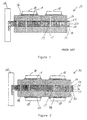
- FIG. 1 a typical prior-art printed wiring board structure 10 is shown.
- This printed wiring board structure 10 is configured with a conventional card rail 12, and has positioned on either side of a core 14 a plurality of polyamide circuit layers 16 including chip components 18 as known in the art.
- This prior art core 14 has a molybdenum center layer 20 with respective copper layers 22, 24 disposed above and below the molybdenum center layer 20.
- the copper-molybdenum-copper core 14 is generally satisfactory with respect to tensile modulus, thermal conductivity, and thermal expansion considerations, but is of a weight that can be highly disadvantageous depending upon particular applications.
- Plated through holes 15 are shown with hole fill 17 disposed thereabout through the core 14. Conventional blind vias 19 are shown.
- Figure 2 illustrates the preferred embodiment of the present invention.
- Figure 2 shows a printed wiring board structure 30 configured with a conventional card rail 12, a novel core 32, and polyamide circuit layers 16 including chip components 18.
- the core 32 is fabricated of a metal matrix 34 having disposed therein continuous pitch-based graphite fibers 36 substantially unidirectionally oriented and generally uniformly disposed throughout the matrix 34.
- a core 32 of this construction has a coefficient of thermal expansion (CTE) between about 3 and 6 ppm/°C and supports the low CTE required for surface mount technology solder joint reliability.
- CTE coefficient of thermal expansion
- the respective chip-carrying layers 16 and core 32 of the embodiments of Figure 2 have interfaces 52 therebetween and are electrically connected to each other (as required) through vias 48 extending between the layers 16 and core 32 which are plated with thermally conductive material 50 to thereby provide a plurality of connection sites along this interface to accommodate heat transfer to the core 32 for dissipation therefrom as described above and in addition to thermal vias 50.
- the preferred embodiment 30 has favorable characteristics with respect to high tensile modulus, high thermal conductivities, low coefficients of thermal expansion, and light weights.
- the pitch-based graphite fiber segments 36 of the core 32 especially provide extremely high tensile modulus, high thermal conductivity, low density, and selectable coefficient of thermal expansion of the core 32 obtainable by varying the fiber volume, fiber grade and fiber orientation during core manufacture.
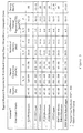
- the table shown in Figure 3 non-limitedly exemplifies construction variability and selectability, with the fiber grade designations identifying fiber products from Amoco Corporation, Chicago, Illinois. Because of the plurality and conductivity of connections along the respective interfaces 52, the present invention provides novel temperature control and circuit density since every connection results in heat transfer to the core 32.
Landscapes
- Engineering & Computer Science (AREA)
- Microelectronics & Electronic Packaging (AREA)
- Structure Of Printed Boards (AREA)
- Insulated Metal Substrates For Printed Circuits (AREA)
- Cooling Or The Like Of Semiconductors Or Solid State Devices (AREA)
- Manufacture Of Alloys Or Alloy Compounds (AREA)
Abstract
Description
Claims (5)
- A printed wiring board structure comprising at least one chip-carrying layer adjacent a core fabricated of a metal matrix having disposed therein pitch based graphite fibers, with said layer and said core having an interface therebetween and wherein the layer is integrally connected along said interface at a plurality of connection sites to the core at a plurality of vias each plated with a thermally and electrically conductive material and extending between the layer and the core.
- A printed wiring board structure as claimed in Claim 1 wherein the metal matrix of the core is an aluminum material.
- A printed wiring board structure as claimed in Claim 1 wherein the metal matrix of the core is a copper material.
- A printed wiring board structure as claimed in Claim 1 comprising two chip-carrying layers each on opposite sides of the core and each adjacent thereto, with each of said layers and said core having respective interfaces therebetween and wherein each layer is integrally connected along each said respective interface at a plurality of connection sites to the core at a plurality of vias each plated with a thermally conductive material and extending between said layer and the core.
- A printed wiring board structure as claimed in Claim 1 wherein at least one additional chip-carrying layer is layerly affixed to at least one chip carrying layer connected to the core.
Applications Claiming Priority (2)
| Application Number | Priority Date | Filing Date | Title |
|---|---|---|---|
| US324288 | 1994-10-14 | ||
| US09/324,288 US6340796B1 (en) | 1999-06-02 | 1999-06-02 | Printed wiring board structure with integral metal matrix composite core |
Publications (3)
| Publication Number | Publication Date |
|---|---|
| EP1058491A2 true EP1058491A2 (en) | 2000-12-06 |
| EP1058491A3 EP1058491A3 (en) | 2002-03-13 |
| EP1058491B1 EP1058491B1 (en) | 2005-11-02 |
Family
ID=23262946
Family Applications (1)
| Application Number | Title | Priority Date | Filing Date |
|---|---|---|---|
| EP00304651A Expired - Lifetime EP1058491B1 (en) | 1999-06-02 | 2000-05-31 | Printed wiring board structure with integral metal matrix composite core |
Country Status (3)
| Country | Link |
|---|---|
| US (1) | US6340796B1 (en) |
| EP (1) | EP1058491B1 (en) |
| DE (1) | DE60023597T2 (en) |
Families Citing this family (20)
| Publication number | Priority date | Publication date | Assignee | Title |
|---|---|---|---|---|
| JP3812321B2 (en) * | 2000-10-25 | 2006-08-23 | 株式会社豊田自動織機 | Heat sink and manufacturing method thereof |
| USRE44438E1 (en) | 2001-02-27 | 2013-08-13 | Stats Chippac, Ltd. | Semiconductor device and method of dissipating heat from thin package-on-package mounted to substrate |
| US20020121707A1 (en) * | 2001-02-27 | 2002-09-05 | Chippac, Inc. | Super-thin high speed flip chip package |
| US8143108B2 (en) * | 2004-10-07 | 2012-03-27 | Stats Chippac, Ltd. | Semiconductor device and method of dissipating heat from thin package-on-package mounted to substrate |
| US7038142B2 (en) * | 2002-01-24 | 2006-05-02 | Fujitsu Limited | Circuit board and method for fabricating the same, and electronic device |
| WO2005117508A2 (en) * | 2004-05-15 | 2005-12-08 | C-Core Technologies, Inc. | Printed wiring board with conductive constraining core including resin filled channels |
| JP4556174B2 (en) * | 2004-12-15 | 2010-10-06 | 日本電気株式会社 | Portable terminal device and heat dissipation method |
| KR20070112274A (en) * | 2005-03-15 | 2007-11-22 | 씨-코어 테크놀로지즈, 인코포레이티드 | How to Configure a Suppression Core Material in a Printed Wiring Board |
| USRE45637E1 (en) | 2005-08-29 | 2015-07-28 | Stablcor Technology, Inc. | Processes for manufacturing printed wiring boards |
| US7730613B2 (en) * | 2005-08-29 | 2010-06-08 | Stablcor, Inc. | Processes for manufacturing printed wiring boards |
| US8203080B2 (en) | 2006-07-14 | 2012-06-19 | Stablcor Technology, Inc. | Build-up printed wiring board substrate having a core layer that is part of a circuit |
| JP2009088173A (en) * | 2007-09-28 | 2009-04-23 | Fujitsu Ltd | Wiring board |
| WO2009065105A2 (en) * | 2007-11-16 | 2009-05-22 | Continental Automotive Systems Us, Inc. | Thermal packaging of transmission controller using carbon composite printed circuit board material |
| KR101148628B1 (en) * | 2008-11-20 | 2012-05-25 | 후지쯔 가부시끼가이샤 | Wiring board and method for producing wiring board |
| WO2010146652A1 (en) * | 2009-06-15 | 2010-12-23 | 富士通オプティカルコンポーネンツ株式会社 | Optical module |
| US9332632B2 (en) | 2014-08-20 | 2016-05-03 | Stablcor Technology, Inc. | Graphene-based thermal management cores and systems and methods for constructing printed wiring boards |
| KR101841836B1 (en) * | 2016-07-05 | 2018-03-26 | 김구용 | PCB module having multi-directional heat-radiation structure, and radiation plate, multi-layer PCB assembly, and module case used in the same PCB module |
| JP7121027B2 (en) * | 2017-09-28 | 2022-08-17 | 京セラ株式会社 | Substrate for mounting electronic element and electronic device |
| US10790241B2 (en) | 2019-02-28 | 2020-09-29 | Advanced Semiconductor Engineering, Inc. | Wiring structure and method for manufacturing the same |
| US11171118B2 (en) * | 2019-07-03 | 2021-11-09 | Micron Technology, Inc. | Semiconductor assemblies including thermal circuits and methods of manufacturing the same |
Family Cites Families (27)
| Publication number | Priority date | Publication date | Assignee | Title |
|---|---|---|---|---|
| DE2206700B2 (en) | 1972-02-12 | 1976-07-01 | Sigri Elektrographit Gmbh, 8901 Meitingen | METHOD FOR MANUFACTURING FIBER-REINFORCED COMPOSITE BODIES |
| US4318954A (en) | 1981-02-09 | 1982-03-09 | Boeing Aerospace Company | Printed wiring board substrates for ceramic chip carriers |
| FR2546878B1 (en) * | 1983-05-31 | 1988-04-08 | Slonina Jean Pierre | SUPPORT PLATE FOR A LIGHT CERAMIC SUBSTRATE WITH HIGH THERMAL CONDUCTIVITY AND EXPANSION COEFFICIENT SUITABLE FOR ALL APPLICATIONS IN THE ELECTRONIC FIELD |
| US4609586A (en) | 1984-08-02 | 1986-09-02 | The Boeing Company | Thermally conductive printed wiring board laminate |
| US4654248A (en) | 1985-12-16 | 1987-03-31 | Gte Communication Systems Corporation | Printed wiring board with zones of controlled thermal coefficient of expansion |
| US4867235A (en) | 1986-10-20 | 1989-09-19 | Westinghouse Electric Corp. | Composite heat transfer means |
| US4849858A (en) * | 1986-10-20 | 1989-07-18 | Westinghouse Electric Corp. | Composite heat transfer means |
| US4791248A (en) | 1987-01-22 | 1988-12-13 | The Boeing Company | Printed wire circuit board and its method of manufacture |
| US4806704A (en) * | 1987-06-08 | 1989-02-21 | General Electric Company | Metal matrix composite and structure using metal matrix composites for electronic applications |
| US5002823A (en) | 1987-06-12 | 1991-03-26 | E. I. Du Pont De Nemours And Company | Reinforced composites having improved flex fatigue life |
| US4963697A (en) | 1988-02-12 | 1990-10-16 | Texas Instruments Incorporated | Advanced polymers on metal printed wiring board |
| US4882454A (en) | 1988-02-12 | 1989-11-21 | Texas Instruments Incorporated | Thermal interface for a printed wiring board |
| DE8813093U1 (en) * | 1988-10-18 | 1988-12-08 | Teldix Gmbh, 69123 Heidelberg | Circuit board |
| US5224017A (en) * | 1989-05-17 | 1993-06-29 | The Charles Stark Draper Laboratory, Inc. | Composite heat transfer device |
| US5716663A (en) | 1990-02-09 | 1998-02-10 | Toranaga Technologies | Multilayer printed circuit |
| TW210422B (en) | 1991-06-04 | 1993-08-01 | Akzo Nv | |
| JPH05110219A (en) * | 1991-10-17 | 1993-04-30 | Mitsubishi Electric Corp | Printed wiring board |
| US5296310A (en) | 1992-02-14 | 1994-03-22 | Materials Science Corporation | High conductivity hydrid material for thermal management |
| US5306571A (en) * | 1992-03-06 | 1994-04-26 | Bp Chemicals Inc., Advanced Materials Division | Metal-matrix-composite |
| FR2694139B1 (en) * | 1992-07-21 | 1994-10-14 | Aerospatiale | Interconnection substrate for electronic components and its manufacturing process. |
| US5544017A (en) | 1992-08-05 | 1996-08-06 | Fujitsu Limited | Multichip module substrate |
| US5309629A (en) | 1992-09-01 | 1994-05-10 | Rogers Corporation | Method of manufacturing a multilayer circuit board |
| GB9225260D0 (en) | 1992-12-03 | 1993-01-27 | Int Computers Ltd | Cooling electronic circuit assemblies |
| US5840402A (en) | 1994-06-24 | 1998-11-24 | Sheldahl, Inc. | Metallized laminate material having ordered distribution of conductive through holes |
| US5571608A (en) | 1994-07-15 | 1996-11-05 | Dell Usa, L.P. | Apparatus and method of making laminate an embedded conductive layer |
| US5699613A (en) | 1995-09-25 | 1997-12-23 | International Business Machines Corporation | Fine dimension stacked vias for a multiple layer circuit board structure |
| JPH11145334A (en) * | 1997-09-02 | 1999-05-28 | Eastern Co Ltd | Wiring board |
-
1999
- 1999-06-02 US US09/324,288 patent/US6340796B1/en not_active Expired - Lifetime
-
2000
- 2000-05-31 EP EP00304651A patent/EP1058491B1/en not_active Expired - Lifetime
- 2000-05-31 DE DE60023597T patent/DE60023597T2/en not_active Expired - Lifetime
Also Published As
| Publication number | Publication date |
|---|---|
| DE60023597D1 (en) | 2005-12-08 |
| US6340796B1 (en) | 2002-01-22 |
| DE60023597T2 (en) | 2006-07-20 |
| EP1058491A3 (en) | 2002-03-13 |
| EP1058491B1 (en) | 2005-11-02 |
Similar Documents
| Publication | Publication Date | Title |
|---|---|---|
| US6207904B1 (en) | Printed wiring board structure having continuous graphite fibers | |
| US6340796B1 (en) | Printed wiring board structure with integral metal matrix composite core | |
| US4849858A (en) | Composite heat transfer means | |
| EP0147014B1 (en) | Multilayer printed circuit board structure | |
| US4811166A (en) | Heat dissipating member for mounting a semiconductor device and electrical circuit unit incorporating the member | |
| US4963414A (en) | Low thermal expansion, heat sinking substrate for electronic surface mount applications | |
| US4609586A (en) | Thermally conductive printed wiring board laminate | |
| US5675474A (en) | Highly heat-radiating ceramic package | |
| US4867235A (en) | Composite heat transfer means | |
| US5224017A (en) | Composite heat transfer device | |
| US7038313B2 (en) | Semiconductor device and method of manufacturing the same | |
| US4812792A (en) | High-frequency multilayer printed circuit board | |
| US4689110A (en) | Method of fabricating multilayer printed circuit board structure | |
| US6986454B2 (en) | Electronic package having controlled height stand-off solder joint | |
| US6317331B1 (en) | Wiring substrate with thermal insert | |
| JP2009164582A (en) | Lightweight circuit board with conductive constraining core | |
| KR20080065988A (en) | Heat sink module and its manufacturing method | |
| US6671176B1 (en) | Method of cooling heat-generating electrical components | |
| US20070012477A1 (en) | Electronic component package including joint material having higher heat conductivity | |
| US7161240B2 (en) | Insitu-cooled electrical assemblage | |
| US5002715A (en) | Method for the fabrication of a heat transfer member for electronic systems | |
| KR20250111156A (en) | Woven pyrolytic graphite sheets for heat diffusion | |
| Dance et al. | Clad metal circuit board substrates for direct mounting of ceramic chip carriers | |
| US6228470B1 (en) | Composite substrate for electronic components | |
| JPH10256428A (en) | Semiconductor package |
Legal Events
| Date | Code | Title | Description |
|---|---|---|---|
| PUAI | Public reference made under article 153(3) epc to a published international application that has entered the european phase |
Free format text: ORIGINAL CODE: 0009012 |
|
| AK | Designated contracting states |
Kind code of ref document: A2 Designated state(s): DE FR GB Kind code of ref document: A2 Designated state(s): AT BE CH CY DE DK ES FI FR GB GR IE IT LI LU MC NL PT SE |
|
| AX | Request for extension of the european patent |
Free format text: AL;LT;LV;MK;RO;SI |
|
| PUAL | Search report despatched |
Free format text: ORIGINAL CODE: 0009013 |
|
| AK | Designated contracting states |
Kind code of ref document: A3 Designated state(s): AT BE CH CY DE DK ES FI FR GB GR IE IT LI LU MC NL PT SE |
|
| AX | Request for extension of the european patent |
Free format text: AL;LT;LV;MK;RO;SI |
|
| 17P | Request for examination filed |
Effective date: 20020605 |
|
| AKX | Designation fees paid |
Free format text: DE FR GB |
|
| 17Q | First examination report despatched |
Effective date: 20041006 |
|
| GRAP | Despatch of communication of intention to grant a patent |
Free format text: ORIGINAL CODE: EPIDOSNIGR1 |
|
| GRAS | Grant fee paid |
Free format text: ORIGINAL CODE: EPIDOSNIGR3 |
|
| GRAA | (expected) grant |
Free format text: ORIGINAL CODE: 0009210 |
|
| AK | Designated contracting states |
Kind code of ref document: B1 Designated state(s): DE FR GB |
|
| REG | Reference to a national code |
Ref country code: GB Ref legal event code: FG4D |
|
| REF | Corresponds to: |
Ref document number: 60023597 Country of ref document: DE Date of ref document: 20051208 Kind code of ref document: P |
|
| ET | Fr: translation filed | ||
| PLBE | No opposition filed within time limit |
Free format text: ORIGINAL CODE: 0009261 |
|
| STAA | Information on the status of an ep patent application or granted ep patent |
Free format text: STATUS: NO OPPOSITION FILED WITHIN TIME LIMIT |
|
| 26N | No opposition filed |
Effective date: 20060803 |
|
| REG | Reference to a national code |
Ref country code: GB Ref legal event code: 732E Free format text: REGISTERED BETWEEN 20110428 AND 20110504 |
|
| REG | Reference to a national code |
Ref country code: FR Ref legal event code: TP Owner name: NORTHROP GRUMMAN SYSTEMS CORPORATION, US Effective date: 20120314 |
|
| REG | Reference to a national code |
Ref country code: DE Ref legal event code: R081 Ref document number: 60023597 Country of ref document: DE Owner name: NORTHROP GRUMMAN SYSTEMS CORPORATION (N.D.GES., US Free format text: FORMER OWNER: NORTHROP GRUMMAN CORP., LOS ANGELES, US Effective date: 20130205 Ref country code: DE Ref legal event code: R081 Ref document number: 60023597 Country of ref document: DE Owner name: NORTHROP GRUMMAN SYSTEMS CORPORATION (N.D.GES., US Free format text: FORMER OWNER: NORTHROP GRUMMAN CORP., LOS ANGELES, CALIF., US Effective date: 20130205 |
|
| REG | Reference to a national code |
Ref country code: FR Ref legal event code: PLFP Year of fee payment: 17 |
|
| REG | Reference to a national code |
Ref country code: FR Ref legal event code: PLFP Year of fee payment: 18 |
|
| REG | Reference to a national code |
Ref country code: FR Ref legal event code: PLFP Year of fee payment: 19 |
|
| PGFP | Annual fee paid to national office [announced via postgrant information from national office to epo] |
Ref country code: DE Payment date: 20190521 Year of fee payment: 20 |
|
| PGFP | Annual fee paid to national office [announced via postgrant information from national office to epo] |
Ref country code: FR Payment date: 20190522 Year of fee payment: 20 |
|
| PGFP | Annual fee paid to national office [announced via postgrant information from national office to epo] |
Ref country code: GB Payment date: 20190521 Year of fee payment: 20 |
|
| REG | Reference to a national code |
Ref country code: DE Ref legal event code: R071 Ref document number: 60023597 Country of ref document: DE |
|
| REG | Reference to a national code |
Ref country code: GB Ref legal event code: PE20 Expiry date: 20200530 |
|
| PG25 | Lapsed in a contracting state [announced via postgrant information from national office to epo] |
Ref country code: GB Free format text: LAPSE BECAUSE OF EXPIRATION OF PROTECTION Effective date: 20200530 |