EP1058373A1 - Protection circuit for a switch, and a switched-mode power supply - Google Patents
Protection circuit for a switch, and a switched-mode power supply Download PDFInfo
- Publication number
- EP1058373A1 EP1058373A1 EP00108757A EP00108757A EP1058373A1 EP 1058373 A1 EP1058373 A1 EP 1058373A1 EP 00108757 A EP00108757 A EP 00108757A EP 00108757 A EP00108757 A EP 00108757A EP 1058373 A1 EP1058373 A1 EP 1058373A1
- Authority
- EP
- European Patent Office
- Prior art keywords
- switched
- protection circuit
- energy
- switch
- storage means
- Prior art date
- Legal status (The legal status is an assumption and is not a legal conclusion. Google has not performed a legal analysis and makes no representation as to the accuracy of the status listed.)
- Withdrawn
Links
- 238000004146 energy storage Methods 0.000 claims abstract description 26
- 239000003990 capacitor Substances 0.000 claims abstract description 17
- 238000004804 winding Methods 0.000 claims description 11
- 238000002955 isolation Methods 0.000 description 3
- 230000007547 defect Effects 0.000 description 2
- 238000005259 measurement Methods 0.000 description 2
- 230000001360 synchronised effect Effects 0.000 description 2
- 230000005540 biological transmission Effects 0.000 description 1
- 230000001419 dependent effect Effects 0.000 description 1
- 238000011161 development Methods 0.000 description 1
- 230000018109 developmental process Effects 0.000 description 1
- 238000010586 diagram Methods 0.000 description 1
- 238000001914 filtration Methods 0.000 description 1
- 238000000034 method Methods 0.000 description 1
- 230000010355 oscillation Effects 0.000 description 1
- 238000010079 rubber tapping Methods 0.000 description 1
- 238000011144 upstream manufacturing Methods 0.000 description 1
Images
Classifications
-
- H—ELECTRICITY
- H02—GENERATION; CONVERSION OR DISTRIBUTION OF ELECTRIC POWER
- H02M—APPARATUS FOR CONVERSION BETWEEN AC AND AC, BETWEEN AC AND DC, OR BETWEEN DC AND DC, AND FOR USE WITH MAINS OR SIMILAR POWER SUPPLY SYSTEMS; CONVERSION OF DC OR AC INPUT POWER INTO SURGE OUTPUT POWER; CONTROL OR REGULATION THEREOF
- H02M1/00—Details of apparatus for conversion
- H02M1/32—Means for protecting converters other than automatic disconnection
-
- H—ELECTRICITY
- H03—ELECTRONIC CIRCUITRY
- H03K—PULSE TECHNIQUE
- H03K17/00—Electronic switching or gating, i.e. not by contact-making and –breaking
- H03K17/08—Modifications for protecting switching circuit against overcurrent or overvoltage
- H03K17/081—Modifications for protecting switching circuit against overcurrent or overvoltage without feedback from the output circuit to the control circuit
- H03K17/0812—Modifications for protecting switching circuit against overcurrent or overvoltage without feedback from the output circuit to the control circuit by measures taken in the control circuit
- H03K17/08122—Modifications for protecting switching circuit against overcurrent or overvoltage without feedback from the output circuit to the control circuit by measures taken in the control circuit in field-effect transistor switches
Definitions
- the present invention relates to a protection circuit for switches, in particular such as those which are used in switched-mode power supplies, and to a switched-mode power supply relating to this.
- Switches with a high-impedance control input are increasingly being used in switched-mode power supplies.
- the high impedance of the control input means that the switched-mode power supply can enter an undefined state in the event of a defect, which state can destroy the switch. This is possible, for example, in the event of a short circuit at the output of the switched-mode power supply or in the event of an interruption in the switched-mode power supply control loop, resulting in an interruption in the closed-loop-controlled switch operation.
- a residual voltage may still be present at the control input of the switch, in the case of switched-mode power supplies, due, in particular, to their starting circuit, so that the switch is partially actuated. If the switch is only partially actuated, a high current flows through it when a voltage is still at the same time applied to it, so that its power loss becomes excessive and, in consequence, it is destroyed.
- DE 197 35 208 A1 discloses a free-running switched-mode power supply having a protection circuit which reliably switches the switching transistor off when a short circuit occurs.
- the control voltage at the input of the switching transistor is dissipated through a transistor stage, so that the switching transistor reliably remains switched off in the event of a short circuit.
- the object of the present invention is to specify a protection circuit and a switched-mode power supply relating to this for a switch, which protection circuit prevents the switch from being actuated, and thus prevents it from being destroyed, in the event of a fault.
- the protection circuit of the present invention contains an energy-storage means which is connected to the control input of the switch and is charged with a delay via resistance means when a control voltage is present, and is then discharged via switching means when the control voltage is absent or low. Since switches of this type are normally actuated by square-wave voltages which are, for example, pulse-width modulated or whose frequency is variable for control of a switched-mode power supply, the energy-storage means is in this way charged slowly during the on-signal for the switch, but is discharged once again in the same way during the "off" signal. It is thus impossible for a higher voltage to build up across the energy-storage means during normal switch operation.
- the protection circuit also contains a switching stage which is connected to a supply voltage for the switch, switches on when there is a specific threshold voltage across the energy-storage means, and in consequence reduces the supply voltage.
- the energy-storage means is, for example, a capacitor
- the switching stage is a single transistor stage or a pair of transistors connected in the form of a thyristor circuit.
- the energy-storage means When the switching stage is switched on at the said threshold voltage, the energy-storage means is at the same time discharged via the switching stage. A portion of the charge dissipated from the supply voltage is in this case at least partially routed to the energy-storage means, so that the phase during which the switching stage is switched on is lengthened. This is achieved by means of a diode in parallel with the energy-storage means. This diode at the same time prevents inverse charging of the energy-storage means.
- the protection circuit can be used, in particular, for switched-mode power supplies such as those used in television sets or video recorders, for example.
- Switched-mode power supplies of this type normally have a supply voltage which is fed from a secondary winding of the transformer, and a starting circuit which supplies a supply voltage once the switched-mode power supply is switched on, until the switched-mode power supply supplies itself via the supply stage.
- a control voltage is applied to the control input of the switch, by means of which the switched-mode power supply stabilizes output voltages via a control circuit arranged either on the secondary side or the primary side.
- the control input is decoupled from the starting circuit and from the supply stage via a resistance means.
- the energy-storage means in the protection circuit is in this case connected to the control input of the switching transistor, and the switching stage is connected to the starting circuit and to the supply stage.
- a low-impedance current-measurement resistor is often connected downstream from the output of the switch in a switched-mode power supply, to supply current information for the control circuit.
- the output of the protection circuit is then advantageously connected to the higher-potential output of the switching transistor, rather than to earth.
- the switched-mode power supply in the figure is connected via a mains connection 1 to the electrical mains system, whose mains voltage is present in an input stage 2, which, in particular, contains filters for filtering undesirable high-frequency voltages.
- the mains voltage is then rectified in a circuit 3, and is buffered via an energy-storage capacitor for operation of the switched-mode power supply.
- This voltage is applied via the primary winding W1 of a transformer Tr to a switch T1, in this exemplary embodiment a MOSFET.
- the switch T1 is switched on and off cyclically during operation by means of a square-wave control voltage Ug, in order to transmit power to secondary windings W2 and W3 of the transformer Tr.
- the winding W3 is in this case arranged on the primary side and is used, via a supply circuit 5, to provide a supply voltage VCC for operation of the switched-mode power supply.
- the voltage emitted from the winding W2 arranged on the secondary side is rectified via a diode Da and is stabilized by a capacitor Ca in order to supply an external load.
- the output voltage is stabilized by tapping it off and transmitting it to a control circuit 7 on the primary side via an optocoupler 6 (or else via other transmission means, since the switched-mode power supply provides mains isolation in this exemplary embodiment).
- This control circuit 7 controls the control input G of the switching transistor T1.
- the control circuit 7 is indicated only schematically and may, in particular, also be arranged on the secondary side. It may contain, for example, an integrated circuit with an oscillator, or else may be operated at a synchronized frequency.
- the switched-mode power supply may be in the form of a free-running switched-mode power supply.
- the switched-mode power supply also contains a current-measurement resistor Rs, via which the output of the switching transistor T1 is connected to earth M and which provides current information for the control circuit 7, relating to the magnitude of the current flowing through the switching transistor T1.
- the switched-mode power supply furthermore contains a starting circuit having a resistor or a resistor chain Rm, which provides a starting current Im in order to start the switched-mode power supply, until the switched-mode power supply supplies itself via the supply stage 5.
- This starting circuit may be connected either upstream or downstream of the energy-storage capacitor and the rectifier in the circuit 3.
- the switched-mode power supply contains a so-called snubber network 4 in parallel with the primary winding W1, which damps switching spikes when the switching transistor T1 switches off.
- the protection circuit is connected to the control input G of the switching transistor T1, whose control voltage Ug is monitored.
- a capacitor C1 in the protection circuit is charged slowly via a resistor R1.
- the capacitor C1 is discharged quickly again via a diode D1, so that it is impossible for any increased voltage to build up across the capacitor C1 during normal operation.
- the diode D1 operates as a switching means and, for example, a controlled transistor may also be used as an alternative.
- the control input of a transistor T2 is connected to the capacitor C1 so that, when the transistor T2 is switched on, the supply voltage VCC is reduced to a lower potential via a further transistor T3.
- the two transistors T2 and T3 are in this case connected as a thyristor stage, so that the switching-on process is carried out quickly and effectively.
- the transistor T2 is always switched off, since sufficient voltage to switch the transistor T2 on does not build up across the capacitor C1, as explained above.
- a capacitor C2 and a resistor R3, connected in parallel with it, are connected to the control input of the transistor T3, so that any disturbance voltage which may occur cannot cause the transistor T3 to switch on, thus switching off the switched-mode power supply.
- a further dangerous fault situation is a failure of the control stage 7 in such a manner that it and thus the input G of the switching transistor T1, have a high impedance.
- the control voltage Ug rises continuously, due to the starting current Im.
- the voltage across the capacitor C1 rises until a specific threshold voltage is reached, at which the transistor T2 switches on.
- the supply voltage VCC being reduced or dissipated via the transistor T3, as a result of which the control voltage Ug across the resistor Rg falls until the switching transistor T1 switches off again.
- the output of the transistor T3 in this exemplary embodiment is, however, not connected directly to earth, but via a resistor R2 to the output of the switching transistor T1, which is connected via the resistor Rs to earth M.
- the transistor T3 switches on, then the voltage across R2 raises the voltage across C1, so that the transistor T2 is actuated for a longer period, and the supply voltage VCC is substantially reduced.
- the capacitor C1 is completely discharged via the transistor T2 and a diode D3.
- the protection circuit carries out a reset operation, so to speak, so that the switching transistor T1 can resume operation after a certain time. However, if the fault situation is still present, then the protection circuit responds once again.
- the voltage at which the switching transistor T1 switches on is 5 V.
- VCC is equal to 14 V.
- the threshold voltage is approximately 1.2 volts, and is governed by the base-emitter voltage of T2 and the voltage at which the diode D3 becomes forward-biased. In normal operation, the diode D1 becomes forward-biased at a voltage of about 0.6 volts. If the supply voltage VCC falls to about 1.8 volts, then T2 and T3 are switched off again.
- the switched-mode power supply in the figure is in the form of a free-running switched-mode power supply.
- the protection circuit may equally well be used for other switched-mode power supplies, for example for synchronized switched-mode power supplies. It can be used not only for switched-mode power supplies with mains isolation, but also for those without mains isolation, for example DC/DC converters.
Landscapes
- Engineering & Computer Science (AREA)
- Power Engineering (AREA)
- Dc-Dc Converters (AREA)
Abstract
Description
- The present invention relates to a protection circuit for switches, in particular such as those which are used in switched-mode power supplies, and to a switched-mode power supply relating to this.
- Switches with a high-impedance control input, such as MOSFETs for example, are increasingly being used in switched-mode power supplies. The high impedance of the control input means that the switched-mode power supply can enter an undefined state in the event of a defect, which state can destroy the switch. This is possible, for example, in the event of a short circuit at the output of the switched-mode power supply or in the event of an interruption in the switched-mode power supply control loop, resulting in an interruption in the closed-loop-controlled switch operation. However, in cases such as this, a residual voltage may still be present at the control input of the switch, in the case of switched-mode power supplies, due, in particular, to their starting circuit, so that the switch is partially actuated. If the switch is only partially actuated, a high current flows through it when a voltage is still at the same time applied to it, so that its power loss becomes excessive and, in consequence, it is destroyed.
- DE 197 35 208 A1 discloses a free-running switched-mode power supply having a protection circuit which reliably switches the switching transistor off when a short circuit occurs. In one exemplary embodiment, the control voltage at the input of the switching transistor is dissipated through a transistor stage, so that the switching transistor reliably remains switched off in the event of a short circuit.
- The object of the present invention is to specify a protection circuit and a switched-mode power supply relating to this for a switch, which protection circuit prevents the switch from being actuated, and thus prevents it from being destroyed, in the event of a fault.
- This object is achieved by the invention specified in Claims 1 and 8. Advantageous developments of the invention are specified in the dependent claims.
- The protection circuit of the present invention contains an energy-storage means which is connected to the control input of the switch and is charged with a delay via resistance means when a control voltage is present, and is then discharged via switching means when the control voltage is absent or low. Since switches of this type are normally actuated by square-wave voltages which are, for example, pulse-width modulated or whose frequency is variable for control of a switched-mode power supply, the energy-storage means is in this way charged slowly during the on-signal for the switch, but is discharged once again in the same way during the "off" signal. It is thus impossible for a higher voltage to build up across the energy-storage means during normal switch operation.
- The protection circuit also contains a switching stage which is connected to a supply voltage for the switch, switches on when there is a specific threshold voltage across the energy-storage means, and in consequence reduces the supply voltage. The energy-storage means is, for example, a capacitor, and the switching stage is a single transistor stage or a pair of transistors connected in the form of a thyristor circuit.
- When the switching stage is switched on at the said threshold voltage, the energy-storage means is at the same time discharged via the switching stage. A portion of the charge dissipated from the supply voltage is in this case at least partially routed to the energy-storage means, so that the phase during which the switching stage is switched on is lengthened. This is achieved by means of a diode in parallel with the energy-storage means. This diode at the same time prevents inverse charging of the energy-storage means.
- The protection circuit can be used, in particular, for switched-mode power supplies such as those used in television sets or video recorders, for example. Switched-mode power supplies of this type normally have a supply voltage which is fed from a secondary winding of the transformer, and a starting circuit which supplies a supply voltage once the switched-mode power supply is switched on, until the switched-mode power supply supplies itself via the supply stage.
- A control voltage is applied to the control input of the switch, by means of which the switched-mode power supply stabilizes output voltages via a control circuit arranged either on the secondary side or the primary side. The control input is decoupled from the starting circuit and from the supply stage via a resistance means. The energy-storage means in the protection circuit is in this case connected to the control input of the switching transistor, and the switching stage is connected to the starting circuit and to the supply stage.
- In the event of a fault, a situation may arise in which the closed-loop-controlled switch operation is interrupted and a voltage builds up, for example due to the starting circuit, at the control input of the switch, and this voltage could at least partially switch the switch on. This is identified by the protection circuit, and the supply voltage and the voltage at the control input of the switch are reduced appropriately by the protection circuit, so that there is no risk to the switch.
- A low-impedance current-measurement resistor is often connected downstream from the output of the switch in a switched-mode power supply, to supply current information for the control circuit. The output of the protection circuit is then advantageously connected to the higher-potential output of the switching transistor, rather than to earth.
- The invention will be explained in more detail in the following text using, by way of example, a schematic circuit diagram, in which:
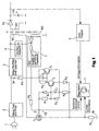
- The figure shows a switched-mode power supply having a protection circuit.
-
- The switched-mode power supply in the figure is connected via a mains connection 1 to the electrical mains system, whose mains voltage is present in an
input stage 2, which, in particular, contains filters for filtering undesirable high-frequency voltages. The mains voltage is then rectified in acircuit 3, and is buffered via an energy-storage capacitor for operation of the switched-mode power supply. - This voltage is applied via the primary winding W1 of a transformer Tr to a switch T1, in this exemplary embodiment a MOSFET. The switch T1 is switched on and off cyclically during operation by means of a square-wave control voltage Ug, in order to transmit power to secondary windings W2 and W3 of the transformer Tr. The winding W3 is in this case arranged on the primary side and is used, via a
supply circuit 5, to provide a supply voltage VCC for operation of the switched-mode power supply. - The voltage emitted from the winding W2 arranged on the secondary side is rectified via a diode Da and is stabilized by a capacitor Ca in order to supply an external load. The output voltage is stabilized by tapping it off and transmitting it to a control circuit 7 on the primary side via an optocoupler 6 (or else via other transmission means, since the switched-mode power supply provides mains isolation in this exemplary embodiment). This control circuit 7 controls the control input G of the switching transistor T1. The control circuit 7 is indicated only schematically and may, in particular, also be arranged on the secondary side. It may contain, for example, an integrated circuit with an oscillator, or else may be operated at a synchronized frequency. Furthermore, the switched-mode power supply may be in the form of a free-running switched-mode power supply.
- The switched-mode power supply also contains a current-measurement resistor Rs, via which the output of the switching transistor T1 is connected to earth M and which provides current information for the control circuit 7, relating to the magnitude of the current flowing through the switching transistor T1.
- The switched-mode power supply furthermore contains a starting circuit having a resistor or a resistor chain Rm, which provides a starting current Im in order to start the switched-mode power supply, until the switched-mode power supply supplies itself via the
supply stage 5. This starting circuit may be connected either upstream or downstream of the energy-storage capacitor and the rectifier in thecircuit 3. Furthermore, the switched-mode power supply contains a so-calledsnubber network 4 in parallel with the primary winding W1, which damps switching spikes when the switching transistor T1 switches off. - The protection circuit is connected to the control input G of the switching transistor T1, whose control voltage Ug is monitored. During the "on" phase of the switching transistor T1, a capacitor C1 in the protection circuit is charged slowly via a resistor R1. During the "off" phase of the switching transistor, the capacitor C1 is discharged quickly again via a diode D1, so that it is impossible for any increased voltage to build up across the capacitor C1 during normal operation. In this case, the diode D1 operates as a switching means and, for example, a controlled transistor may also be used as an alternative.
- The control input of a transistor T2 is connected to the capacitor C1 so that, when the transistor T2 is switched on, the supply voltage VCC is reduced to a lower potential via a further transistor T3. The two transistors T2 and T3 are in this case connected as a thyristor stage, so that the switching-on process is carried out quickly and effectively. When the switched-mode power supply is operating normally, the transistor T2 is always switched off, since sufficient voltage to switch the transistor T2 on does not build up across the capacitor C1, as explained above. A capacitor C2 and a resistor R3, connected in parallel with it, are connected to the control input of the transistor T3, so that any disturbance voltage which may occur cannot cause the transistor T3 to switch on, thus switching off the switched-mode power supply.
- Closed-loop-controlled switching operation is disturbed in the event of a short circuit on the output side, or else in the event of some other fault, such as an interruption in the control loop. In the event of a short circuit, for example, the control circuit 7 thus tries to switch the switching transistor T1 on for as long as possible, in order in this way to raise the output voltage. This allows the switching transistor T1 to be overloaded.
- A further dangerous fault situation is a failure of the control stage 7 in such a manner that it and thus the input G of the switching transistor T1, have a high impedance. In this case, the control voltage Ug rises continuously, due to the starting current Im. However, in consequence, the voltage across the capacitor C1 rises until a specific threshold voltage is reached, at which the transistor T2 switches on. This results in the supply voltage VCC being reduced or dissipated via the transistor T3, as a result of which the control voltage Ug across the resistor Rg falls until the switching transistor T1 switches off again.
- The output of the transistor T3 in this exemplary embodiment is, however, not connected directly to earth, but via a resistor R2 to the output of the switching transistor T1, which is connected via the resistor Rs to earth M. When the transistor T3 switches on, then the voltage across R2 raises the voltage across C1, so that the transistor T2 is actuated for a longer period, and the supply voltage VCC is substantially reduced. A diode D2, in parallel with the capacitor C1, in this case prevents the polarity of C1 from being reversed. At the same time, the capacitor C1 is completely discharged via the transistor T2 and a diode D3.
- In consequence, the protection circuit carries out a reset operation, so to speak, so that the switching transistor T1 can resume operation after a certain time. However, if the fault situation is still present, then the protection circuit responds once again.
- All defects in which the output of the control circuit 7 still has a high impedance, so that a DC voltage builds up at the control input G, are problematic. This is also true if the oscillation of the switched-mode power supply breaks down and the supply voltage VCC is no longer provided via the secondary winding W3, since the starting circuit continues to remain active via the resistor Rm. Since the protection circuit responds cyclically, the switched-mode power supply can resume operation at any time, once the fault has been rectified. By raising the voltage across the capacitor C1 by means of the resistor R2, C1 is in this case always completely discharged in the event of a fault.
- In the exemplary embodiment illustrated in the figure, the component values are as follows:
R1 = 100 k C1 = 10 µF R2 = 470 R C2 = 10 µF R3 = 10 k Rm = 560 k Rg = 100 R Rs = 4 R7 - The voltage at which the switching transistor T1 switches on is 5 V. VCC is equal to 14 V.
- The threshold voltage is approximately 1.2 volts, and is governed by the base-emitter voltage of T2 and the voltage at which the diode D3 becomes forward-biased. In normal operation, the diode D1 becomes forward-biased at a voltage of about 0.6 volts. If the supply voltage VCC falls to about 1.8 volts, then T2 and T3 are switched off again.
- The switched-mode power supply in the figure is in the form of a free-running switched-mode power supply. However, the protection circuit may equally well be used for other switched-mode power supplies, for example for synchronized switched-mode power supplies. It can be used not only for switched-mode power supplies with mains isolation, but also for those without mains isolation, for example DC/DC converters.
Claims (10)
- Protection circuit for a switch (T1) in which case the protection circuit has an energy-storage means (C1) which is coupled to a control input (G) of the switch (T1) and which is charged with a delay via resistance means (R1) when a control voltage (Ug) is present and is discharged via switching means (D2) when the control voltage (Ug) is low or absent, and has a switching stage (T2, T3) which is coupled to a supply voltage (VCC), switches on at a specific threshold voltage across the energy-storage means (C1), and in consequence reduces the supply voltage (VCC).
- Protection circuit according to Claim 1, characterized in that the charge which is dissipated from the supply voltage (VCC) when the switching stage (T2, T3) is switched on is at least partially routed to the energy-storage means (C1), so that the phase during which the switching stage (T2, T3) is switched on is lengthened.
- Protection circuit according to Claim 2, characterized in that the dissipated charge is routed to the energy-storage means (C1) via a diode (D2) which is connected in parallel with the said energy-storage means (C1).
- Protection circuit according to Claim 1, 2 or 3, characterized in that, when the switching stage (T2, T3) is switched on, the energy-storage means (C1) is discharged via this switching stage (T2).
- Protection circuit according to Claim 4, characterized in that the switching stage contains two transistors (T2, T3), which are connected in the form of a thyristor stage.
- Protection circuit according to one of the preceding claims, characterized in that the energy-storage means has a capacitor (C1) which is charged with a delay via the resistance means (R1), by the control voltage (Ug) when the said control voltage (Ug) is present, and in that a diode (D1) as the switching means is connected in parallel with the resistance means (R1), via which diode (D1) the capacitor (C1) is discharged quickly when the control voltage (Ug) is low or absent.
- Protection circuit according to one of the preceding claims, characterized in that the energy-storage means (C1) and the switching stage (T3) are connected to a low potential via a resistor (R2).
- Switched-mode power supply having a transformer (Tr) which has a primary winding (W1) and at least one secondary winding (W2, W3), having a switch (T1) which is connected in series with the primary winding (W1), having a supply stage (5) which is connected to a secondary winding (W3) and provides a supply voltage (VCC) for operation of the switch (T1), and having a starting circuit (Rm), characterized in that the switched-mode power supply has a protection circuit according to one of the preceding claims.
- Switched-mode power supply according to Claim 8, characterized in that a second resistance means (Rg) is connected between the control input (G) of the switch (T1) and the starting circuit (Rm) together with the supply circuit (5), in that the energy-storage means (C1) in the protection circuit is connected to the control input (G) of the switch (T1), and in that the switching stage (T2, T3) is connected to the starting circuit (Rm) and to the supply circuit (5).
- Switched-mode power supply according to Claim 8 or 9, characterized in that a resistor (Rs) is connected between the output of the switch (T1) and earth (M), and in that the lower potential of the protection circuit is connected to the output of the switch (T1).
Applications Claiming Priority (2)
| Application Number | Priority Date | Filing Date | Title |
|---|---|---|---|
| DE19920625 | 1999-05-06 | ||
| DE19920625A DE19920625A1 (en) | 1999-05-06 | 1999-05-06 | Protection circuit for a switch and switching power supply |
Publications (1)
| Publication Number | Publication Date |
|---|---|
| EP1058373A1 true EP1058373A1 (en) | 2000-12-06 |
Family
ID=7907028
Family Applications (1)
| Application Number | Title | Priority Date | Filing Date |
|---|---|---|---|
| EP00108757A Withdrawn EP1058373A1 (en) | 1999-05-06 | 2000-04-25 | Protection circuit for a switch, and a switched-mode power supply |
Country Status (5)
| Country | Link |
|---|---|
| US (1) | US6549386B1 (en) |
| EP (1) | EP1058373A1 (en) |
| JP (1) | JP2000333451A (en) |
| CN (1) | CN1126239C (en) |
| DE (1) | DE19920625A1 (en) |
Families Citing this family (9)
| Publication number | Priority date | Publication date | Assignee | Title |
|---|---|---|---|---|
| DE10244665A1 (en) * | 2002-09-24 | 2004-04-01 | Ebm Werke Gmbh & Co. Kg | Circuit structure for electroplate-separated transmission of an analog input quantity uses a signal transmission component with voltage input/output to adapt voltage between input/output |
| US8059447B2 (en) * | 2008-06-27 | 2011-11-15 | Sandisk 3D Llc | Capacitive discharge method for writing to non-volatile memory |
| CN101745179A (en) * | 2008-11-28 | 2010-06-23 | 深圳迈瑞生物医疗电子股份有限公司 | Energy release circuit, defibrillator and transforming circuit |
| US8953341B2 (en) | 2011-05-09 | 2015-02-10 | Infineon Technologies Ag | Converter with reduced power consumption |
| US20120287685A1 (en) * | 2011-05-09 | 2012-11-15 | Infineon Technologies Ag | Converter |
| US8901895B2 (en) | 2011-08-09 | 2014-12-02 | Caterpillar Global Mining Llc | Stored energy discharge apparatus and method |
| CN103529375A (en) * | 2012-07-02 | 2014-01-22 | 鸿富锦精密工业(深圳)有限公司 | Testing apparatus |
| CN111224373B (en) * | 2018-11-27 | 2023-01-06 | 市光法雷奥(佛山)汽车照明系统有限公司 | Protection circuit, circuit and operation method thereof, corresponding lamp and vehicle |
| CN112054590B (en) * | 2020-09-04 | 2022-07-12 | 石家庄通合电子科技股份有限公司 | Capacitor direct-current guarantee power supply |
Citations (2)
| Publication number | Priority date | Publication date | Assignee | Title |
|---|---|---|---|---|
| US5621622A (en) * | 1995-04-12 | 1997-04-15 | Operating Technical Electronics, Inc. | Power converter overload protection circuit |
| DE19735208A1 (en) * | 1997-08-14 | 1999-02-18 | Thomson Brandt Gmbh | Free running switching power supply e.g. for video recorder |
Family Cites Families (4)
| Publication number | Priority date | Publication date | Assignee | Title |
|---|---|---|---|---|
| DE3515133A1 (en) * | 1985-04-26 | 1986-11-06 | Robert Bosch Gmbh, 7000 Stuttgart | Short-circuit-resistant transistor output stage |
| DE3531001A1 (en) * | 1985-08-30 | 1987-03-12 | Swv Signaltechnik Gmbh | Monitoring device for low-voltage indicator lamps |
| JP3178972B2 (en) * | 1994-08-09 | 2001-06-25 | 船井電機株式会社 | Self-excited flyback converter |
| US5761057A (en) * | 1995-03-09 | 1998-06-02 | Thomson Consumer Electronics, Inc. | Switched mode power supply with synchronous preconverter |
-
1999
- 1999-05-06 DE DE19920625A patent/DE19920625A1/en not_active Withdrawn
-
2000
- 2000-04-17 US US09/550,131 patent/US6549386B1/en not_active Expired - Lifetime
- 2000-04-25 EP EP00108757A patent/EP1058373A1/en not_active Withdrawn
- 2000-04-27 CN CN00106971.3A patent/CN1126239C/en not_active Expired - Lifetime
- 2000-05-08 JP JP2000134633A patent/JP2000333451A/en not_active Withdrawn
Patent Citations (2)
| Publication number | Priority date | Publication date | Assignee | Title |
|---|---|---|---|---|
| US5621622A (en) * | 1995-04-12 | 1997-04-15 | Operating Technical Electronics, Inc. | Power converter overload protection circuit |
| DE19735208A1 (en) * | 1997-08-14 | 1999-02-18 | Thomson Brandt Gmbh | Free running switching power supply e.g. for video recorder |
Also Published As
| Publication number | Publication date |
|---|---|
| JP2000333451A (en) | 2000-11-30 |
| US6549386B1 (en) | 2003-04-15 |
| CN1273451A (en) | 2000-11-15 |
| CN1126239C (en) | 2003-10-29 |
| DE19920625A1 (en) | 2000-11-09 |
Similar Documents
| Publication | Publication Date | Title |
|---|---|---|
| KR100715060B1 (en) | Resonant Mode Supplies for Overpower and Overcurrent Protection | |
| KR100562242B1 (en) | Fault control circuit for switched power supply | |
| KR100465577B1 (en) | Quick-reset circuit for auxiliary power supply | |
| US20030169606A1 (en) | Start-up circuit for switched mode power supply | |
| KR100521112B1 (en) | Auxiliary power supply control | |
| KR100522017B1 (en) | Fault control circuit for switched power supply | |
| EP0914706B1 (en) | Switched-mode power supply having an improved start-up circuit | |
| US6549386B1 (en) | Protection circuit for a switch, and a switched-mode power supply | |
| EP1456936B1 (en) | Circuit arrangement with power factor correction, as well as a corresponding appliance | |
| US6449180B1 (en) | World wide power supply apparatus that includes a relay switch voltage doubling circuit | |
| KR20010072814A (en) | Switched mode power supply | |
| CA1231131A (en) | Disabled diac start-up technique | |
| US6018473A (en) | Power supply and printing machine containing same | |
| JPH03159561A (en) | Circuit device for switching regulator | |
| JPH1189113A (en) | Uninterruptible power system | |
| US6608769B2 (en) | Switched mode power supply with a device for limiting the output voltage | |
| US6605980B2 (en) | Synchronous rectifier circuit | |
| US4755923A (en) | Regulated high-voltage power supply | |
| JP2539915B2 (en) | Overvoltage detection control circuit for ringing signal device | |
| KR920002050B1 (en) | Power supply circuit for a device with stand-by operation particularly a color tv-receiver | |
| KR200156377Y1 (en) | Overload Protection Circuit of Power Supply | |
| KR100631138B1 (en) | Protection circuit for a switched-mode power supply | |
| EP1104084A2 (en) | Efficient parallel connection of improved power-supplies | |
| US12597862B2 (en) | Energy supply device with safety-related shut-down facility and method of switching off the device | |
| KR19980022751U (en) | Inrush Current Prevention Circuit in Monitor Power Supply Circuit |
Legal Events
| Date | Code | Title | Description |
|---|---|---|---|
| PUAI | Public reference made under article 153(3) epc to a published international application that has entered the european phase |
Free format text: ORIGINAL CODE: 0009012 |
|
| AK | Designated contracting states |
Kind code of ref document: A1 Designated state(s): DE FR GB IT |
|
| AX | Request for extension of the european patent |
Free format text: AL;LT;LV;MK;RO;SI |
|
| 17P | Request for examination filed |
Effective date: 20010530 |
|
| AKX | Designation fees paid |
Free format text: DE FR GB IT |
|
| RAP1 | Party data changed (applicant data changed or rights of an application transferred) |
Owner name: THOMSON LICENSING |
|
| 17Q | First examination report despatched |
Effective date: 20080611 |
|
| STAA | Information on the status of an ep patent application or granted ep patent |
Free format text: STATUS: THE APPLICATION IS DEEMED TO BE WITHDRAWN |
|
| 18D | Application deemed to be withdrawn |
Effective date: 20081022 |