EP1058145A2 - Electro-optic modulators - Google Patents
Electro-optic modulators Download PDFInfo
- Publication number
- EP1058145A2 EP1058145A2 EP00304335A EP00304335A EP1058145A2 EP 1058145 A2 EP1058145 A2 EP 1058145A2 EP 00304335 A EP00304335 A EP 00304335A EP 00304335 A EP00304335 A EP 00304335A EP 1058145 A2 EP1058145 A2 EP 1058145A2
- Authority
- EP
- European Patent Office
- Prior art keywords
- electro
- ridge
- substrate
- optic
- optic modulator
- Prior art date
- Legal status (The legal status is an assumption and is not a legal conclusion. Google has not performed a legal analysis and makes no representation as to the accuracy of the status listed.)
- Granted
Links
- 230000003287 optical effect Effects 0.000 claims abstract description 24
- 239000000758 substrate Substances 0.000 claims description 27
- 239000007943 implant Substances 0.000 claims description 22
- 238000000034 method Methods 0.000 claims description 22
- GQYHUHYESMUTHG-UHFFFAOYSA-N lithium niobate Chemical compound [Li+].[O-][Nb](=O)=O GQYHUHYESMUTHG-UHFFFAOYSA-N 0.000 claims description 20
- 239000000382 optic material Substances 0.000 claims description 8
- 238000005530 etching Methods 0.000 claims description 6
- 150000002500 ions Chemical class 0.000 claims description 6
- 238000000151 deposition Methods 0.000 claims description 4
- 238000004519 manufacturing process Methods 0.000 claims description 4
- 230000000295 complement effect Effects 0.000 claims description 2
- 238000005468 ion implantation Methods 0.000 claims description 2
- 238000010884 ion-beam technique Methods 0.000 claims 2
- 230000002452 interceptive effect Effects 0.000 abstract description 2
- 239000000463 material Substances 0.000 description 14
- 230000003993 interaction Effects 0.000 description 7
- VYPSYNLAJGMNEJ-UHFFFAOYSA-N Silicium dioxide Chemical compound O=[Si]=O VYPSYNLAJGMNEJ-UHFFFAOYSA-N 0.000 description 6
- 239000013078 crystal Substances 0.000 description 6
- 238000013461 design Methods 0.000 description 6
- 230000006872 improvement Effects 0.000 description 6
- 239000003990 capacitor Substances 0.000 description 5
- 230000005684 electric field Effects 0.000 description 5
- 230000015572 biosynthetic process Effects 0.000 description 4
- 230000008569 process Effects 0.000 description 4
- 230000004888 barrier function Effects 0.000 description 3
- 239000003989 dielectric material Substances 0.000 description 3
- 230000000694 effects Effects 0.000 description 3
- 239000000377 silicon dioxide Substances 0.000 description 3
- MHAJPDPJQMAIIY-UHFFFAOYSA-N Hydrogen peroxide Chemical compound OO MHAJPDPJQMAIIY-UHFFFAOYSA-N 0.000 description 2
- 229910052681 coesite Inorganic materials 0.000 description 2
- 229910052906 cristobalite Inorganic materials 0.000 description 2
- 230000001419 dependent effect Effects 0.000 description 2
- 238000011161 development Methods 0.000 description 2
- 238000009792 diffusion process Methods 0.000 description 2
- 238000009826 distribution Methods 0.000 description 2
- PCHJSUWPFVWCPO-UHFFFAOYSA-N gold Chemical compound [Au] PCHJSUWPFVWCPO-UHFFFAOYSA-N 0.000 description 2
- 239000010931 gold Substances 0.000 description 2
- 229910052737 gold Inorganic materials 0.000 description 2
- 238000007493 shaping process Methods 0.000 description 2
- 229910052682 stishovite Inorganic materials 0.000 description 2
- 229910052905 tridymite Inorganic materials 0.000 description 2
- XLYOFNOQVPJJNP-UHFFFAOYSA-N water Substances O XLYOFNOQVPJJNP-UHFFFAOYSA-N 0.000 description 2
- VHUUQVKOLVNVRT-UHFFFAOYSA-N Ammonium hydroxide Chemical compound [NH4+].[OH-] VHUUQVKOLVNVRT-UHFFFAOYSA-N 0.000 description 1
- GRYLNZFGIOXLOG-UHFFFAOYSA-N Nitric acid Chemical compound O[N+]([O-])=O GRYLNZFGIOXLOG-UHFFFAOYSA-N 0.000 description 1
- RTAQQCXQSZGOHL-UHFFFAOYSA-N Titanium Chemical compound [Ti] RTAQQCXQSZGOHL-UHFFFAOYSA-N 0.000 description 1
- 239000000908 ammonium hydroxide Substances 0.000 description 1
- 238000013459 approach Methods 0.000 description 1
- 230000005540 biological transmission Effects 0.000 description 1
- 238000005094 computer simulation Methods 0.000 description 1
- 230000007423 decrease Effects 0.000 description 1
- 230000000593 degrading effect Effects 0.000 description 1
- 230000003467 diminishing effect Effects 0.000 description 1
- 238000005516 engineering process Methods 0.000 description 1
- 229910052739 hydrogen Inorganic materials 0.000 description 1
- 238000002955 isolation Methods 0.000 description 1
- 230000000873 masking effect Effects 0.000 description 1
- 230000007246 mechanism Effects 0.000 description 1
- 239000000203 mixture Substances 0.000 description 1
- 229910017604 nitric acid Inorganic materials 0.000 description 1
- 239000013307 optical fiber Substances 0.000 description 1
- 238000005457 optimization Methods 0.000 description 1
- 239000001301 oxygen Substances 0.000 description 1
- 229910052760 oxygen Inorganic materials 0.000 description 1
- -1 oxygen ions Chemical class 0.000 description 1
- 238000000059 patterning Methods 0.000 description 1
- 230000035515 penetration Effects 0.000 description 1
- 229920002120 photoresistant polymer Polymers 0.000 description 1
- 229920000642 polymer Polymers 0.000 description 1
- 238000012545 processing Methods 0.000 description 1
- 235000012239 silicon dioxide Nutrition 0.000 description 1
- 239000010936 titanium Substances 0.000 description 1
- 229910052719 titanium Inorganic materials 0.000 description 1
- WFKWXMTUELFFGS-UHFFFAOYSA-N tungsten Chemical compound [W] WFKWXMTUELFFGS-UHFFFAOYSA-N 0.000 description 1
- 229910052721 tungsten Inorganic materials 0.000 description 1
- 239000010937 tungsten Substances 0.000 description 1
Images








Classifications
-
- G—PHYSICS
- G02—OPTICS
- G02F—OPTICAL DEVICES OR ARRANGEMENTS FOR THE CONTROL OF LIGHT BY MODIFICATION OF THE OPTICAL PROPERTIES OF THE MEDIA OF THE ELEMENTS INVOLVED THEREIN; NON-LINEAR OPTICS; FREQUENCY-CHANGING OF LIGHT; OPTICAL LOGIC ELEMENTS; OPTICAL ANALOGUE/DIGITAL CONVERTERS
- G02F1/00—Devices or arrangements for the control of the intensity, colour, phase, polarisation or direction of light arriving from an independent light source, e.g. switching, gating or modulating; Non-linear optics
- G02F1/01—Devices or arrangements for the control of the intensity, colour, phase, polarisation or direction of light arriving from an independent light source, e.g. switching, gating or modulating; Non-linear optics for the control of the intensity, phase, polarisation or colour
- G02F1/03—Devices or arrangements for the control of the intensity, colour, phase, polarisation or direction of light arriving from an independent light source, e.g. switching, gating or modulating; Non-linear optics for the control of the intensity, phase, polarisation or colour based on ceramics or electro-optical crystals, e.g. exhibiting Pockels effect or Kerr effect
- G02F1/035—Devices or arrangements for the control of the intensity, colour, phase, polarisation or direction of light arriving from an independent light source, e.g. switching, gating or modulating; Non-linear optics for the control of the intensity, phase, polarisation or colour based on ceramics or electro-optical crystals, e.g. exhibiting Pockels effect or Kerr effect in an optical waveguide structure
- G02F1/0356—Devices or arrangements for the control of the intensity, colour, phase, polarisation or direction of light arriving from an independent light source, e.g. switching, gating or modulating; Non-linear optics for the control of the intensity, phase, polarisation or colour based on ceramics or electro-optical crystals, e.g. exhibiting Pockels effect or Kerr effect in an optical waveguide structure controlled by a high-frequency electromagnetic wave component in an electric waveguide structure
-
- G—PHYSICS
- G02—OPTICS
- G02F—OPTICAL DEVICES OR ARRANGEMENTS FOR THE CONTROL OF LIGHT BY MODIFICATION OF THE OPTICAL PROPERTIES OF THE MEDIA OF THE ELEMENTS INVOLVED THEREIN; NON-LINEAR OPTICS; FREQUENCY-CHANGING OF LIGHT; OPTICAL LOGIC ELEMENTS; OPTICAL ANALOGUE/DIGITAL CONVERTERS
- G02F1/00—Devices or arrangements for the control of the intensity, colour, phase, polarisation or direction of light arriving from an independent light source, e.g. switching, gating or modulating; Non-linear optics
- G02F1/01—Devices or arrangements for the control of the intensity, colour, phase, polarisation or direction of light arriving from an independent light source, e.g. switching, gating or modulating; Non-linear optics for the control of the intensity, phase, polarisation or colour
- G02F1/21—Devices or arrangements for the control of the intensity, colour, phase, polarisation or direction of light arriving from an independent light source, e.g. switching, gating or modulating; Non-linear optics for the control of the intensity, phase, polarisation or colour by interference
- G02F1/212—Mach-Zehnder type
-
- G—PHYSICS
- G02—OPTICS
- G02F—OPTICAL DEVICES OR ARRANGEMENTS FOR THE CONTROL OF LIGHT BY MODIFICATION OF THE OPTICAL PROPERTIES OF THE MEDIA OF THE ELEMENTS INVOLVED THEREIN; NON-LINEAR OPTICS; FREQUENCY-CHANGING OF LIGHT; OPTICAL LOGIC ELEMENTS; OPTICAL ANALOGUE/DIGITAL CONVERTERS
- G02F1/00—Devices or arrangements for the control of the intensity, colour, phase, polarisation or direction of light arriving from an independent light source, e.g. switching, gating or modulating; Non-linear optics
- G02F1/01—Devices or arrangements for the control of the intensity, colour, phase, polarisation or direction of light arriving from an independent light source, e.g. switching, gating or modulating; Non-linear optics for the control of the intensity, phase, polarisation or colour
- G02F1/21—Devices or arrangements for the control of the intensity, colour, phase, polarisation or direction of light arriving from an independent light source, e.g. switching, gating or modulating; Non-linear optics for the control of the intensity, phase, polarisation or colour by interference
- G02F1/225—Devices or arrangements for the control of the intensity, colour, phase, polarisation or direction of light arriving from an independent light source, e.g. switching, gating or modulating; Non-linear optics for the control of the intensity, phase, polarisation or colour by interference in an optical waveguide structure
- G02F1/2255—Devices or arrangements for the control of the intensity, colour, phase, polarisation or direction of light arriving from an independent light source, e.g. switching, gating or modulating; Non-linear optics for the control of the intensity, phase, polarisation or colour by interference in an optical waveguide structure controlled by a high-frequency electromagnetic component in an electric waveguide structure
Definitions
- This invention relates to electro-optic modulators and to methods for their manufacture.
- Electro-optic modulators typically lithium niobate modulators
- these devices are digital and operate with data transmission rates up to 10 Gbits.
- Systems under development are expected to reach data rates of 40 Gbits or more.
- drive voltages increase as well.
- Excessive drive voltages currently limit practical implementation of ultra high bit rate modulators.
- New device designs, with reduced drive voltages, are critical to the development and large-scale commercial application of these modulators.
- an electro-optic substrate 11 is shown with a diffused waveguide 12 formed in the substrate.
- the electro-optic substrate is preferably lithium niobate due to the highly developed technology existing for this material. However, other electro-optic materials can be substituted.
- the waveguide 12 may be formed by titanium diffusion, preferably using the known double diffusion process. The details of the formation of the waveguide are omitted here for simplicity. Techniques for forming suitable waveguides in lithium niobate and other materials are well known in the art.
- the waveguide 12 of Fig. 1 is split to form two active interaction regions as shown.
- the strip electrodes 13 overlie the interactive electro-optic regions.
- the continuous wave optic input in each of the two arms of the Mach-Zehnder can be made to be phase matched or unmatched when the two arms are recombined.
- the split optical signal, when recombined, is either enhanced or extinguished resulting in a pulsed optical output with a frequency determined by the RF input signals.
- Mach-Zehnder electro-optic modulators are well known in the art. For more details, see Ivan P. Kaminlow and Thomas L. Koch, Optical Fiber Telecommunications IIIB, San Diego, CA: Academic Press, 1997, ch. 9, which, for those details, is incorporated herein by reference.
- FIG. 2 is a section view along 2-2 of Fig. 1.
- the sub-surface waveguides 12 are shown within the lithium niobate crystal 1 1.
- the drive electrodes are shown at 13 and 14.
- a silicon dioxide barrier layer is shown at 15. Typical dimensions for the drive electrodes are:
- the distance separating the waveguides is controlled by the desire to minimize the waveguide angles, and keep the overall footprint small.
- the material of the drive electrodes is preferably gold, although other materials may also be used.
- the buffer layer 15 is conveniently SiO 2 .
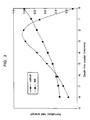
- Typical RF and optic field profiles for a Mach-Zehnder modulator of the design shown in Figs. 2 is shown in Fig. 3, which is a plot of field strength vs. distance (z-direction) showing the variation in RF and optic field strength and the overlap between in the active region of the modulator.
- Data points for the RF field curve are shown as squares and data points for the optic field profile are shown as circles. It is evident that the RF field peaks at the surface, as expected, while the peak for the optic field of the buried waveguide is 2-3 microns below the surface.
- the effectiveness of the electro-optic interaction can be improved if the peak in the RF profile more closely matches the peak in the optic profile.
- a device configuration is shown in Fig. 4.
- the lithium niobate substrate 41 is patterned to produce mesas with waveguides 42 buried in the mesas as shown. It will be recognized by those skilled in the art that the figures are not drawn to scale.
- the oxide buffer layer 45 in Fig. 4 is actually a thin deposited layer. In preferred structures the waveguide is located wholly or at least partially within the ridge.
- Fig. 4 The structure of Fig. 4 is relatively easy to fabricate by simply masking the waveguide regions and etching the surface of the lithium niobate substrate.
- the field profile for this device is shown in Fig. 5 and shows improved overlap between the RF and optical fields.
- the maxima of the two profiles are still separated in nearly the same way as with the device of Figs. 2 and 3.
- the peak in the RF field profile is shifted to below the nominal surface of the lithium niobate substrate.
- This is achieved with a structure represented by Fig. 6.
- the important and novel feature in this device structure is the formation of re-entrant sidewalls 55 on the mesas containing the waveguides 52.
- the peak in the RF field created by electrodes 53 and 54 is shifted closer to the peak in the optical profile thus optimizing the overlap and improving the effectiveness of the electro-optic interaction.
- the RF/optical field overlap can be improved, without degrading the capability for achieving a velocity matched device design, by altering the RF field distribution such that the peak in the RF field strength coincides with the peak in the optical field strength.
- One way to achieve this is to alter the radio-frequency relative permittivity of the crystal such that the relative dielectric constant of the optical waveguide has a minimal value at the point where the maximum RF field strength is desired. In this way a larger RF field can be produced in the region of the optical waveguide. This can be more clearly illustrated by analogy.
- the two materials are arranged within the capacitor gap in a sandwich configuration so that material "a” is confined to the very center of the gap region, and material “b” fills the rest of the gap on either side of material "a".
- the field distribution will be such that there will be a much larger field in the low dielectric material, material "a”. Stated another way, most of the voltage drop between the two capacitor plates will occur in the low dielectric material.
- This analogy can be applied to the optical modulator shown in Fig. 6. If the dielectric constant of the modulator is reduced only in the optical waveguide region, a larger RF field, and therefore a larger RF/optical overlap, will be achieved in the device.
- the effective dielectric constant of the ridge is dependent on the width of the ridge.
- the effective dielectric constant has a minimum at a point below the surface of the ridge.
- the RF field has a maximum near the center of the optical mode in the waveguide.
- the electrodes 54 are shown offset, i.e. recessed, in the z-direction due to the ridge structure.
- Devices with essentially equivalent performance, due to the re-entrant sidewall effect of the invention, can be produced with coplanar electrodes.
- structures with coplanar electrodes may be easier to process and package. It may be more apt to describe structures with coplanar electrodes as having waveguides bounded by "trenches", rather than as waveguides contained in "ridges".
- the relevant re-entrant sidewalls in such a case are the trench sidewalls. In much of the description herein these two cases are appropriately regarded as equivalent.
- RF and optical field profiles for the device of Fig. 6 are shown in Fig. 7.
- the maximum in the RF field profile has been shifted to below the surface of the ridge to a point that is approximately the peak in the optical field profile.
- a re-entrant sidewall i.e. a sidewall that is directed inwardly.
- the sidewall of the ridge will be sloped outwardly, or, if an ideal anisotropic etch is used, will be vertical.
- Specific and atypical process steps, which will be described below, are used to obtain a re-entrant sidewall. It is recommended that the re-entrant angle, i.e. the angle the sidewall makes with a vertical, is at least -5°, and preferably at least -10°, with more negative numbers meeting the prescribed conditions.
- the sidewalls are sloped uniformly.
- non-uniform slopes are also effective as long as the average width of the electrode gap at the bottom of the ridge is greater than the average width at the top of the ridge. This condition is met with continuous slopes or with stepped slopes. In either case the sidewall is considered re-entrant, i.e. essentially slopes inward.
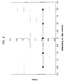
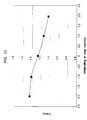
- Fig. 8 is a plot of effective overlap vs. extent of undercut for a device without a ridge, i.e. ridge height is zero and overlap is normalized at one. This curve is included as a baseline for Figs. 9-13.
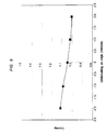
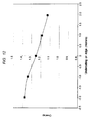
- the ridge width at the top of the ridge for the devices of Figs. 8-13 is 10 ⁇ m, the thickness of the electrode is 15 ⁇ m, and the gap distance between electrodes is 15 ⁇ m.
- Fig. 9 gives data points for a device with a 1 micron ridge.
- Fig. 10 gives data points for a 3 ⁇ m ridge height. Again moderate improvement is obtained with small undercuts but as the undercut increases the waveguide is perturbed and the effective overlap decreases.
- Fig. 11 shows data points for a 4 ⁇ m ridge height which, for the device geometry chosen for these models, gives optimum performance. As seen, a 44% improvement in overlap results with a 2 ⁇ m undercut. This compares with a device with a 4 ⁇ m ridge height with no undercut, i.e. 27%, resulting in an improvement of better than 60%.
- corresponding undercuts with deeper ridges actually produces diminishing returns in terms of overlap improvement.
- the device modeled in Fig. 12 has a ridge height of 5 ⁇ m
- the device modeled in Fig. 13 has a ridge height of 6 ⁇ m.
- improved overlap could be expected to occur in a variety of device geometries with ridge heights in the range 1-10 ⁇ m, and ridge widths in the range 3-20 ⁇ m.
- the range of suitable re-entrant angles is dependent on the starting geometry of the ridge and the size and location of the waveguide, but will typically be in the range -5° to -60°.
- a Mach-Zehnder device with lithium niobate substrate 60 is shown with electrodes 61 and waveguides 62.
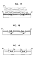
- a first ion implant represented by 63 in Fig. 15, is made at an angle with respect to the substrate as shown. The angle is approximately the desired re-entrant angle for the undercut structure of Fig. 6.
- the ion implant is used to selectively damage the lithium niobate crystal which then allows the damaged portions to be selectively etched with respect to the remainder of the substrate as is well known in the art.
- An implant of oxygen ions, with a dose of 5 x 10 14 /cm 3 or greater is suitable. Other ions such a He or H can be used.
- the implant can be made through the oxide buffer layer, however removal of the buffer layer is preferred which reduces the required implant energy.
- the result of the implant step is the formation of damaged regions 65, as shown in Fig. 16.
- a similar implant is then performed but with the complementary angle as represented by implant 67 in Fig. 17.
- the result of this second implant is the formation of damaged regions 68 shown in Fig. 18.
- the damaged regions 65 and 68 combine to form a total damaged area with a trapezoid shape.
- the damaged regions are then selectively etched using a wet etch of, e.g., ammonium hydroxide, hydrogen peroxide, and water, commonly referred to as an RCA solution, or 5% HF in water, or a 2:1 mixture of concentrated HNO 3 and HF.
- a photomask technique using multiple masks may also be used.
- An embodiment of this technique is shown in Figs. 20-24.
- a first mask 81 is applied to the substrate to mask the waveguide regions and define ridge regions.
- the mask material may be gold or tungsten, or other suitable material, that is patterned using standard lithographic techniques.
- a thick layer of photodefinable polymer, e.g. standard photoresist can be used which simplifies the process somewhat.
- the width of the portion of the mask overlying the waveguides is made wider than the waveguide as shown in Fig. 20.
- a first implant step is then performed, as shown in Fig. 21, with the energy of implant beam 85 adjusted for a relatively shallow implant 84, e.g.
- the energy of the ion implantation will depend on the geometry of the structure, etc. and energy/depth relationships are well known in the art.
- the depth of the second implant is preferably approximately equal to or greater than the depth of the waveguides.
- re-entrant sidewalls are somewhat stepped, as mentioned earlier, but are effective since the electrode gap width at the bottom of the trench is larger than the width of the trench above the bottom. It will be appreciated by those skilled in the art that the sequence of implant steps just described can be reversed and the same results obtained.
- the device is finished by depositing the buffer layer and forming the electrodes. It may be desirable to fill the trenches to give a planar structure. Techniques for filling trenches are well known and used in various forms of trench isolation, and in trench capacitors for MOS devices.
Landscapes
- Physics & Mathematics (AREA)
- Nonlinear Science (AREA)
- Electromagnetism (AREA)
- Chemical & Material Sciences (AREA)
- Engineering & Computer Science (AREA)
- Ceramic Engineering (AREA)
- Crystallography & Structural Chemistry (AREA)
- General Physics & Mathematics (AREA)
- Optics & Photonics (AREA)
- Optical Modulation, Optical Deflection, Nonlinear Optics, Optical Demodulation, Optical Logic Elements (AREA)
- Optical Integrated Circuits (AREA)
Abstract
Description
Claims (20)
- Electro-optic modulator comprising:the modulator characterized in that at least one of said sidewalls is re-entrant.(a) an electro-optic substrate, said substrate having a main surface portion and a raised surface portion, said raised surface portion comprising a ridge of electro-optic material extending along at least a portion of said main surface, said ridge having a ridge surface and ridge sidewalls,(b) an optical waveguide formed in said substrate with at least a portion thereof formed in said ridge,(c) a first electrode formed on said ridge surface,(d) at least one second electrode formed on said main surface portion,(e) means for impressing a voltage between said first and second electrodes,
- The electro-optic modulator of claim 1 wherein at least one of said sidewalls has a slope of at least -5° .
- The electro-optic modulator of claim 1 wherein the said electro-optic material is lithium niobate.
- The electro-optic modulator of claim 3 having electrodes on said main surface portion of said substrate and extending along both sidewalls of said ridge.
- The electro-optic modulator of claim 4 wherein both of the sidewalls are re-entrant.
- The electro-optic modulator of claim 5 wherein said ridge has a height in the range 1-10 µm.
- The electro-optic modulator of claim 6 wherein said ridge has a width in the range 3-20 µm.
- The electro-optic modulator of claim 1 wherein said waveguide splits into two Mach-Zehnder waveguide regions and recombines into a single waveguide.
- The electro-optic modulator of claim 8 wherein each of said Mach-Zehnder waveguide regions has a ridge as defined in claim 1.
- An electro-optic modulator comprising:(a) an electro-optic substrate,(b) a buried waveguide in said electro-optic substrate, said buried waveguide having two Mach-Zehnder portions essentially side by side, said Mach-Zehnder portions combining into a single input waveguide section and a single output waveguide section,(c) said Mach-Zehnder portions comprising:(i) a first trench extending along said substrate,(ii) a second trench extending along said substrate essentially parallel with said first trench and defining a ridge therebetween, said ridge having two ridge sidewalls and a ridge surface with at least one of said sidewalls being re-entrant, said ridge containing at least a portion of said waveguide, and(iii) an electrode on said ridge surface.
- The electro-optic modulator of claim 10 wherein at least one of said sidewalls has a slope in the range -5° to -60°.
- The electro-optic modulator of claim 11 wherein the said electro-optic material is lithium niobate.
- The electro-optic modulator of claim 12 having electrodes on said main surface portion of said substrate and extending along both sidewalls of said ridge.
- The electro-optic modulator of claim 12 wherein both of the sidewalls are re-entrant.
- The electro-optic modulator of claim 12 wherein said ridge has a height in the range 1-10 µm.
- The electro-optic modulator of claim 15 wherein said ridge has a width in the range 3-20 µm.
- A method for the manufacture of an electro-optic modulator comprising the steps of:(a) forming a buried waveguide in a substrate of electro-optic material,(b) depositing an electrode strip on said substrate overlying a portion of said buried waveguide, said portion defining a Mach-Zehnder electro-optic modulator region,(c) etching trenches in said substrate along each side of said buried waveguide in said Mach-Zehnder electro-optic modulator region to form a ridge of electro-optic material, with said waveguide at least partially contained in said ridge, said ridge of electro-optic material having at least one re-entrant sidewall.
- The method of claim 17 wherein said etching step is preceded by an ion implant step wherein a portion of said substrate corresponding to said trench is damaged by the ion implant step and the damage is created in the shape of a trapezoid to thereby create the said re-entrant sidewall.
- The method of claim 18 wherein said electrode is used as the implant mask during the ion implantation step.
- The method of claim 19 wherein the ion implant step comprises directing the ion beam on said substrate at a first angle, said angle corresponding approximately to the angle of said re-entrant sidewall, to form a first damaged region in said substrate, directing the ion beam on said substrate at a second angle to form a second damaged region in said substrate, said second angle being approximately the complement of said first angle, and etching away the first and second damaged regions to form a ridge with re-entrant sidewalls.
Applications Claiming Priority (2)
| Application Number | Priority Date | Filing Date | Title |
|---|---|---|---|
| US325870 | 1999-06-04 | ||
| US09/325,870 US6172791B1 (en) | 1999-06-04 | 1999-06-04 | Electro-optic modulators |
Publications (3)
| Publication Number | Publication Date |
|---|---|
| EP1058145A2 true EP1058145A2 (en) | 2000-12-06 |
| EP1058145A3 EP1058145A3 (en) | 2000-12-27 |
| EP1058145B1 EP1058145B1 (en) | 2004-03-31 |
Family
ID=23269818
Family Applications (1)
| Application Number | Title | Priority Date | Filing Date |
|---|---|---|---|
| EP00304335A Expired - Lifetime EP1058145B1 (en) | 1999-06-04 | 2000-05-23 | Electro-optic modulator and fabrication method thereof |
Country Status (4)
| Country | Link |
|---|---|
| US (1) | US6172791B1 (en) |
| EP (1) | EP1058145B1 (en) |
| JP (1) | JP3980250B2 (en) |
| DE (1) | DE60009385T2 (en) |
Cited By (2)
| Publication number | Priority date | Publication date | Assignee | Title |
|---|---|---|---|---|
| EP1289215A1 (en) * | 2001-08-21 | 2003-03-05 | Lucent Technologies Inc. | Optical MSK modulator |
| CN103852917A (en) * | 2012-11-30 | 2014-06-11 | 鸿富锦精密工业(深圳)有限公司 | electro-optic modulator |
Families Citing this family (29)
| Publication number | Priority date | Publication date | Assignee | Title |
|---|---|---|---|---|
| JP3954251B2 (en) * | 1999-08-27 | 2007-08-08 | 日本碍子株式会社 | Traveling waveform light modulator |
| JP4471520B2 (en) * | 2000-09-22 | 2010-06-02 | 日本碍子株式会社 | Traveling waveform light modulator |
| US6544431B2 (en) * | 2001-01-16 | 2003-04-08 | Triquint Technology Holding Co. | Thin film lithium niobate structure and method of making the same |
| US6846428B2 (en) | 2001-03-20 | 2005-01-25 | Wisconsin Alumni Research Foundation | Thin film lithium niobate and method of producing the same |
| US20020154843A1 (en) * | 2001-04-19 | 2002-10-24 | Betts Gary E. | Dielectric backfill for optical modulators using ridged substrates |
| US6853671B2 (en) * | 2001-06-13 | 2005-02-08 | Intel Corporation | Method and apparatus for tuning a laser with a Bragg grating in a semiconductor substrate |
| US7088877B2 (en) * | 2001-06-13 | 2006-08-08 | Intel Corporation | Method and apparatus for tuning a bragg grating in a semiconductor substrate |
| US6856732B2 (en) * | 2001-06-13 | 2005-02-15 | Intel Corporation | Method and apparatus for adding/droping optical signals in a semiconductor substrate |
| US20030015497A1 (en) * | 2001-07-18 | 2003-01-23 | Gill Douglas M. | Method of etching ferroelectric material |
| US6785430B2 (en) * | 2002-02-25 | 2004-08-31 | Intel Corporation | Method and apparatus for integrating an optical transmit module |
| US6951120B2 (en) * | 2002-03-19 | 2005-10-04 | Wisconsin Alumni Research Foundation | Machining of lithium niobate by laser ablation |
| US6950577B2 (en) * | 2002-07-01 | 2005-09-27 | Intel Corporation | Waveguide-based Bragg gratings with spectral sidelobe suppression and method thereof |
| US7245792B2 (en) * | 2002-08-16 | 2007-07-17 | Intel Corporation | Silicon-based tunable single passband optical filter |
| US6882757B2 (en) * | 2002-12-23 | 2005-04-19 | Agilent Technologies, Inc. | Velocity matched waveguide for traveling-wave optical modulators |
| JP4713866B2 (en) | 2004-09-14 | 2011-06-29 | 富士通オプティカルコンポーネンツ株式会社 | Optical device |
| US7397989B2 (en) * | 2004-09-21 | 2008-07-08 | Dynamic Method Enterprises Limited | Optical switches |
| US9164239B2 (en) * | 2006-03-15 | 2015-10-20 | Alcatel Lucent | Method and apparatus for optically filtering a communication signal |
| US8055141B2 (en) * | 2007-12-17 | 2011-11-08 | Alcatel Lucent | Balanced optical signal processor |
| JP5045821B2 (en) * | 2011-01-05 | 2012-10-10 | 富士通オプティカルコンポーネンツ株式会社 | Light modulator |
| TW201426151A (en) * | 2012-12-19 | 2014-07-01 | Hon Hai Prec Ind Co Ltd | Electro-optical modulator |
| WO2015030891A2 (en) * | 2013-06-03 | 2015-03-05 | Massachusetts Institute Of Technology | Inductance-tuned electro-optic modulators |
| US11137536B2 (en) | 2018-07-26 | 2021-10-05 | Facebook Technologies, Llc | Bragg-like gratings on high refractive index material |
| US11016360B1 (en) | 2019-05-07 | 2021-05-25 | Massachusetts Institute Of Technology | Optical modulator RF electrodes |
| US12601938B2 (en) * | 2019-11-27 | 2026-04-14 | HyperLight Corporation | Electro-optic devices having closely spaced engineered electrodes |
| JP7701354B2 (en) | 2019-11-27 | 2025-07-01 | ハイパーライト・コーポレーション | Electro-optical device having improved electrodes |
| US12656637B1 (en) | 2019-11-27 | 2026-06-16 | HyperLight Corporation | Lithium niobate photonic devices having engineered lithium niobate, silicon dioxide, and electrode extension thickness |
| US11226446B2 (en) | 2020-05-06 | 2022-01-18 | Facebook Technologies, Llc | Hydrogen/nitrogen doping and chemically assisted etching of high refractive index gratings |
| CN115885208A (en) | 2020-06-02 | 2023-03-31 | 超光公司 | High Performance Optical Modulators and Drivers |
| US20250053064A1 (en) * | 2023-08-11 | 2025-02-13 | Taiwan Semiconductor Manufacturing Co., Ltd. | Optical devices and methods of manufacture |
Family Cites Families (8)
| Publication number | Priority date | Publication date | Assignee | Title |
|---|---|---|---|---|
| JP2928532B2 (en) * | 1988-05-06 | 1999-08-03 | 株式会社日立製作所 | Quantum interference optical device |
| US5347601A (en) * | 1993-03-29 | 1994-09-13 | United Technologies Corporation | Integrated optical receiver/transmitter |
| JP3573476B2 (en) * | 1993-12-10 | 2004-10-06 | 富士写真フイルム株式会社 | Optical element |
| KR100357787B1 (en) * | 1994-01-31 | 2003-01-24 | 가부시끼가이샤 히다치 세이사꾸쇼 | Manufacturing method of waveguide fluorescent element |
| JPH08116124A (en) * | 1994-10-13 | 1996-05-07 | Hitachi Ltd | Semiconductor optical device |
| US5790719A (en) * | 1995-11-28 | 1998-08-04 | Nippon Telegraph And Telephone Corporation | Optical control device |
| US5781327A (en) * | 1996-08-19 | 1998-07-14 | Trw Inc. | Optically efficient high dynamic range electro-optic modulator |
| JPH11202274A (en) * | 1998-01-07 | 1999-07-30 | Oki Electric Ind Co Ltd | Ridge waveguide type semiconductor optical functional device and method of manufacturing the same |
-
1999
- 1999-06-04 US US09/325,870 patent/US6172791B1/en not_active Expired - Lifetime
-
2000
- 2000-05-23 DE DE60009385T patent/DE60009385T2/en not_active Expired - Lifetime
- 2000-05-23 EP EP00304335A patent/EP1058145B1/en not_active Expired - Lifetime
- 2000-06-05 JP JP2000166997A patent/JP3980250B2/en not_active Expired - Fee Related
Cited By (3)
| Publication number | Priority date | Publication date | Assignee | Title |
|---|---|---|---|---|
| EP1289215A1 (en) * | 2001-08-21 | 2003-03-05 | Lucent Technologies Inc. | Optical MSK modulator |
| CN103852917A (en) * | 2012-11-30 | 2014-06-11 | 鸿富锦精密工业(深圳)有限公司 | electro-optic modulator |
| CN103852917B (en) * | 2012-11-30 | 2018-10-26 | 陈伟民 | electro-optic modulator |
Also Published As
| Publication number | Publication date |
|---|---|
| EP1058145A3 (en) | 2000-12-27 |
| EP1058145B1 (en) | 2004-03-31 |
| JP2001004966A (en) | 2001-01-12 |
| DE60009385T2 (en) | 2005-03-24 |
| DE60009385D1 (en) | 2004-05-06 |
| JP3980250B2 (en) | 2007-09-26 |
| US6172791B1 (en) | 2001-01-09 |
Similar Documents
| Publication | Publication Date | Title |
|---|---|---|
| EP1058145B1 (en) | Electro-optic modulator and fabrication method thereof | |
| EP3794409B1 (en) | Integration of photonic components on soi platform | |
| US7005247B1 (en) | Controlled selectivity etch for use with optical component fabrication | |
| CN112436381B (en) | High-speed DFB laser chip and manufacturing method thereof | |
| US8377320B2 (en) | Method of forming an undercut microstructure | |
| WO2019220207A1 (en) | lll-V/SI HYBRID OPTOELECTRONIC DEVICE AND METHOD OF MANUFACTURE | |
| US20260056363A1 (en) | External layer waveguiding in thin film lithium-containing photonic devices | |
| JPH07112100B2 (en) | Optoelectronic semiconductor device and manufacturing method thereof | |
| KR100226736B1 (en) | Isolation Area Formation Method | |
| JP2010096958A (en) | Optical modulator | |
| US4851079A (en) | Producing lithium niobate waveguide structures | |
| KR100427581B1 (en) | Method for manufacturing semiconductor optical device | |
| CN115857200B (en) | Electro-optic modulator and method of making same | |
| CN116263521B (en) | Photodetector integrated with an anti-cone shape including a curved end | |
| CN114336275B (en) | Manufacturing method of electrode contact window and preparation method of semiconductor device | |
| JP3572713B2 (en) | Method for manufacturing semiconductor quantum wire device | |
| WO2004008203A1 (en) | Planar waveguide with tapered region | |
| WO2001026193A1 (en) | Method for making a ridge waveguide semiconductor device | |
| CN121172562B (en) | A germanium-filled double-groove high-reflectivity surface grating structure and its fabrication method | |
| CN222259620U (en) | Selective epitaxial silicon-based ridge optical waveguide | |
| CN116626922B (en) | Preparation method of built-in electrode type thin film lithium niobate electro-optical modulator | |
| TWI918456B (en) | Electroabsorption modulator | |
| JP2014160131A (en) | Optical modulator | |
| JP2005520328A (en) | Method for manufacturing optical communication device and optical communication device | |
| CN121348597A (en) | Patterning methods and semiconductor devices |
Legal Events
| Date | Code | Title | Description |
|---|---|---|---|
| PUAI | Public reference made under article 153(3) epc to a published international application that has entered the european phase |
Free format text: ORIGINAL CODE: 0009012 |
|
| PUAL | Search report despatched |
Free format text: ORIGINAL CODE: 0009013 |
|
| AK | Designated contracting states |
Kind code of ref document: A2 Designated state(s): AT BE CH CY DE DK ES FI FR GB GR IE IT LI LU MC NL PT SE |
|
| AX | Request for extension of the european patent |
Free format text: AL;LT;LV;MK;RO;SI |
|
| AK | Designated contracting states |
Kind code of ref document: A3 Designated state(s): AT BE CH CY DE DK ES FI FR GB GR IE IT LI LU MC NL PT SE |
|
| AX | Request for extension of the european patent |
Free format text: AL;LT;LV;MK;RO;SI |
|
| RAP1 | Party data changed (applicant data changed or rights of an application transferred) |
Owner name: AGERE SYSTEMS OPTOELECTRONICS GUARDIAN CORPORATION |
|
| AKX | Designation fees paid | ||
| RBV | Designated contracting states (corrected) |
Designated state(s): DE FR GB |
|
| 17P | Request for examination filed |
Effective date: 20010723 |
|
| GRAP | Despatch of communication of intention to grant a patent |
Free format text: ORIGINAL CODE: EPIDOSNIGR1 |
|
| RIC1 | Information provided on ipc code assigned before grant |
Ipc: 7G 02F 1/035 A Ipc: 7G 02B 6/12 B Ipc: 7G 02F 1/225 B |
|
| RTI1 | Title (correction) |
Free format text: ELECTRO-OPTIC MODULATOR AND FABRICATION METHOD THEREOF |
|
| RIC1 | Information provided on ipc code assigned before grant |
Ipc: 7G 02F 1/035 A Ipc: 7G 02F 1/225 B Ipc: 7G 02B 6/12 B |
|
| RTI1 | Title (correction) |
Free format text: ELECTRO-OPTIC MODULATOR AND FABRICATION METHOD THEREOF |
|
| GRAS | Grant fee paid |
Free format text: ORIGINAL CODE: EPIDOSNIGR3 |
|
| GRAA | (expected) grant |
Free format text: ORIGINAL CODE: 0009210 |
|
| AK | Designated contracting states |
Kind code of ref document: B1 Designated state(s): DE FR GB |
|
| REG | Reference to a national code |
Ref country code: GB Ref legal event code: FG4D |
|
| REF | Corresponds to: |
Ref document number: 60009385 Country of ref document: DE Date of ref document: 20040506 Kind code of ref document: P |
|
| ET | Fr: translation filed | ||
| PLBE | No opposition filed within time limit |
Free format text: ORIGINAL CODE: 0009261 |
|
| STAA | Information on the status of an ep patent application or granted ep patent |
Free format text: STATUS: NO OPPOSITION FILED WITHIN TIME LIMIT |
|
| 26N | No opposition filed |
Effective date: 20050104 |
|
| PGFP | Annual fee paid to national office [announced via postgrant information from national office to epo] |
Ref country code: GB Payment date: 20140521 Year of fee payment: 15 |
|
| PGFP | Annual fee paid to national office [announced via postgrant information from national office to epo] |
Ref country code: FR Payment date: 20140509 Year of fee payment: 15 Ref country code: DE Payment date: 20140521 Year of fee payment: 15 |
|
| REG | Reference to a national code |
Ref country code: DE Ref legal event code: R119 Ref document number: 60009385 Country of ref document: DE |
|
| GBPC | Gb: european patent ceased through non-payment of renewal fee |
Effective date: 20150523 |
|
| REG | Reference to a national code |
Ref country code: FR Ref legal event code: ST Effective date: 20160129 |
|
| PG25 | Lapsed in a contracting state [announced via postgrant information from national office to epo] |
Ref country code: DE Free format text: LAPSE BECAUSE OF NON-PAYMENT OF DUE FEES Effective date: 20151201 Ref country code: GB Free format text: LAPSE BECAUSE OF NON-PAYMENT OF DUE FEES Effective date: 20150523 |
|
| PG25 | Lapsed in a contracting state [announced via postgrant information from national office to epo] |
Ref country code: FR Free format text: LAPSE BECAUSE OF NON-PAYMENT OF DUE FEES Effective date: 20150601 |