EP1057094B1 - Circuit integre intelligent - Google Patents
Circuit integre intelligent Download PDFInfo
- Publication number
- EP1057094B1 EP1057094B1 EP99961162A EP99961162A EP1057094B1 EP 1057094 B1 EP1057094 B1 EP 1057094B1 EP 99961162 A EP99961162 A EP 99961162A EP 99961162 A EP99961162 A EP 99961162A EP 1057094 B1 EP1057094 B1 EP 1057094B1
- Authority
- EP
- European Patent Office
- Prior art keywords
- processor
- main
- integrated circuit
- intelligent integrated
- circuit according
- Prior art date
- Legal status (The legal status is an assumption and is not a legal conclusion. Google has not performed a legal analysis and makes no representation as to the accuracy of the status listed.)
- Expired - Lifetime
Links
Images




Classifications
-
- G—PHYSICS
- G07—CHECKING-DEVICES
- G07F—COIN-FREED OR LIKE APPARATUS
- G07F7/00—Mechanisms actuated by objects other than coins to free or to actuate vending, hiring, coin or paper currency dispensing or refunding apparatus
- G07F7/08—Mechanisms actuated by objects other than coins to free or to actuate vending, hiring, coin or paper currency dispensing or refunding apparatus by coded identity card or credit card or other personal identification means
- G07F7/10—Mechanisms actuated by objects other than coins to free or to actuate vending, hiring, coin or paper currency dispensing or refunding apparatus by coded identity card or credit card or other personal identification means together with a coded signal, e.g. in the form of personal identification information, like personal identification number [PIN] or biometric data
- G07F7/1008—Active credit-cards provided with means to personalise their use, e.g. with PIN-introduction/comparison system
-
- G—PHYSICS
- G06—COMPUTING OR CALCULATING; COUNTING
- G06F—ELECTRIC DIGITAL DATA PROCESSING
- G06F21/00—Security arrangements for protecting computers, components thereof, programs or data against unauthorised activity
- G06F21/70—Protecting specific internal or peripheral components, in which the protection of a component leads to protection of the entire computer
- G06F21/71—Protecting specific internal or peripheral components, in which the protection of a component leads to protection of the entire computer to assure secure computing or processing of information
- G06F21/75—Protecting specific internal or peripheral components, in which the protection of a component leads to protection of the entire computer to assure secure computing or processing of information by inhibiting the analysis of circuitry or operation
- G06F21/755—Protecting specific internal or peripheral components, in which the protection of a component leads to protection of the entire computer to assure secure computing or processing of information by inhibiting the analysis of circuitry or operation with measures against power attack
-
- G—PHYSICS
- G06—COMPUTING OR CALCULATING; COUNTING
- G06F—ELECTRIC DIGITAL DATA PROCESSING
- G06F21/00—Security arrangements for protecting computers, components thereof, programs or data against unauthorised activity
- G06F21/70—Protecting specific internal or peripheral components, in which the protection of a component leads to protection of the entire computer
- G06F21/71—Protecting specific internal or peripheral components, in which the protection of a component leads to protection of the entire computer to assure secure computing or processing of information
- G06F21/77—Protecting specific internal or peripheral components, in which the protection of a component leads to protection of the entire computer to assure secure computing or processing of information in smart cards
-
- G—PHYSICS
- G06—COMPUTING OR CALCULATING; COUNTING
- G06F—ELECTRIC DIGITAL DATA PROCESSING
- G06F21/00—Security arrangements for protecting computers, components thereof, programs or data against unauthorised activity
- G06F21/70—Protecting specific internal or peripheral components, in which the protection of a component leads to protection of the entire computer
- G06F21/81—Protecting specific internal or peripheral components, in which the protection of a component leads to protection of the entire computer by operating on the power supply, e.g. enabling or disabling power-on, sleep or resume operations
-
- G—PHYSICS
- G06—COMPUTING OR CALCULATING; COUNTING
- G06F—ELECTRIC DIGITAL DATA PROCESSING
- G06F9/00—Arrangements for program control, e.g. control units
- G06F9/06—Arrangements for program control, e.g. control units using stored programs, i.e. using an internal store of processing equipment to receive or retain programs
- G06F9/30—Arrangements for executing machine instructions, e.g. instruction decode
- G06F9/38—Concurrent instruction execution, e.g. pipeline or look ahead
- G06F9/3877—Concurrent instruction execution, e.g. pipeline or look ahead using a secondary processor, e.g. coprocessor
- G06F9/3879—Concurrent instruction execution, e.g. pipeline or look ahead using a secondary processor, e.g. coprocessor for non-native instruction execution, e.g. executing a command; for Java instruction set
-
- G—PHYSICS
- G06—COMPUTING OR CALCULATING; COUNTING
- G06F—ELECTRIC DIGITAL DATA PROCESSING
- G06F9/00—Arrangements for program control, e.g. control units
- G06F9/06—Arrangements for program control, e.g. control units using stored programs, i.e. using an internal store of processing equipment to receive or retain programs
- G06F9/46—Multiprogramming arrangements
- G06F9/54—Interprogram communication
- G06F9/541—Interprogram communication via adapters, e.g. between incompatible applications
-
- G—PHYSICS
- G06—COMPUTING OR CALCULATING; COUNTING
- G06Q—INFORMATION AND COMMUNICATION TECHNOLOGY [ICT] SPECIALLY ADAPTED FOR ADMINISTRATIVE, COMMERCIAL, FINANCIAL, MANAGERIAL OR SUPERVISORY PURPOSES; SYSTEMS OR METHODS SPECIALLY ADAPTED FOR ADMINISTRATIVE, COMMERCIAL, FINANCIAL, MANAGERIAL OR SUPERVISORY PURPOSES, NOT OTHERWISE PROVIDED FOR
- G06Q20/00—Payment architectures, schemes or protocols
- G06Q20/30—Payment architectures, schemes or protocols characterised by the use of specific devices or networks
- G06Q20/34—Payment architectures, schemes or protocols characterised by the use of specific devices or networks using cards, e.g. integrated circuit [IC] cards or magnetic cards
- G06Q20/341—Active cards, i.e. cards including their own processing means, e.g. including an IC or chip
-
- G—PHYSICS
- G07—CHECKING-DEVICES
- G07F—COIN-FREED OR LIKE APPARATUS
- G07F7/00—Mechanisms actuated by objects other than coins to free or to actuate vending, hiring, coin or paper currency dispensing or refunding apparatus
- G07F7/08—Mechanisms actuated by objects other than coins to free or to actuate vending, hiring, coin or paper currency dispensing or refunding apparatus by coded identity card or credit card or other personal identification means
- G07F7/0806—Details of the card
- G07F7/0813—Specific details related to card security
- G07F7/082—Features insuring the integrity of the data on or in the card
-
- G—PHYSICS
- G06—COMPUTING OR CALCULATING; COUNTING
- G06F—ELECTRIC DIGITAL DATA PROCESSING
- G06F2207/00—Indexing scheme relating to methods or arrangements for processing data by operating upon the order or content of the data handled
- G06F2207/72—Indexing scheme relating to groups G06F7/72 - G06F7/729
- G06F2207/7219—Countermeasures against side channel or fault attacks
Definitions
- microprocessors or microcomputers or intelligent integrated circuits sequentially execute instructions from a program saved in a memory, in synchronism with one or several timing signals referenced with respect to signals clock supplied to microprocessor or microcomputer or circuit integrated either internally or externally.
- intelligent integrated circuit we includes an integrated circuit with specific circuits and limited to the execution of a limited number of instructions or functionalities for which they have been specifically developed.
- a given action could be produce at different times depending on the result of an operation determined security, such as testing confidential internal information or the decryption of a message, or the integrity check of certain information.
- an operation determined security such as testing confidential internal information or the decryption of a message, or the integrity check of certain information.
- MUMIC Multi Untraceable MICrocomputer
- the intelligent integrated circuit has a main processor and an operating system running a program main to constitute a main process carrying out tasks, at least a secondary processor capable of running at least one secondary program to constitute at least one process carrying out tasks, characterized in that it comprises common supply circuits between the processors and means of ensuring that the secondary energy process (es) similar and with a different operating signature, are performed concurrently with the main process by inducing in circuits feeding, continuously or intermittently, disturbances energy, related to the tasks executed by the secondary process or processes, which are superimposed on the energy consumption generated by the execution of the tasks of the main process to carry out continuous or intermittent interference, sequencing the main process.
- the secondary energy process es
- WO-A-97/04376 is a state of the art representing the preamble of claim 1.
- the main processors or secondary are each a secure microprocessor or microcomputer.
- the activation of these means is triggered by the operating system of the main processor (1) of the integrated circuit intelligent, so that the additional security created by the means above depends only on a decision resulting from the execution by the main operating system processor located in a circuit location integrated inaccessible from the outside.
- the intelligent integrated circuit has a main memory, dedicated to the main processor, containing the system operating in at least part of it inaccessible from the outside and accessible by at least one of the two processors and a secondary memory respectively dedicated to the secondary processor.
- the intelligent integrated circuit has at minus a communication bus between the processors, their memories and an input output circuit.
- the intelligent integrated circuit is produced at using logic circuits dispersed on the substrate (s) so that the physical implantation of the two processors is carried out without blocks easily identifiable functional, for example by physical nesting but with a separate logical organization.
- the secondary processor performs secondary process tasks that minimize or cancel signatures of main processor operation.
- the secondary processor performs tasks of the secondary process correlated to those of the main process executed by the main processor in such a way that the results processing intermediates never appear during the process.
- the secondary program uses a smaller workspace than the main program.
- a second object of the invention is to ensure that the process main can only work if the secondary process is operational.
- This second goal is achieved by the fact that the intelligent integrated circuit has means of communication between the main processor and the secondary processor.
- the means of communication between the two processors let the main processor know if the processor secondary is operational or not.
- the means of communication between the two processors allow the main processor to perform a secondary processor authentication.
- the authentication test or secondary processor operation is performed during processing by the main processor.
- the processor activation means secondary is controlled either by the main processor and its program main, either by an interrupt system, or by a time counter, or again by a combination of the three
- a third object of the invention is to ensure that the process secondary implements a program that is totally different from main program.
- This third goal is achieved by the fact that the secondary processor performs tasks of the secondary process without correlation with those of the main process executed by the main processor.
- the secondary processor performs secondary process tasks that minimize or cancel signatures of main processor operation.
- a fourth object of the invention is that the secondary program uses a program whose signature induces effects opposite to those emanating from the main processor.
- This fourth goal is achieved by the fact that the secondary program implements a process correlated to the main process, so that the combination of the two processes provides an operating signature of the secondary processor which hides that of the main processor.
- the secondary processor performs tasks correlated to those of the main processor in such a way that the intermediate results of treatment never appear during the process.
- a fifth object of the invention is to provide an architecture original using validated circuits, without the need to create a new semiconductor technology or new processes for manufacturing.
- This fifth goal is achieved by the fact that the secondary processor can replace the main processor and vice versa.
- the secondary processor performs tasks correlated to those of the main processor by synchronization of process and compare values of two data each from the respective processor executing its respective program.
- the secondary processor performs tasks correlated to those of the main processor by logical deduction of the secondary program from the main program.
- the intelligent integrated circuit comprises at at least two processors and each of the processors has a respective bus to which the random access memories, read only memories for each processor and non-volatile for the main processor.
- the intelligent integrated circuit includes a plurality of processors each of which is connected to a single bus multiplexed communication between processors and a set of memory alive, dead and non-volatile connected to this bus, conflicts of access to this common bus being managed by an arbitration circuit.
- the secondary processor executes successively and in any order, either correlated programs, either programs without correlation with those executed by the processor main.
- the intelligent integrated circuit object of the invention is called MUMIC (Multi Untraceable MICrocomputer) and a first variant of its constitution logic will be explained in connection with Figure 1.
- This logical constitution is not representative of the physical constitution or implantation topological, as we will see later.
- This intelligent integrated circuit is consisting of a main processor (1) and a secondary processor (2), each processor being connected by its communication bus (Addresses, Data and commands) respective (3,4) to memories respective (12,13,22) containing the main program (P1) and the program secondary (P2) to be executed by each of the respective main processors (1) and secondary (2), and work registers, such as, for example, volatile RAM memories (11,21).
- the memories linked to the processor secondary are "trompe l'oeil" memories (DumRAM 21) and dead (DumROM 22) which allow the secondary processor (2) to execute tasks overlapping those of the main processor (1).
- the system main processor is, for example, contained in a part inaccessible from outside the ROM (12), but accessible by at least one of the two processors.
- Each processor (1, 2) has its own own sequencer (19, respectively 20).
- the integrated circuit according to the invention also includes an input-output circuit (14) connected, on the one hand to the bus single or main processor bus when the circuit is made according to a variant with several buses and on the other hand, for example by contacts or a contactless connection device to the outside world to receive signals of a terminal.
- a set of registers (R1, R2, R3) and an interrupt circuit (15) can be added to the processor which needs it for the implementation work of one of the operating variants corresponding to a variant of realization described below.
- the three elements (R1, R2, R3) are linked to a interrupt generation circuit (15) which is connected to the inputs processor interruption (in this case the main one).
- the operating system of the main processor (1) is unique in the case of a main processor variant slave secondary processor and is located in the read-only memory (12) accessible by the processor main.
- a second operating system or the same operating system can be made accessible to the processor secondary, for example by an access right token exchange and a control of this access right before the processor hands over to the other.
- an interrupt circuit can be added to each processor which needs for the role it should play, especially in the case of the exchange of role or in the variant embodiment of FIG. 2a.
- the main program (P1) is contained in the non-volatile memory (13) and the use of trompe-l'oeil memories corresponds to that described in French patent application published under number FR 2 765 361, corresponding to European application EP-A-0 920 660, taking account of the fact that there can be simultaneity of execution between at least two intelligent integrated circuit processors. In such a case, the two types of memories (trompe l'oeil and the others) are exploited during the same periods, even if the bus is actually multiplexed.
- Application EP-A-0 920 660 constitutes a state of the art according to Article 54 (3) EPC.
- the integrated circuit also includes an input-output interface connected to at least one bus of the integrated circuit, this interface possibly being of the type either parallel / parallel, or parallel / series.
- the main RAM (1) RAM working memory (11) can be merged with the processor trompe-l'oeil RAM (21 DumRAM) secondary (2) to form a single dual port memory as shown in Figure 5.
- These dual-port memories, bright (11-21)) use a pair of address registers (110, 210), for receiving address signals (ADDO, ADD1) and allow access by the main processor (1), respectively secondary (2).
- These dual-port memories, bright (11-21) also use a first pair (111, 211) of data registers to allow data read access by the main processor (1), respectively secondary (2).
- the outputs of the read data registers are connected to amplifiers (113, 213) which deliver the signals of data (D0, D1). Finally these dual port memories, vivid (11-21) use also a second pair (112, 212) of data registers for allow write access to data by the main processor (1), respectively secondary (2).
- This type of dual port memory architecture is available from suppliers such as Motorola or Texas Instrument.
- the dual port memories synchronous or asynchronous, allow access, by two distinct channels, to a memory address zone, in reading or in writing. They are used, in particular, to regulate synchronization between separate systems.
- the use of dual memory ports for synchronizing processes is based on the fact that processors can access the memory by two independent channels (address and data) synchronously or asynchronously and share data that can be used simultaneously.
- the two processors (1,2), their bus (3,4) and their memories (11,21; 12,13,22) are supplied by common supply circuits (6) of so as to minimize the distinction between one's energy calls or the other processor.
- common supply circuits (6) of so as to minimize the distinction between one's energy calls or the other processor.
- RAM random access memories
- dead ROM (12 and 22)
- NVM programmable non-volatile (13)
- a feature of the invention resides in the fact that the logical, arithmetic operators, as well as control functions would be mixed, at the level of the doors or elementary cells, with each other so that we cannot a priori determine the physical location of a cell belonging to a function. So each processor would be broken up into a number of elements represented by squares or rectangles on Figure 6.
- the two processors (1,2) can be physically nested, despite logical organization separated, so much so that two adjacent transistors can either belong to one, either to the other processors or their associated circuits.
- This is returned possible by the fact that the circuit class to which the domain of microprocessor card does not impose high performance in terms of clock cycle.
- This mode of setting up circuits is therefore particularly favorable to ensuring the security of the whole.
- the realization of such circuits require computer-assisted automatic tracing to ensure correct signal routing and control of functionality. We design so that the consumption of each functional block is perfectly nested and combine completely.
- the two processors can communicate, either by through a specific link, either by a set (50, 51, FIG. 2a) of communication registers connected to the buses (3,4), or again by theft of cycle on the bus of the other processor, or again by an arbitration logic, in the case of a bus shared between the two processors, as shown figure 3.
- Figure 2a shows, for example, a link using two registers (50,51) operating in interrupt mode using the circuits of detection (B1, B2), but we can also use a dual access register (5) with a protocol similar to that used in smart cards, that is to say in which the main processor (1) is the master.
- a first register (50) provides the connection between the bus (3) of the main processor (1) and that (4) of the secondary processor (2), while a second register (51) provides the link in the other direction.
- Each of the first (50), respectively second (51), registers is provided with a first rocker (B1), respectively second flip-flop (B2), of storage which passes to the state active when information has been posted in the corresponding register.
- FIG. 2b represents the structure of a frame with a header, a data field and a field for detecting errors.
- Each frame can constitute either an information block (block I) or a block of acknowledgment (block A), each of these blocks being able to be transmitted in the both directions.
- the header can consist of two bytes, the first giving the block number and the second the length.
- the flip-flop When a block is posted in the first register (50), the flip-flop produces a signal which is interpreted as a IT1 interruption by the secondary processor (2), thus allowing it to be warned that a message to its destination is present in the first register (50).
- the secondary processor (2) can therefore grasp the block by reading the content of the first register (50), then acknowledge receipt of the block by a block of acknowledgment (block A) posted in the second register (51) to the main processor (1) with the same number.
- This process is known for allow in particular the chaining of blocks, although this is not absolutely necessary in the context of this invention.
- the information field can itself be divided into two parts: a command field and a data field. The field of command thus allows the main processor to send instructions to the secondary processor.
- the two programs (P1, P2) run respectively in the main (1) and secondary (2) processor so that two instructions run simultaneously. It is also possible to shift the phases of the clock driving the secondary processor (2) so that the cycles instructions do not exactly match in each of processors.
- the offsets can also be made variable and random, which will result in superimposed instruction cycles also variable. These shifts can be generated by the sequencer (20) of the secondary processor (2).
- the secondary processor (2) can be left running permanently, but it is better to have a communication channel between the two processors which can be advantageously used to activate the secondary processor (2) and / or to signal to the main processor (1) that the secondary processor (2) is operational and / or actually performs tasks.
- Processors have at least two states: active or inactive.
- the active state corresponds to the execution of a series of various operations and the inactive state can be achieved by a waiting loop containing no surgery.
- the passage from one state to another is carried out by a mechanism of communication between processors.
- the main processor can activate an idle secondary processor by sending an interrupt to this one.
- the processors each have either an interrupt line at destination of at least one other processor, ie a reset line.
- the authentication mechanism is triggered at the request of the processor main (1), or periodically, or even randomly. As soon as the main processor (1) detects an anomaly during authentication, it can stop any treatment, or put itself in a waiting loop.
- an operation of this type can be used in interruption.
- a dialogue begins between the two processors to perform processor-driven authentication main (1).
- This authentication consists, for example, in encrypting by the main processor (1) data based on a key stored in a secret zone of a connected non-volatile programmable memory (13, NVM) to the bus (3) of the main processor (1).
- the encrypted data is sent to secondary processor (2) via the communication channel and the latter decrypts then returns the result to the main processor (1) which compares the result of data decryption. If the result is correct, the processor principal (1) can continue working, otherwise he enters a waiting loop pending the next authentication.
- the main processor (1) can also come and test an activity register in the secondary memory "trompe-l'oeil" (DumRAM, 22) of the secondary processor (2) and note that this register is indeed modified at each test. If this register is not modified, the main processor can suspend its activity so similar to the previous one.
- the secondary processor (2) can also be executed with a program correlated to that which is executed by the main processor so such that the intermediate treatment results never appear at the during execution.
- a program correlated to that which is executed by the main processor so such that the intermediate treatment results never appear at the during execution.
- fault-intolerant programs ie capable of detect faults
- CPU processors
- Exchange and comparison operations can be carried out, either in software (similar to the sequence of instructions 6 - 6 "described above), either in material by a comparator (8) such as that of FIG. 4 which is activated by a signal resulting from the synchronization operation and delivered on its validation input (80).
- the comparator (8) also receives on its other inputs (81, 82) the signals representative of the values of the counters ordinal (PC, PC ') respective to each main (1) and secondary processor (2).
- the hardware comparator (8) will trigger by the signal (attack interrupt) emitted on its output (83), the processing of an interrupt then performing the appropriate operations through the mechanism microprocessor interruption (example: Reset interrupt).
- the main processor (1) activates a timer (R3) initialized either using the random generator (R1), either from the content of the programmable non-volatile memory (13, NVM).
- This programmable non-volatile memory (13) can indeed contain a unique number changed with each use.
- the time counter (R3) expires after an unpredictable time from the outside, it triggers an authentication of the secondary processor (2) by the main processor (1).
- the register (R2) can, after having been loaded with specific information (e.g. from a memory or random generator (R1)), be used to trigger a interruption.
- specific information e.g. from a memory or random generator (R1)
- a random generator (R1) is connected to the interrupt system (15) of the main microprocessor (1) so as to cause irregular and completely desynchronized interruptions by report on the execution of programs in the main processor (1).
- the interrupt system can be maskable or not depending on the treatment considered. In this case, if the interruption is hidden, the operation of the assembly is conventional in monoprocessor, but as soon as the main program (P1) in progress wants to protect itself against possible observations, it authorizes this interrupt which triggers authentication and activation of the secondary processor (2).
- each processor (1a, 1b, ..., 1n, fig.3) is connected to a centralized arbitration logic (8) by three types of lines, a first bus request (31) (Bus Request), a second busy bus (32) (Bus Busy) and a third bus scan (33) (Bus Polling) of the bus common (3).
- the first two types, request (31) and busy (32) are consisting respectively of a single line common to all the processors, while the last type, polling (33) is an individual line (33a, 33b, ..., 33n) to each of the n processors (1a, 1b, ..., 1n). All of the processors share random access memory (RAM) through the single bus (3), read only memory (ROM), programmable non-volatile memory (NVM) and input output circuit (I / O).
- RAM random access memory
- ROM read only memory
- NVM programmable non-volatile memory
- I / O input output circuit
- a processor (for example, 1a) wishing to acquire the bus (3) indicates this wish on the bus request line (31).
- the referee (8) questions the others processors (1b, ..., 1n) according to a well-defined algorithm (example: cyclic interrogation, bus scan) on scan type lines (33b, ..., 33n) corresponding to the processors questioned.
- the arbitrator (8) does not resume the questioning until the bus (3) released by the passage of the signal transmitted on the busy bus line (32) of active state to inactive state.
- the processors are connected on a single bus, which they share access to multiplexing these accesses over time.
- the interference produced by the invention can be made intermittent by using intermittent operation monoprocessor, for example, to deliver results to the outside world, for testing purposes, or hide the time counter interrupts (R3) or the random generator.
- the main program (P1) authorizes the operation of the processor secondary (2) in order to "scramble" the operation.
- the two processors can alternately play the role of main processor and secondary processor. This assumes that a token of priority be exchanged between the two processors to give that of the two who holds him the role of master at a given time.
Landscapes
- Engineering & Computer Science (AREA)
- Theoretical Computer Science (AREA)
- Physics & Mathematics (AREA)
- Software Systems (AREA)
- General Physics & Mathematics (AREA)
- Computer Hardware Design (AREA)
- Computer Security & Cryptography (AREA)
- General Engineering & Computer Science (AREA)
- Mathematical Physics (AREA)
- Business, Economics & Management (AREA)
- Computer Networks & Wireless Communication (AREA)
- Microelectronics & Electronic Packaging (AREA)
- Accounting & Taxation (AREA)
- Strategic Management (AREA)
- General Business, Economics & Management (AREA)
- Multi Processors (AREA)
- Microcomputers (AREA)
- Storage Device Security (AREA)
- Power Sources (AREA)
- Semiconductor Integrated Circuits (AREA)
- Input Circuits Of Receivers And Coupling Of Receivers And Audio Equipment (AREA)
- Electronic Switches (AREA)
Description
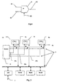
- la figure 1 représente un schéma logique d'un mode de réalisation du circuit intégré de l'invention à deux processeurs avec chacun leur bus ;
- la figure 2a représente un exemple de réalisation d'un circuit de communication entre deux processeurs du circuit ;
- la figure 2b représente la structure d'une trame utilisée dans la communication entre les deux processeurs du circuit ;
- la figure 3 représente un schéma d'un mode de réalisation du circuit intégré de l'invention à deux processeurs avec un seul bus ;
- la figure 4 représente un schéma d'un mode de réalisation d'une protection par synchronisation et comparaison de deux valeurs de données provenant de chaque processeur ;
- la figure 5 représente un exemple de réalisation d'une mémoire double ports accessible sur chaque port par un processeur du circuit ;
- la figure 6 représente schématiquement un mode d'implantation physique des éléments du circuit selon l'invention ;
- la figure 7 représente le mode d'implantation traditionnel des éléments d'un circuit à deux processeurs.
| 1 | b = answer_address |
| 2 | a = answer_length |
| 3 | if (a == 0) goto 8 |
| 4 | transmit (*b) |
| 5 | b = b + 1 |
| 6 | a = a - 1 |
| 7 | goto 3 |
| 8 | ... |

- Les deux processeurs sont alimentés par les mêmes circuits, de façon à mélanger les différentes consommations instantanées des deux processeurs et de leurs circuits associés. Ils peuvent être situés sur le même substrat de silicium.
- Les signatures des instructions utilisées dans le processeur secondaire sont de nature à dissimuler l'effet des signatures des instructions exécutées dans le processeur principal
- Le but du programme secondaire est d'exécuter des fonctions différentes du programme principal mais qui occultent celles de ce programme principal. On peut ainsi considérer un processus secondaire exécutant des tâches sans aucune corrélation avec le programme principal, voire même incohérentes ou, au contraire, faire réaliser des tâches parallèles au processus principal qui sont corrélées à ces dernières dans le but de les dissimuler.
- La taille de la mémoire vive "trompe-l'oeil" peut souvent être beaucoup plus petite que celle nécessaire au déroulement normal d'un programme.
- Le processeur principal n'exécute un programme sensible au sens de la sécurité que si le processeur secondaire est authentifié et/ou s'il est actif.
- le contenu de la mémoire vive "trompe-l'oeil" n'a pas d'importance fonctionnelle car elle ne sert qu'à brouiller les pistes dans la consommation énergétique de l'ensemble des mémoires.
- il n'est pas nécessaire de sauver et de restaurer les contextes des programmes secondaires
Claims (23)
- Circuit intégré intelligent, possèdant un processeur principal (1) et un système d'exploitation exécutant un programme principal (P1) pour constituer un processus principal réalisant des tâches, au moins un processeur secondaire (2) capable d'exécuter concurremment au moins un programme secondaire (P2) pour constituer au moins un processus réalisant des tâches, caractérisé en ce qu'il comprend des circuits d'alimentation (6) communs entre les processeurs et des moyens permettant de s'assurer que le ou les processus secondaires d'énergie similaire et de signature de fonctionnement différente, s'effectuent concurremment avec le processus principal en induisant dans les circuits d'alimentation, de façon continue ou intermittente, des perturbations énergétiques, liées aux tâches exécutées par le ou les processus secondaires, qui se superposent à la consommation énergétique engendrée par l'exécution des tâches du processus principal pour réaliser un brouillage continu ou intermittent du séquencement du processus principal.
- Circuit intégré intelligent selon la revendication 1, caractérisé en ce que les processeurs principaux ou secondaires sont chacun un microprocesseur ou microcalculateur sécurisé.
- Circuit intégré intelligent selon la revendication 1 ou 2, caractérisé en ce que l'activation de ces moyens est déclenchée par le système d'exploitation du processeur principal (1) du circuit intégré intelligent, de telle sorte que la sécurité supplémentaire créée par les moyens ci-dessus ne dépend que d'une décision résultant de l'exécution par le processeur principal du système d'exploitation situé dans un endroit du circuit intégré inaccessible de l'extérieur.
- Circuit intégré intelligent selon la revendication 1 ou 2, caractérisé en ce qu'il possède une mémoire principale (12, 13), dédiée au processeur principal (1), contenant le système d'exploitation dans au moins une partie de celle-ci inaccessible de l'extérieur et accessible par au moins un des deux processeurs (1, 2) et une mémoire secondaire (21, 22) respectivement dédiée au processeur secondaire (2).
- Circuit intégré intelligent selon une des revendications 1 à 4, caractérisé en ce qu'il possède au moins un bus (3, 4) de communication entre les processeurs, leurs mémoires respectives et un circuit d'entrée sortie.
- Circuit intégré intelligent selon une des revendications 1 à 5, caractérisé en ce qu'il est réalisé à l'aide de circuits logiques dispersés sur le ou les substrats de façon que l'implantation physique des deux processeurs soit réalisée sans blocs fonctionnels facilement repérables, par exemple par imbrication physique mais avec une organisation logique séparée.
- Circuit intégré intelligent selon une des revendications 1 à 6, caractérisé en ce que le processeur secondaire (2) exécute des tâches du processus secondaire qui minimisent ou annulent les signatures de fonctionnement du processeur principal (1).
- Circuit intégré intelligent selon une des revendications 1 à 7, caractérisé en ce que le processeur secondaire (2) exécute des tâches du processus secondaire corrélées à celles du processus principal exécuté par le processeur principal (1) de façon telle que les résultats intermédiaires de traitement n'apparaissent jamais au cours du processus.
- Circuit intégré intelligent selon une des revendications 1 à 7, caractérisé en ce que le programme secondaire (P2) utilise un espace de travail plus petit que celui du programme principal (P1).
- Circuit intégré intelligent selon une des revendications 1 à 9, caractérisé en ce qu'il possède des moyens de communication entre le processeur principal (1) et le processeur secondaire (2).
- Circuit intégré intelligent selon la revendication 10, caractérisé en ce que les moyens de communication (50, 51, B1, B2) entre les deux processeurs permettent au processeur principal (1) de savoir si le processeur secondaire (2) est opérationnel ou non.
- Circuit intégré intelligent selon la revendication 10 ou 11, caractérisé en ce que les moyens de communication entre les deux processeurs permettent au processeur principal (1) de réaliser une authentification du processeur secondaire (2).
- Circuit intégré intelligent selon la revendication 11 ou 12, caractérisé en ce que le test d'authentification ou de fonctionnement du processeur secondaire (2) est réalisé en cours de traitement par le processeur principal (1).
- Circuit intégré intelligent selon une des revendications 1 à 13, caractérisé en ce que l'activation du processeur secondaire (2) est commandée soit par le processeur principal (1) et son programme principal (P1), soit par un système d'interruption (15), soit par un compteur de temps (R3), soit encore par une combinaison des trois
- Circuit intégré intelligent selon une des revendications 1 à 7 ou 9 à 14, caractérisé en ce que le processeur secondaire (2) exécute des tâches du processus secondaire sans corrélation avec celles du processus principal exécutées par le processeur principal (1).
- Circuit intégré intelligent selon une des revendications 1 à 14 caractérisé en ce que le programme secondaire (P2) met en oeuvre un processus corrélé au processus principal, de telle façon que la combinaison des deux processus fournisse une signature de fonctionnement du processeur secondaire (2) qui dissimule celle du processeur principal (1).
- Circuit intégré intelligent selon une des revendications 1 à 14 ou 16, caractérisé en ce que le processeur secondaire (2) exécute des tâches corrélées à celles du processeur principal (1) de façon telle que les résultats intermédiaires de traitement n'apparaissent jamais au cours du processus.
- Circuit intégré intelligent selon une des revendications 1 à 17, caractérisé en ce que le processeur secondaire (2) peut se substituer au processeur principal (1) et réciproquement.
- Circuit intégré intelligent selon une des revendications 1 à 14 ou 16 à 18, caractérisé en ce que le processeur secondaire (2) exécute des tâches corrélées à celles du processeur principal (1) par synchronisation des processus et comparaison de valeurs de deux données provenant chacune du processeur respectif exécutant son programme respectif.
- Circuit intégré intelligent selon une des revendications 1 à 14 ou 16 à 19, caractérisé en ce que le processeur secondaire (2) exécute des tâches corrélées à celles du processeur principal (1) par déduction logique du programme secondaire (P2) à partir du programme principal (P1).
- Circuit intégré intelligent selon une des revendications 1 à 20, caractérisé en ce qu'il comporte au moins deux processeurs et chacun des processeurs (1, 2) possède un bus respectif (3, 4) auxquels sont reliées les mémoires vives, mortes pour chaque processeur et non volatile pour le processeur principal.
- Circuit intégré intelligent selon une des revendications 1 à 21, caractérisé en ce qu'il comporte une pluralité de processeurs dont chacun est relié à un seul et même bus de communication multiplexé entre les processeurs et un ensemble de mémoire vive, morte et non volatile relié à ce bus, les conflits d'accès à ce bus commun étant gérés par un circuit d'arbitrage (8).
- Circuit intégré intelligent selon une des revendications 8, 15, 17, 19 ou 20, caractérisé en ce que le processeur secondaire (2) exécute successivement et dans n'importe quel ordre, soit des programmes corrélés, soit des programmes sans corrélation avec ceux exécutés par le processeur principal (1).
Priority Applications (1)
| Application Number | Priority Date | Filing Date | Title |
|---|---|---|---|
| EP04290594A EP1477884A3 (fr) | 1998-12-28 | 1999-12-23 | Circuit integré intelligent |
Applications Claiming Priority (3)
| Application Number | Priority Date | Filing Date | Title |
|---|---|---|---|
| FR9816485A FR2787900B1 (fr) | 1998-12-28 | 1998-12-28 | Circuit integre intelligent |
| FR9816485 | 1998-12-28 | ||
| PCT/FR1999/003275 WO2000039660A1 (fr) | 1998-12-28 | 1999-12-23 | Circuit integre intelligent |
Related Child Applications (1)
| Application Number | Title | Priority Date | Filing Date |
|---|---|---|---|
| EP04290594A Division EP1477884A3 (fr) | 1998-12-28 | 1999-12-23 | Circuit integré intelligent |
Publications (2)
| Publication Number | Publication Date |
|---|---|
| EP1057094A1 EP1057094A1 (fr) | 2000-12-06 |
| EP1057094B1 true EP1057094B1 (fr) | 2004-10-06 |
Family
ID=9534542
Family Applications (2)
| Application Number | Title | Priority Date | Filing Date |
|---|---|---|---|
| EP04290594A Withdrawn EP1477884A3 (fr) | 1998-12-28 | 1999-12-23 | Circuit integré intelligent |
| EP99961162A Expired - Lifetime EP1057094B1 (fr) | 1998-12-28 | 1999-12-23 | Circuit integre intelligent |
Family Applications Before (1)
| Application Number | Title | Priority Date | Filing Date |
|---|---|---|---|
| EP04290594A Withdrawn EP1477884A3 (fr) | 1998-12-28 | 1999-12-23 | Circuit integré intelligent |
Country Status (11)
| Country | Link |
|---|---|
| US (1) | US6839849B1 (fr) |
| EP (2) | EP1477884A3 (fr) |
| JP (1) | JP4030719B2 (fr) |
| KR (1) | KR100730351B1 (fr) |
| CN (1) | CN1124533C (fr) |
| AT (1) | ATE278981T1 (fr) |
| BR (1) | BR9908268A (fr) |
| DE (1) | DE69920880T2 (fr) |
| FR (1) | FR2787900B1 (fr) |
| TW (1) | TW463101B (fr) |
| WO (1) | WO2000039660A1 (fr) |
Families Citing this family (40)
| Publication number | Priority date | Publication date | Assignee | Title |
|---|---|---|---|---|
| DE10000503A1 (de) * | 2000-01-08 | 2001-07-12 | Philips Corp Intellectual Pty | Datenverarbeitungseinrichtung und Verfahren zu dessen Betrieb |
| DE10061997A1 (de) | 2000-12-13 | 2002-07-18 | Infineon Technologies Ag | Kryptographieprozessor |
| DE10061998A1 (de) * | 2000-12-13 | 2002-07-18 | Infineon Technologies Ag | Kryptographieprozessor |
| FR2819070B1 (fr) * | 2000-12-28 | 2003-03-21 | St Microelectronics Sa | Procede et dispositif de protection conte le piratage de circuits integres |
| JP3977592B2 (ja) * | 2000-12-28 | 2007-09-19 | 株式会社東芝 | データ処理装置 |
| US20020116633A1 (en) * | 2001-01-19 | 2002-08-22 | Takuya Kobayashi | Data processor |
| DE10136335B4 (de) | 2001-07-26 | 2007-03-22 | Infineon Technologies Ag | Prozessor mit mehreren Rechenwerken |
| US7203844B1 (en) | 2002-06-20 | 2007-04-10 | Oxford William V | Method and system for a recursive security protocol for digital copyright control |
| US8438392B2 (en) | 2002-06-20 | 2013-05-07 | Krimmeni Technologies, Inc. | Method and system for control of code execution on a general purpose computing device and control of code execution in a recursive security protocol |
| KR100456599B1 (ko) * | 2002-11-12 | 2004-11-09 | 삼성전자주식회사 | 병렬 디이에스 구조를 갖는 암호 장치 |
| JP3848965B2 (ja) * | 2002-12-12 | 2006-11-22 | エイアールエム リミテッド | データ処理装置内の命令タイミング制御 |
| FR2849226B1 (fr) * | 2002-12-20 | 2005-12-02 | Oberthur Card Syst Sa | Procede et dispositif de securisation de l'execution d'un programme informatique. |
| US7240228B2 (en) * | 2003-05-05 | 2007-07-03 | Microsoft Corporation | Method and system for standby auxiliary processing of information for a computing device |
| WO2004109455A2 (fr) * | 2003-05-30 | 2004-12-16 | Privaris, Inc. | Systeme de securite en-circuit et procedes de commande d'acces a et d'utilisation de donnees sensibles |
| US7363547B2 (en) * | 2003-07-09 | 2008-04-22 | Stmicroeletronics S.A. | Error-detection cell for an integrated processor |
| JP2005056413A (ja) * | 2003-08-01 | 2005-03-03 | Stmicroelectronics Sa | 複数の同じ計算の保護 |
| JP3933647B2 (ja) * | 2004-05-10 | 2007-06-20 | シャープ株式会社 | 消費電力解析防止機能つき半導体装置 |
| EP1603088A1 (fr) | 2004-06-03 | 2005-12-07 | Nagracard S.A. | Composant pour module de sécurité |
| KR20060067584A (ko) * | 2004-12-15 | 2006-06-20 | 삼성전자주식회사 | 해킹 방지 기능이 있는 스마트 카드 |
| FR2886027A1 (fr) * | 2005-05-20 | 2006-11-24 | Proton World Internatinal Nv | Detection d'erreur de sequencement dans l'execution d'un programme |
| US8214296B2 (en) * | 2006-02-14 | 2012-07-03 | Microsoft Corporation | Disaggregated secure execution environment |
| EP1855229B1 (fr) * | 2006-05-10 | 2010-08-11 | Inside Contactless | Procédé de routage de données sortantes et entrantes dans un chipset NFC |
| TW200745873A (en) * | 2006-06-05 | 2007-12-16 | Dmp Electronics Inc | Dual computers for backup and being fault-tolerant system architecture |
| US20070288738A1 (en) * | 2006-06-09 | 2007-12-13 | Dale Jason N | System and method for selecting a random processor to boot on a multiprocessor system |
| US20070288761A1 (en) * | 2006-06-09 | 2007-12-13 | Dale Jason N | System and method for booting a multiprocessor device based on selection of encryption keys to be provided to processors |
| US20070288740A1 (en) * | 2006-06-09 | 2007-12-13 | Dale Jason N | System and method for secure boot across a plurality of processors |
| US7774616B2 (en) * | 2006-06-09 | 2010-08-10 | International Business Machines Corporation | Masking a boot sequence by providing a dummy processor |
| US7594104B2 (en) * | 2006-06-09 | 2009-09-22 | International Business Machines Corporation | System and method for masking a hardware boot sequence |
| US20070288739A1 (en) * | 2006-06-09 | 2007-12-13 | Dale Jason N | System and method for masking a boot sequence by running different code on each processor |
| FR2903549B1 (fr) * | 2006-07-10 | 2008-09-26 | Inside Contactless Sa | Procede de controle d'application dans un chipset nfc comprenant plusieurs processeurs hotes |
| JP5136416B2 (ja) * | 2006-07-25 | 2013-02-06 | 日本電気株式会社 | 擬似乱数生成装置、ストリーム暗号処理装置及びプログラム |
| FR2909471A1 (fr) * | 2006-12-05 | 2008-06-06 | Logiways France Sa | Dispositif semi-conducteur de securite et application a un systeme d'acces a un reseau de diffusion multimedias |
| JP4644720B2 (ja) * | 2008-03-10 | 2011-03-02 | 富士通株式会社 | 制御方法、情報処理装置及びストレージシステム |
| EP2290575A1 (fr) * | 2009-08-31 | 2011-03-02 | Incard SA | Carte à circuit intégré comportant un processeur amélioré |
| EP2367129A1 (fr) * | 2010-03-19 | 2011-09-21 | Nagravision S.A. | Procédé pour vérifier la cohérence des données dans un système sur puce |
| CN102654112B (zh) * | 2011-03-01 | 2014-10-08 | 哈尔滨工大金涛科技股份有限公司 | 太阳发电站 |
| WO2013142517A1 (fr) | 2012-03-20 | 2013-09-26 | Krimmeni Technologies, Inc. | Procédé et système pour une isolation de jeu de travail de processus |
| CN102999780B (zh) * | 2012-12-04 | 2015-09-23 | 北京安捷融创信息技术服务有限公司 | 一种具有多cpu核的单sim卡 |
| EP3152859A1 (fr) | 2014-06-04 | 2017-04-12 | Giesecke & Devrient GmbH | Procédé pour une sécurité renforcée d'un dispositif de calcul à c urs multiples |
| CN111526513B (zh) * | 2020-04-14 | 2022-02-11 | 北京交通大学 | 基于wlan协议的间歇性协作干扰方法、装置及存储介质 |
Citations (1)
| Publication number | Priority date | Publication date | Assignee | Title |
|---|---|---|---|---|
| EP0920660A1 (fr) * | 1997-06-26 | 1999-06-09 | Bull Cp8 | Microprocesseur ou microcalculateur impr visible |
Family Cites Families (11)
| Publication number | Priority date | Publication date | Assignee | Title |
|---|---|---|---|---|
| FR2638869B1 (fr) * | 1988-11-10 | 1990-12-21 | Sgs Thomson Microelectronics | Dispositif de securite contre la detection non autorisee de donnees protegees |
| CA2037857C (fr) * | 1990-03-20 | 2001-01-16 | Roy Allen Griffin, Iii | Methode pour empecher de determiner l'instant d'execution preprogramme d'un sous-programme de traitement de donnees en se basant sur un evenement exterieur observe |
| FR2673295B1 (fr) * | 1991-02-21 | 1994-10-28 | Sgs Thomson Microelectronics Sa | Dispositif de detection de l'etat logique d'un composant dont l'impedance varie suivant cet etat. |
| KR940004434A (ko) * | 1992-08-25 | 1994-03-15 | 윌리엄 이. 힐러 | 스마트 다이나믹 랜덤 억세스 메모리 및 그 처리방법 |
| US5544246A (en) * | 1993-09-17 | 1996-08-06 | At&T Corp. | Smartcard adapted for a plurality of service providers and for remote installation of same |
| US5594493A (en) * | 1994-01-19 | 1997-01-14 | Nemirofsky; Frank R. | Television signal activated interactive smart card system |
| US5815577A (en) * | 1994-03-18 | 1998-09-29 | Innovonics, Inc. | Methods and apparatus for securely encrypting data in conjunction with a personal computer |
| MY125706A (en) * | 1994-08-19 | 2006-08-30 | Thomson Consumer Electronics | High speed signal processing smart card |
| WO1997004395A1 (fr) * | 1995-07-20 | 1997-02-06 | Dallas Semiconductor Corporation | Procede et appareil permettant la creation de cles de cryptage |
| GB9525519D0 (en) * | 1995-12-14 | 1996-02-14 | At & T Global Inf Solution | A card reader system |
| FR2745924B1 (fr) * | 1996-03-07 | 1998-12-11 | Bull Cp8 | Circuit integre perfectionne et procede d'utilisation d'un tel circuit integre |
-
1998
- 1998-12-28 FR FR9816485A patent/FR2787900B1/fr not_active Expired - Fee Related
-
1999
- 1999-12-23 EP EP04290594A patent/EP1477884A3/fr not_active Withdrawn
- 1999-12-23 KR KR1020007009549A patent/KR100730351B1/ko not_active Expired - Lifetime
- 1999-12-23 JP JP2000591492A patent/JP4030719B2/ja not_active Expired - Lifetime
- 1999-12-23 CN CN99803338A patent/CN1124533C/zh not_active Expired - Lifetime
- 1999-12-23 BR BR9908268-3A patent/BR9908268A/pt not_active Application Discontinuation
- 1999-12-23 US US09/623,133 patent/US6839849B1/en not_active Expired - Lifetime
- 1999-12-23 AT AT99961162T patent/ATE278981T1/de active
- 1999-12-23 DE DE69920880T patent/DE69920880T2/de not_active Expired - Lifetime
- 1999-12-23 WO PCT/FR1999/003275 patent/WO2000039660A1/fr not_active Ceased
- 1999-12-23 EP EP99961162A patent/EP1057094B1/fr not_active Expired - Lifetime
- 1999-12-28 TW TW088123353A patent/TW463101B/zh not_active IP Right Cessation
Patent Citations (1)
| Publication number | Priority date | Publication date | Assignee | Title |
|---|---|---|---|---|
| EP0920660A1 (fr) * | 1997-06-26 | 1999-06-09 | Bull Cp8 | Microprocesseur ou microcalculateur impr visible |
Also Published As
| Publication number | Publication date |
|---|---|
| JP4030719B2 (ja) | 2008-01-09 |
| KR100730351B1 (ko) | 2007-06-20 |
| CN1292109A (zh) | 2001-04-18 |
| ATE278981T1 (de) | 2004-10-15 |
| EP1477884A2 (fr) | 2004-11-17 |
| BR9908268A (pt) | 2000-10-24 |
| WO2000039660A1 (fr) | 2000-07-06 |
| JP2002533825A (ja) | 2002-10-08 |
| TW463101B (en) | 2001-11-11 |
| DE69920880D1 (de) | 2004-11-11 |
| KR20010041415A (ko) | 2001-05-15 |
| FR2787900B1 (fr) | 2001-02-09 |
| FR2787900A1 (fr) | 2000-06-30 |
| US6839849B1 (en) | 2005-01-04 |
| EP1057094A1 (fr) | 2000-12-06 |
| EP1477884A3 (fr) | 2006-04-12 |
| HK1035238A1 (en) | 2001-11-16 |
| CN1124533C (zh) | 2003-10-15 |
| DE69920880T2 (de) | 2005-10-27 |
Similar Documents
| Publication | Publication Date | Title |
|---|---|---|
| EP1477884A2 (fr) | Circuit integré intelligent | |
| Frassetto et al. | POSE: Practical off-chain smart contract execution | |
| US9230091B2 (en) | Managing use of a field programmable gate array with isolated components | |
| FR2980286A1 (fr) | Systemes et procedes de gestion de cles cryptographiques dans un microcontroleur securise | |
| EP0920660B1 (fr) | Microprocesseur ou microcalculateur imprévisible | |
| Vasselle et al. | Laser-induced fault injection on smartphone bypassing the secure boot-extended version | |
| Khan et al. | Utilizing and extending trusted execution environment in heterogeneous SoCs for a pay-per-device IP licensing scheme | |
| JP2004527827A (ja) | データ処理デバイス | |
| EP2284748B1 (fr) | Procédé de contremesure pour protéger des données mémorisées | |
| EP1939745B1 (fr) | Procédé et dispostif pour sécuriser la lecture d'une mémoire | |
| Marchand | Firmware integrity protection | |
| CH716287A2 (fr) | Procédé de traitement de données biométriques d'un individu, avec phases de calibrage et de contrôle et inscription, dans une blockchain, d'un résultat d'analyse. | |
| CH716298A2 (fr) | Procédé de stockage, sous forme cryptée, d'une application sur un réseau blockchain, avec audit préalable du code source de cette application. | |
| CH716288A2 (fr) | Procédé de traitement de données biométriques d'un individu, avec phases de calibrage et de contrôle et inscription, dans une blockchain, sous condition de géolocalisation, d'un résultat d'analyse. | |
| CH716294A2 (fr) | Procédé de signature décentralisée, sous contrôle biométrique et sous conditions d'identification personnelle et de géolocalisation, d'une transaction destinée à une blockchain. | |
| CH716285A2 (fr) | Procédé de contrôle de données biométriques d'un individu, avec inscription, dans une blockchain, d'un résultat d'analyse. | |
| Matetic | Security with intel SGX: Enhancements, applications and privacy | |
| EP1986122A1 (fr) | Unite de traitement securisee | |
| WO2026107461A1 (fr) | Coffre-fort en papier électronique sécurisé hors ligne avec accès biométrique | |
| FR3041130A1 (fr) | Gestion d'un affichage d'une vue d'une application sur un ecran d'un dispositif electronique de saisie de donnees, procede, dispositif et produit programme d'ordinateur correspondants | |
| Jaakkola et al. | Detecting piracy in standalone and network licensing systems | |
| FR3160250A1 (fr) | Methode d’attestation d’un programme logiciel | |
| CH716291A2 (fr) | Procédé de signature décentralisée, sous contrôle biométrique, d'une transaction destinée à une blockchain. | |
| CH716263A2 (fr) | Procédé de stockage de données informatiques par distribution d'un conteneur crypté et de sa clé de déchiffrement fragmentée sur un réseau blockchain. | |
| CH716299A2 (fr) | Procédé de signature d'une transaction destinée à une blockchain, au moyen d'une clé cryptographique distribuée parmi les noeuds d'un réseau pair-à-pair. |
Legal Events
| Date | Code | Title | Description |
|---|---|---|---|
| PUAI | Public reference made under article 153(3) epc to a published international application that has entered the european phase |
Free format text: ORIGINAL CODE: 0009012 |
|
| AK | Designated contracting states |
Kind code of ref document: A1 Designated state(s): AT BE CH CY DE DK ES FI FR GB GR IE IT LI LU MC NL PT SE |
|
| 17P | Request for examination filed |
Effective date: 20010108 |
|
| RAP1 | Party data changed (applicant data changed or rights of an application transferred) |
Owner name: CP8 TECHNOLOGIES |
|
| 17Q | First examination report despatched |
Effective date: 20030217 |
|
| GRAP | Despatch of communication of intention to grant a patent |
Free format text: ORIGINAL CODE: EPIDOSNIGR1 |
|
| GRAS | Grant fee paid |
Free format text: ORIGINAL CODE: EPIDOSNIGR3 |
|
| GRAA | (expected) grant |
Free format text: ORIGINAL CODE: 0009210 |
|
| AK | Designated contracting states |
Kind code of ref document: B1 Designated state(s): AT BE CH CY DE DK ES FI FR GB GR IE IT LI LU MC NL PT SE |
|
| PG25 | Lapsed in a contracting state [announced via postgrant information from national office to epo] |
Ref country code: SE Free format text: LAPSE BECAUSE OF FAILURE TO SUBMIT A TRANSLATION OF THE DESCRIPTION OR TO PAY THE FEE WITHIN THE PRESCRIBED TIME-LIMIT Effective date: 20041006 Ref country code: NL Free format text: LAPSE BECAUSE OF FAILURE TO SUBMIT A TRANSLATION OF THE DESCRIPTION OR TO PAY THE FEE WITHIN THE PRESCRIBED TIME-LIMIT Effective date: 20041006 Ref country code: IE Free format text: LAPSE BECAUSE OF FAILURE TO SUBMIT A TRANSLATION OF THE DESCRIPTION OR TO PAY THE FEE WITHIN THE PRESCRIBED TIME-LIMIT Effective date: 20041006 Ref country code: FI Free format text: LAPSE BECAUSE OF FAILURE TO SUBMIT A TRANSLATION OF THE DESCRIPTION OR TO PAY THE FEE WITHIN THE PRESCRIBED TIME-LIMIT Effective date: 20041006 Ref country code: CY Free format text: LAPSE BECAUSE OF FAILURE TO SUBMIT A TRANSLATION OF THE DESCRIPTION OR TO PAY THE FEE WITHIN THE PRESCRIBED TIME-LIMIT Effective date: 20041006 |
|
| REG | Reference to a national code |
Ref country code: GB Ref legal event code: FG4D Free format text: NOT ENGLISH |
|
| REG | Reference to a national code |
Ref country code: CH Ref legal event code: EP |
|
| REG | Reference to a national code |
Ref country code: IE Ref legal event code: FG4D Free format text: FRENCH |
|
| GBT | Gb: translation of ep patent filed (gb section 77(6)(a)/1977) |
Effective date: 20041020 |
|
| REF | Corresponds to: |
Ref document number: 69920880 Country of ref document: DE Date of ref document: 20041111 Kind code of ref document: P |
|
| PG25 | Lapsed in a contracting state [announced via postgrant information from national office to epo] |
Ref country code: LU Free format text: LAPSE BECAUSE OF NON-PAYMENT OF DUE FEES Effective date: 20041223 |
|
| PG25 | Lapsed in a contracting state [announced via postgrant information from national office to epo] |
Ref country code: MC Free format text: LAPSE BECAUSE OF NON-PAYMENT OF DUE FEES Effective date: 20041231 Ref country code: LI Free format text: LAPSE BECAUSE OF NON-PAYMENT OF DUE FEES Effective date: 20041231 Ref country code: CH Free format text: LAPSE BECAUSE OF NON-PAYMENT OF DUE FEES Effective date: 20041231 Ref country code: BE Free format text: LAPSE BECAUSE OF NON-PAYMENT OF DUE FEES Effective date: 20041231 |
|
| PG25 | Lapsed in a contracting state [announced via postgrant information from national office to epo] |
Ref country code: GR Free format text: LAPSE BECAUSE OF FAILURE TO SUBMIT A TRANSLATION OF THE DESCRIPTION OR TO PAY THE FEE WITHIN THE PRESCRIBED TIME-LIMIT Effective date: 20050106 Ref country code: DK Free format text: LAPSE BECAUSE OF FAILURE TO SUBMIT A TRANSLATION OF THE DESCRIPTION OR TO PAY THE FEE WITHIN THE PRESCRIBED TIME-LIMIT Effective date: 20050106 |
|
| PG25 | Lapsed in a contracting state [announced via postgrant information from national office to epo] |
Ref country code: ES Free format text: LAPSE BECAUSE OF FAILURE TO SUBMIT A TRANSLATION OF THE DESCRIPTION OR TO PAY THE FEE WITHIN THE PRESCRIBED TIME-LIMIT Effective date: 20050117 |
|
| NLV1 | Nl: lapsed or annulled due to failure to fulfill the requirements of art. 29p and 29m of the patents act | ||
| REG | Reference to a national code |
Ref country code: IE Ref legal event code: FD4D |
|
| BERE | Be: lapsed |
Owner name: CP8 TECHNOLOGIES Effective date: 20041231 |
|
| PLBE | No opposition filed within time limit |
Free format text: ORIGINAL CODE: 0009261 |
|
| STAA | Information on the status of an ep patent application or granted ep patent |
Free format text: STATUS: NO OPPOSITION FILED WITHIN TIME LIMIT |
|
| REG | Reference to a national code |
Ref country code: CH Ref legal event code: PL |
|
| 26N | No opposition filed |
Effective date: 20050707 |
|
| BERE | Be: lapsed |
Owner name: *CP8 TECHNOLOGIES Effective date: 20041231 |
|
| PG25 | Lapsed in a contracting state [announced via postgrant information from national office to epo] |
Ref country code: PT Free format text: LAPSE BECAUSE OF NON-PAYMENT OF DUE FEES Effective date: 20050306 |
|
| PGFP | Annual fee paid to national office [announced via postgrant information from national office to epo] |
Ref country code: AT Payment date: 20131121 Year of fee payment: 15 |
|
| PGFP | Annual fee paid to national office [announced via postgrant information from national office to epo] |
Ref country code: IT Payment date: 20131126 Year of fee payment: 15 |
|
| REG | Reference to a national code |
Ref country code: AT Ref legal event code: MM01 Ref document number: 278981 Country of ref document: AT Kind code of ref document: T Effective date: 20141223 |
|
| REG | Reference to a national code |
Ref country code: FR Ref legal event code: PLFP Year of fee payment: 17 |
|
| PG25 | Lapsed in a contracting state [announced via postgrant information from national office to epo] |
Ref country code: AT Free format text: LAPSE BECAUSE OF NON-PAYMENT OF DUE FEES Effective date: 20141223 |
|
| PG25 | Lapsed in a contracting state [announced via postgrant information from national office to epo] |
Ref country code: IT Free format text: LAPSE BECAUSE OF NON-PAYMENT OF DUE FEES Effective date: 20141223 |
|
| REG | Reference to a national code |
Ref country code: FR Ref legal event code: PLFP Year of fee payment: 18 |
|
| REG | Reference to a national code |
Ref country code: FR Ref legal event code: PLFP Year of fee payment: 19 |
|
| PGFP | Annual fee paid to national office [announced via postgrant information from national office to epo] |
Ref country code: DE Payment date: 20181126 Year of fee payment: 20 |
|
| PGFP | Annual fee paid to national office [announced via postgrant information from national office to epo] |
Ref country code: GB Payment date: 20181127 Year of fee payment: 20 Ref country code: FR Payment date: 20181127 Year of fee payment: 20 |
|
| REG | Reference to a national code |
Ref country code: DE Ref legal event code: R071 Ref document number: 69920880 Country of ref document: DE |
|
| REG | Reference to a national code |
Ref country code: GB Ref legal event code: PE20 Expiry date: 20191222 |
|
| PG25 | Lapsed in a contracting state [announced via postgrant information from national office to epo] |
Ref country code: GB Free format text: LAPSE BECAUSE OF EXPIRATION OF PROTECTION Effective date: 20191222 |