EP1056025A2 - Simultation method of breakdown in impact ionization - Google Patents
Simultation method of breakdown in impact ionization Download PDFInfo
- Publication number
- EP1056025A2 EP1056025A2 EP00110841A EP00110841A EP1056025A2 EP 1056025 A2 EP1056025 A2 EP 1056025A2 EP 00110841 A EP00110841 A EP 00110841A EP 00110841 A EP00110841 A EP 00110841A EP 1056025 A2 EP1056025 A2 EP 1056025A2
- Authority
- EP
- European Patent Office
- Prior art keywords
- electric field
- field distribution
- breakdown
- dimensional
- calculating
- Prior art date
- Legal status (The legal status is an assumption and is not a legal conclusion. Google has not performed a legal analysis and makes no representation as to the accuracy of the status listed.)
- Withdrawn
Links
Images


Classifications
-
- G—PHYSICS
- G06—COMPUTING OR CALCULATING; COUNTING
- G06F—ELECTRIC DIGITAL DATA PROCESSING
- G06F30/00—Computer-aided design [CAD]
- G06F30/20—Design optimisation, verification or simulation
- G06F30/23—Design optimisation, verification or simulation using finite element methods [FEM] or finite difference methods [FDM]
-
- G—PHYSICS
- G06—COMPUTING OR CALCULATING; COUNTING
- G06F—ELECTRIC DIGITAL DATA PROCESSING
- G06F2111/00—Details relating to CAD techniques
- G06F2111/08—Probabilistic or stochastic CAD
Definitions
- the present invention relates to a simulation method of a breakdown, for simulating a phenomenon of impact ionization, which occurs in series.
- an impact ionization coefficient ⁇ (E) is calculated from a magnitude of an electric field.
- this impact ionization coefficient ⁇ (E) is a coefficient on the assumption that a carrier is instantaneously accelerated.
- the generation of a carrier is calculated from the calculated impact ionization coefficient, and the generated carrier is combined with an original electric current, and the current increases, and a calculation of a phenomenon in which the impact ionization is also caused by the increased electric current is automatically obtained by calculating the drift diffusion model.
- a solid line E indicates electric field strength
- a broken line F indicates an impact ionization coefficient in case that a process in which a carrier is accelerated is taken into account.
- the electric field strength and the impact ionization coefficient are made to be a one-to-one function, and accordingly, if an electric field exists, a carrier is fully accelerated in the field.
- the impact ionization occurs too much.
- Such a task occurs because, as mentioned above, the electric field strength and the impact ionization coefficient are made to be a one-to-one function.
- the present invention is made to solve the above-mentioned problems.
- the objective is to provide a simulation method of a breakdown, in which the impact ionization (or the break down) cannot be estimated correctly.
- an electric field distribution is calculated by means of a drift diffusion model, and a one-dimensional electric field distribution is taken out from a result of the calculation, and the electric field distribution which was taken out is provided to a one-dimensional Monte Carlo device simulation to calculate a distribution of impact ionization coefficients, and G n (x) is calculated by using an equation 1 to an equation 5 which are described in the above-described scope of claim for patent, and as a result of this calculation, it is determined that a breakdown does not occur in case that, as n becomes to be large, G n (x) converges to a constant value, and final electric current density is calculated, and it is determined that a breakdown occurs in case that G n (x) becomes to be large as n increases.
- the above-described electric field distribution is calculated by conducting a simulation by means of the above-described drift diffusion model, in which an inverse bias is applied to a semiconductor element including an element isolating region.
- the above-described semiconductor element has a device structure including a two-dimensional diode structure, for example.
- the above-described semiconductor element has a device structure including a three-dimensional diode structure, for example.
- the above-described element isolating region may be formed of a LOCOS (Local Oxidation of Silicon).
- LOCOS Local Oxidation of Silicon
- the above-described one-dimensional electric field distribution is taken out by cutting out a part in an electric field direction in one dimension, which has the largest electric field out of the calculated electric field distribution.
- the above-described part which has the largest electric field is, for example, an end portion of the element isolating region formed of the above-described LOCOS.
- a calculation of G n (x) is conducted by conducting a simulation by means of a drift diffusion model and performing a one-dimensional full band device simulation. More particularly, an electric field distribution which was calculated by the drift diffusion model is provided to a one-dimensional Monte Carlo device simulation to calculate impact ionization coefficients, and by using the calculated impact ionization coefficients, a phenomenon of impact ionization, which occurs in series, is simulated.
- a particle distribution and so forth are simulated by obtaining particle condition using a Monte Carlo method so as to be subject to an arbitrary probability density function.
- This Monte Carlo method is a method for generating a random number and analyzing a probable phenomenon, and is being used in a wide field such as a calculation in plasma physics, fluid mechanics, molecular dynamics, an semiconductor characteristic analysis and so forth, in which performance of particles is calculated, and optimization of a statistical phenomenon.
- an n-type impurity region 2 and a field oxidized film 3 that is an element isolating region are formed in a p-type silicon substrate 1.
- the silicon substrate 1 is a low concentration arsenic region (for example, about 1E17 cm -3 ), for example, and the impurity region 2 is a high concentration arsenic region (for example, about 1E20 cm -3 ).
- the field oxidized film (element isolating region) 3 is formed of a LOCOS (Local Oxidation of Silicon). Furthermore, a depletion layer 4 is formed under the impurity region 2.
- LOCOS Local Oxidation of Silicon
- an electric field distribution in a certain voltage is calculated by conducting a simulation by means of a drift diffusion model, in which an inverse bias is applied to a two-dimensional diode structure including the field oxidized film 3 formed of the LOCOS.
- a potential distribution is taken out by cutting out a part in an electric field direction in one dimension (a solid line A in Fig. 1), which has the largest electric field out of the calculated two-dimensional electric field distribution.
- the two-dimensional structure diode including the field oxidized film 3 has electric field strength which becomes to be strong at an end portion of the field oxidized film 3, since a shape of junction of the diode has curvature at the end portion of the field oxidized film 3. Accordingly, a part which has the largest electric field corresponds to the end portion of the field oxidized film 3.
- the cut out one-dimensional electric field distribution (or the potential distribution) is provided to a one-dimensional full band Monte Carlo device simulator as shown in Fig. 2 (Actually, it is usual that the electric field strength is not constant.).
- a solid line B indicates electric field strength
- a broken line C indicates an impact ionization coefficient ( ⁇ n,(x') (x)).
- a carrier an electron or a hall
- an electron is assumed as the stopping carrier.
- the electron is accelerated in a direction (in a right side direction, here) along a line of electric force by means of the electric field, and after accelerated to some extent, it causes impact ionization.
- An impact ionization coefficient in this case becomes to be a distribution as a function of a position, which is shown in Fig. 2, and is expressed by ( ⁇ n,(x') (x)).
- n indicates that the carrier which causes the impact ionization is an electron (p is assumed in case of a hall.). Also, x' represents coordinates of a position where the carrier initially stopped and existed. Also, x is a position where the impact ionization is caused.
- the impact ionization is caused by a carrier which originally exists in a part having a strong electric field.
- This originally existing carrier is based on a carrier which flows in by means of a diffusion current, a carrier (which is usually modeled as SRH) which occurs due to a defect and so forth, and a carrier which occurs by means of tunneling between bands, in case of the depletion layer 4 which occurs by applying an inverse bias to a pn junction.
- a diffusion current in case that the carrier is an electron is i n 0
- a diffusion current in case that the carrier is a hall is i p 0
- carriers generated by the above-described SRH and the tunneling between the bands are G 0 (x)
- generation G 1 (x) of an electric charge which results from acceleration of these carries and occurrence of impact ionization is obtained by means of a equation 1 described below.
- G 2 (x) is calculated by means of a equation 2 described below.
- G n (x) to G n+1 (x) are calculated by means of a equation 3 described below.
- G n (x) When n is increased and G n (x) is calculated, if G n (x) converges to a constant value, a breakdown does not occur and final electric current density can be obtained. If G n (x) does not converge and continues to be large in accordance with increase of n, it is determined that a breakdown occurs.
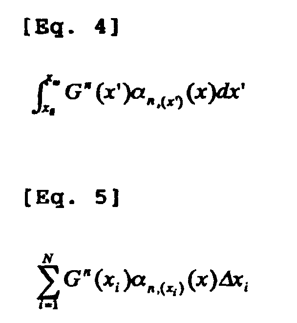
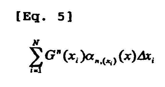
- equation 2 As an example of a method of particularly conducting calculations of the above described equation 1, equation 2 and equation 3 on a computer, a method is considered, in which an integral expressed by means of a described below equation 4 is made to be discrete as shown in a described below equation 5.
Landscapes
- Engineering & Computer Science (AREA)
- Physics & Mathematics (AREA)
- Theoretical Computer Science (AREA)
- Computer Hardware Design (AREA)
- Evolutionary Computation (AREA)
- Geometry (AREA)
- General Engineering & Computer Science (AREA)
- General Physics & Mathematics (AREA)
- Management, Administration, Business Operations System, And Electronic Commerce (AREA)
- Light Receiving Elements (AREA)
- Local Oxidation Of Silicon (AREA)
Abstract


Description


Claims (9)
- A simulation method of a breakdown, characterized in that the method comprises steps of:calculating an electric field distribution by means of a drift diffusion model;taking out a one-dimensional electric field distribution from a result of the calculation;providing the electric field distribution which was taken out to a one-dimensional Monte Carlo device simulation, calculating a distribution of impact ionization coefficients, and calculating Gn(x) using an equation 1 to an equation 5 described below

 determining that a breakdown does not occur in case that, as a result of this calculation, as n becomes to be large, Gn(x) converges to a constant value, and calculating a final electric current density; anddetermining that a breakdown occurs in case that Gn(x) becomes large as n increases.
 - A simulation method of a breakdown according to claim 1, characterized in that said electric field distribution is calculated by conducting a simulation by means of said drift diffusion model, in which an inverse bias is applied to a semiconductor element including an element isolating region.
- A simulation method of a breakdown according to claim 2, characterized in that said semiconductor element has a device structure including a two-dimensional diode structure.
- A simulation method of a breakdown according to claim 2, characterized in that said semiconductor element has a device structure including a three-dimensional diode structure.
- A simulation method of a breakdown according to claim 2, characterized in that said element isolating region is formed of a LOCOS.
- A simulation method of a breakdown according to claim 1, characterized in that said one-dimensional electric field distribution is taken out by cutting out a part in an electric field direction in one dimension, which has the largest electric field out of the calculated electric field distribution.
- A simulation method of a breakdown according to claim 6, characterized in that said part which has the largest electric field is an end portion of the element isolating region formed of said LOCOS.
- A simulation method of a breakdown, characterized in that the method comprises steps of:calculating an electric field distribution by means of a drift diffusion model;taking out a one-dimensional electric field distribution from a result of the calculation;providing the electric field distribution which was taken out to a one-dimensional Monte Carlo device simulation, calculating a distribution of impact ionization coefficients, and calculating Gn(x) using an equation 1 to an equation 5 described below
 determining that a breakdown does not occur in case that, as a result of thin calculation, as n becomes to be large. Gn(x) converges to a constant value, and calculating a final electric current density; anddetermining that a breakdown occurs in case that Gn(x) becomes to be large as n increases,
wherein said electric field distribution is calculated by conducting a simulation by means of said drift diffusion model, in which an inverse bias is applied to a semiconductor element including an element isolating region;said semiconductor element has a device structure including a two-dimensional diode structure;said element isolating region is formed of a LOCOS andsaid one-dimensional electric field distribution is taken out by cutting out a part in an electric field direction in one dimension, which has the largest electric field out of the calculated electric field distribution. - A simulation method of a breakdown, characterized in that the method comprises steps of:calculating an electric field distribution by means of a drift diffusion model;taking out a one-dimensional electric field distribution from a result of the calculation;providing the electric field distribution which was taken out to a one-dimensional Monte Carlo device simulation, calculating a distribution of impact ionization coefficients, and calculating Gn(x) using an equation 1 to an equation 5 described below

 determining that a breakdown does not occur in case that, as a result of this calculation, as ii becomes to be large, Gn(x) converges to a constant value, and calculating final electric current density; anddetermining that a breakdown occurs in case that Gn(x) becomes to be large as n increases,
wherein said electric field distribution is calculated by conducting a simulation by means of said drift diffusion model, in which an inverse bias is applied to a semiconductor element including an element isolating region;said semiconductor element has a device structure including a three-dimensional diode structure;said element isolating region is formed of a LOCOS;said one-dimensional electric field distribution is taken out by cutting out a part in an electric field direction in one dimension, which has the largest electric field out of the calculated electric field distribution andsaid part which has the largest electric field is an end portion of the element isolating region formed of said LOCOS.
Applications Claiming Priority (2)
| Application Number | Priority Date | Filing Date | Title |
|---|---|---|---|
| JP14465999 | 1999-05-25 | ||
| JP11144659A JP2000332264A (en) | 1999-05-25 | 1999-05-25 | Method for simulating breakdown |
Publications (2)
| Publication Number | Publication Date |
|---|---|
| EP1056025A2 true EP1056025A2 (en) | 2000-11-29 |
| EP1056025A3 EP1056025A3 (en) | 2007-11-28 |
Family
ID=15367244
Family Applications (1)
| Application Number | Title | Priority Date | Filing Date |
|---|---|---|---|
| EP00110841A Withdrawn EP1056025A3 (en) | 1999-05-25 | 2000-05-22 | Simultation method of breakdown in impact ionization |
Country Status (3)
| Country | Link |
|---|---|
| US (1) | US6681201B1 (en) |
| EP (1) | EP1056025A3 (en) |
| JP (1) | JP2000332264A (en) |
Cited By (1)
| Publication number | Priority date | Publication date | Assignee | Title |
|---|---|---|---|---|
| CN114068012A (en) * | 2021-11-15 | 2022-02-18 | 北京智精灵科技有限公司 | Cognitive decision-oriented multi-dimensional hierarchical drift diffusion model modeling method |
Families Citing this family (1)
| Publication number | Priority date | Publication date | Assignee | Title |
|---|---|---|---|---|
| RU2279152C1 (en) * | 2004-12-21 | 2006-06-27 | Государственное образовательное учреждение высшего профессионального образования "Орловский государственный технический университет" (ОрелГТУ) | Method for evaluating fact of cathodic breakdown initiation mechanism occurrence in case of vacuum breakdown |
Family Cites Families (5)
| Publication number | Priority date | Publication date | Assignee | Title |
|---|---|---|---|---|
| JPH08139151A (en) * | 1994-11-10 | 1996-05-31 | Mitsubishi Electric Corp | Method and apparatus for device simulation |
| JP2858559B2 (en) * | 1996-04-25 | 1999-02-17 | 日本電気株式会社 | Device simulation method |
| JP3003588B2 (en) * | 1996-09-18 | 2000-01-31 | 日本電気株式会社 | Ion implantation simulation method |
| JP3102556B2 (en) * | 1997-03-27 | 2000-10-23 | 日本電気株式会社 | Ion implantation simulation method |
| JP3221354B2 (en) * | 1997-04-11 | 2001-10-22 | 日本電気株式会社 | Device simulation method |
-
1999
- 1999-05-25 JP JP11144659A patent/JP2000332264A/en active Pending
-
2000
- 2000-05-22 EP EP00110841A patent/EP1056025A3/en not_active Withdrawn
- 2000-05-22 US US09/575,280 patent/US6681201B1/en not_active Expired - Lifetime
Cited By (2)
| Publication number | Priority date | Publication date | Assignee | Title |
|---|---|---|---|---|
| CN114068012A (en) * | 2021-11-15 | 2022-02-18 | 北京智精灵科技有限公司 | Cognitive decision-oriented multi-dimensional hierarchical drift diffusion model modeling method |
| CN114068012B (en) * | 2021-11-15 | 2022-05-10 | 北京智精灵科技有限公司 | Cognitive decision-oriented multi-dimensional hierarchical drift diffusion model modeling method |
Also Published As
| Publication number | Publication date |
|---|---|
| EP1056025A3 (en) | 2007-11-28 |
| JP2000332264A (en) | 2000-11-30 |
| US6681201B1 (en) | 2004-01-20 |
Similar Documents
| Publication | Publication Date | Title |
|---|---|---|
| Ferlet-Cavrois et al. | Statistical analysis of the charge collected in SOI and bulk devices under heavy lon and proton irradiation—Implications for digital SETs | |
| Nagai et al. | Structure and dynamics of magnetic reconnection for substorm onsets with Geotail observations | |
| Henry | ICP etching of silicon for micro and nanoscale devices | |
| Kunz et al. | Reduction of parasitic capacitance in vertical MOSFETs by spacer local oxidation | |
| Sutton et al. | An evaluation of transistor-layout RHBD techniques for SEE mitigation in SiGe HBTs | |
| US5652151A (en) | Method for determining an impurity concentration profile | |
| Zhou et al. | Understanding and optimizing EBIC pn-junction characterization from modeling insights | |
| Sai-Halasz et al. | Monte Carlo modeling of the transport of ionizing radiation created carriers in integrated circuits | |
| US6681201B1 (en) | Simulation method of breakdown | |
| US6034399A (en) | Electrostatic discharge protection for silicon-on-insulator | |
| Yamaguchi | Theoretical study of deep-trap-assisted anomalous currents in worst-bit cells of dynamic random-access memories (DRAM's) | |
| CN111460655B (en) | Analysis method and device for the influence of heavy ion radiation on the electrical parameters of SiC MOSFET | |
| Chia et al. | Impact ionization in Al x Ga 1− x As/GaAs single heterostructures | |
| Agarwal et al. | Impact ionization in thin silicon diodes | |
| Sengupta et al. | Effects of Incident Angle on Single-Event Leakage Current Degradation in Heavy-Ion Irradiated 1800 V and 4500 V SiC Power MOSFETs | |
| Burenkov et al. | A computationally efficient method for three-dimensional simulation of ion implantation | |
| CN103187411B (en) | The protective circuit of semiconductor device | |
| Kuehne et al. | SOI MOSFET with buried body strap by wafer bonding | |
| Matsuzawa et al. | Monte Carlo simulation of 50 nm devices with Schottky contact model | |
| Dai et al. | Leakage suppression of low-voltage transient voltage suppressor | |
| Ghin et al. | Monte Carlo Modelling of Impact Ionisation in GaAs | |
| Schröter et al. | Device Simulation | |
| JPH11204383A (en) | Simulation apparatus, simulation method, and computer-readable recording medium storing simulation program | |
| Brozek et al. | Charge injection using gate-induced-drain-leakage current for characterization of plasma edge damage in CMOS devices | |
| CN112903800B (en) | Semiconductor structure analysis method |
Legal Events
| Date | Code | Title | Description |
|---|---|---|---|
| PUAI | Public reference made under article 153(3) epc to a published international application that has entered the european phase |
Free format text: ORIGINAL CODE: 0009012 |
|
| AK | Designated contracting states |
Kind code of ref document: A2 Designated state(s): AT BE CH CY DE DK ES FI FR GB GR IE IT LI LU MC NL PT SE |
|
| AX | Request for extension of the european patent |
Free format text: AL;LT;LV;MK;RO;SI |
|
| RAP1 | Party data changed (applicant data changed or rights of an application transferred) |
Owner name: NEC ELECTRONICS CORPORATION |
|
| PUAL | Search report despatched |
Free format text: ORIGINAL CODE: 0009013 |
|
| AK | Designated contracting states |
Kind code of ref document: A3 Designated state(s): AT BE CH CY DE DK ES FI FR GB GR IE IT LI LU MC NL PT SE |
|
| AX | Request for extension of the european patent |
Extension state: AL LT LV MK RO SI |
|
| 17P | Request for examination filed |
Effective date: 20071218 |
|
| AKX | Designation fees paid |
Designated state(s): DE FR GB |
|
| 17Q | First examination report despatched |
Effective date: 20100331 |
|
| RAP1 | Party data changed (applicant data changed or rights of an application transferred) |
Owner name: RENESAS ELECTRONICS CORPORATION |
|
| STAA | Information on the status of an ep patent application or granted ep patent |
Free format text: STATUS: THE APPLICATION IS DEEMED TO BE WITHDRAWN |
|
| 18D | Application deemed to be withdrawn |
Effective date: 20100811 |