EP1055949A1 - Spiegel mit deformierbarer Membran - Google Patents
Spiegel mit deformierbarer Membran Download PDFInfo
- Publication number
- EP1055949A1 EP1055949A1 EP00401459A EP00401459A EP1055949A1 EP 1055949 A1 EP1055949 A1 EP 1055949A1 EP 00401459 A EP00401459 A EP 00401459A EP 00401459 A EP00401459 A EP 00401459A EP 1055949 A1 EP1055949 A1 EP 1055949A1
- Authority
- EP
- European Patent Office
- Prior art keywords
- membrane
- electrode
- substrate
- mirror
- layer
- Prior art date
- Legal status (The legal status is an assumption and is not a legal conclusion. Google has not performed a legal analysis and makes no representation as to the accuracy of the status listed.)
- Granted
Links
Images


Classifications
-
- G—PHYSICS
- G02—OPTICS
- G02B—OPTICAL ELEMENTS, SYSTEMS OR APPARATUS
- G02B26/00—Optical devices or arrangements for the control of light using movable or deformable optical elements
- G02B26/08—Optical devices or arrangements for the control of light using movable or deformable optical elements for controlling the direction of light
- G02B26/0816—Optical devices or arrangements for the control of light using movable or deformable optical elements for controlling the direction of light by means of one or more reflecting elements
- G02B26/0825—Optical devices or arrangements for the control of light using movable or deformable optical elements for controlling the direction of light by means of one or more reflecting elements the reflecting element being a flexible sheet or membrane, e.g. for varying the focus
Definitions
- the present invention relates to mirrors with deformable membrane.
- mirrors by modifying the geometry of their reflective surface under the action of a command exterior, transform some characteristics of the reflected beam to achieve, for example, a change of direction, a change spatial surface of the wave surface, phase shift, etc.
- Deformable membrane mirrors find applications in many fields (astronomy, optronic sights, ophthalmology, interferometry and holography, imagery in turbid environments, etc.) where they can be used to perform various functions and in particular for carrying out optical alignments (micro-positioning, harmonization of optical axes ...), micro-scans, beam stabilizations, micro focusing / defocusing, corrections of wave fronts (optical aberrations, turbulence, anamorphosis of beams %), phase shifts, etc ...
- the mirror shown in this figure 1 has a metallized membrane 1 carried by a substrate 2 which has a recess 2a.
- the membrane 1 closes said recess 2a and the bottom of said recess 2a carries, at membrane 1 right, a network of electrodes of command 2b.
- the metallized side of the membrane 1 - which is the face of said membrane which is not opposite the recess 2a - is maintained at a neutral potential, while control potentials Vi, Vj are applied to the different electrodes 2b, to generate on the membrane of the electrostatic forces which deforms it.
- Metallized membranes are usually in silicon nitride and the mirror components to deformable membrane are generally made by techniques conventionally known and used for the manufacture of integrated circuits based on Si3 N4 and in particular by depositing thin layers, photolithography, ionic or chemical machining, etc ...
- the invention aims to overcome these disadvantages.
- a mirror with deformable membrane of the type comprising a membrane which is carried by a substrate and of which at least one face is metallized, this substrate having two recesses closed on each other on either side of the metallized membrane, said mirror also comprising at at least two electrodes for controlling the deformation of the membrane, these two electrodes being arranged on either side of the membrane on the portions which define the funds of the recesses, that of these portions which is directly opposite the face metallized membrane being transparent.
- the invention provides a method for producing a mirror of this type
- the invention also provides a method for the realization of a mirror of the aforementioned type from a silicon wafer with integrated oxidized layer.
- silicon and technologies relating to silicon with integrated oxide allow make membranes of any shape (circular, square, hexagonal or more complex), with a very good accuracy, while allowing diameters of important mirror.
- a portion of substrate is produced by etching a silicon wafer with buried oxide layer (SOI).
- SOI buried oxide layer
- the invention also provides a mirror of the type cited above.
- a control electrode carried by said portion is a transparent electrode.
- Such a structure has the advantage of allowing distort any sign and double the amplitude of deformation at control voltage constant, while presenting a very good quality of reflection.
- the membrane is a silicon membrane and more particularly a silicon membrane with a thickness of around 3 ⁇ m or lower.
- Such a silicon membrane has low mechanical tensions which reduces the control voltages, for example at values from 100 to 150 V instead of voltages from 250 to 300 V for mirrors based on silicon nitride.
- a bottom portion on the side opposite the metallized face of the membrane carries a monolithic stack which includes a transparent electrode and a layer of photoconductive, said stack being able to be optically controlled to generate on the membrane a electrostatic field of complex profile while the electrodes on either side of the membrane are powered by a single power source.
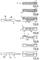
- FIG. 2 shows a component conforms to a possible embodiment of the invention.
- This component has a membrane 1 which extends between the recesses 2a, 3a of two glass slides 2 and 3 which are closed on top of each other.
- the blade 2 carries a single electrode 2b which extends at the bottom of its recess 2a, in line with the membrane 1.
- the blade 3 carries, in the bottom of its recess 3a, in line with the membrane 1, an array of electrodes 3b. On its face opposite the electrode 2b, the membrane 1 carries a metallization 5.
- This membrane 1 is 3 ⁇ m thick and is carried out in the manner which will now be described with reference to Figures 3a to 3g.
- This section 6 presents for example the following dimensional characteristics: diameter of on the order of 25 mm or more; total thickness of the order of 520 ⁇ m; buried oxidized layer (referenced by 7 on the figures) with a thickness of 0.5 ⁇ m and is located at a 20 ⁇ m deep.
- a first step we dop (p +) the face of the section 6 located on the side of the buried layer 7, the doped layer 8 thus produced being intended to define the membrane 1 3 ⁇ m thick, in the rest of the process.
- This same face is then metallized, for example by evaporation of a layer of aluminum or silver, so to get the mirror function.
- the recess 2a is produced by chemical etching. It is typically of a height of the order of 50 ⁇ m. The etching of this recess is preferably carried out with an accuracy of less than ⁇ m.
- blade 2 (as well as blade 3) is advantageously a silicon blade with layer buried oxide, which allows high precision of engraving.
- the electrode 2b deposited at the bottom of this recess 2a is optically transparent and is, for example, in indium tin oxide (ITO). She is for example vacuum deposited by evaporation or spraying cathodic.
- ITO indium tin oxide
- this counter electrode 2a is not subdivided and consists of a uniformly deposited layer over substantially the entire bottom of the recess 2a.
- the buried oxidized layer 7 having for function of selectively stopping this engraving.
- the barrier layer that this layer constitutes buried thus allows the etching of silicon with great precision that it would not be possible to achieve for such a thickness with silicon pure.
- SOI silicon oxide wafers integrated
- the next step is (figure 3e) to open, by photolithography and chemical attack, a window in the oxidized layer 7, at the level of the recess 2a and at etch non-oxidized silicon by chemical attack as well discovered, over a thickness of 20 ⁇ m. This thickness is very well controlled because the chemical attack is blocked by the p + doping layer previously obtained.
- the component obtained after these first steps have many advantages.
- the unetched portions of the layer oxidized define a reference surface of a large precision, which, as we will see later in a more detailed, is used for the assembly of a second electrode.
- the membrane 1 is released by a final etching step which only works on a very small thickness, it is possible to consider for the membrane forms very varied, without being limited by the anisotropic effects of chemical attack in crystalline media.
- the membrane 1 thus obtained at the end of these first steps is not flat, but is drawn into the recess 2a due to the pressure difference between the two sides of this membrane 1.
- Atmospheric pressure is restored on the one hand and on the other side of the membrane 1, leaving an opening for small dimension (not shown) in the thickness of the glass slide 2 (Figure 3f). This opening is also used to introduce an electrical contact on the ITO layer serving as a counter electrode.
- blade 3 is done, substantially in the same way as for blade 2, by making a chemical etching, over a thickness which is typically of the order of 50 ⁇ m, then by depositing a network of electrodes 3b in the bottom of the recess 3a as well form.
- blade 3 does not need to be transparent and could be any other material than glass and especially any other material electrically insulating.
- a glass substrate offers the advantage a proven ion weld assembly.
- the electrode network 3b is produced by deposition under vacuum of a metallic layer (Aluminum by example). This layer is then masked, then etched chemically by lithography.
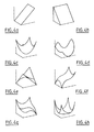
- the electrodes 3b do not have uniform dimensions and geometries but are optimized according to the basic deformations that the mirror must be able to withstand.
- an optimized electrode network is of the type that shown in FIG. 5: it includes a central electrode 9 of square shape, surrounded by twelve peripheral electrodes 10, also of square shape, whose side length is equal to half the length of side of the central electrode 9.
- the control voltages applied between the electrode 2b and the network of electrodes 3b are very substantially reduced compared to those required for components based on silicon nitride.
- Tensions of 100 V is sufficient to obtain distortions of a few micrometers, to be compared to voltages of 250 V for components based on silicon nitride.
- silicon membranes allow to consider deformations of greater amplitudes for more restrictive applications. It is indeed possible, by applying control voltages comparable to those used with membranes in silicon nitride (250 V) to obtain deformed shapes having higher amplitudes (> 10 ⁇ m).
- said electrode 2b is advantageously covered by an anti-reflection layer.
- this etching of a bellows is for example carried out before the doping and metallization deposition step on the slice of SELF.
- the bellows is for example constituted by one or more circular grooves 11 engraved on a silicon thickness of 20 ⁇ m.
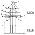
- the electrodes of the network 3b can be replaced by a single electrode optically controlled.
- the single electrode (from ITO for example) - referenced by 3c - is deposited in the bottom of the recess 3a of the blade 3, on a layer of material photo-conductor 12 to which it is thus coupled.
- a light source 13 for example a lamp incandescent, illuminates a mask 14 through a Streamer.
- This mask 14 is representative of the distribution and shape of the electrostatic field that we want to create on the silicon membrane.
- the picture of this mask is projected by a lens 15 onto the blade 3 in glass supporting the electrode 3c.
- the photoconductor can be a mineral layer (for example a silicon bismuth oxide Bi12 SiO20) or an organic layer (for example polyvinyl carbozole PVK).
- a mineral layer for example a silicon bismuth oxide Bi12 SiO20
- an organic layer for example polyvinyl carbozole PVK
- This conductivity then has a distribution of the type illustrated in FIG. 7b
- Thin thickness (1 ⁇ m to a few micrometers) of the photoconductive layer 12 makes it possible to preserve a excellent spatial resolution. Spatial distribution of the electrical voltage is reproduced faithfully at from the spatial distribution of intensity bright incident.
- controllable electrode optically requires an optical addressing system additional, which may not be accepted for some applications this approach can be optionally used for applications requiring generation of complex deformities that cannot be obtained with a simple network of electrodes.
- This concept also allows the generation of a profile continuous field of electrostatic forces. For it, just choose a mask whose transparency is not not binary but at N gray levels. Ultimately, the transparency of the mask can be analog with a continuous variation of its opacity. On the other hand, the mask can have a dynamic function of the transparency. Instead of using a mask where the spatial transparency is frozen once and for all, we may, for certain applications, use a mask dynamic whose transfer function evolves temporally.
- This specificity can be taken advantage of for applications requiring the generation of deformed shapes dynamics reproducing a sequence whose functions transfer, spatial and temporal, are recorded beforehand.
- Another variant of the electrical control can be considered in case it is necessary to increase the number of electrodes of the network 3b. If this number of electrodes is high, for example of the order of 100 or higher, in addition to the complexity of the order electric, there is the problem of access to different studs. This problem is well known in particular by liquid crystal display designers for the visualization. Matrix access to address each coordinate point X, Y can use lines and columns, each powered by voltages: + V / 2, -V / 2 or 0. But this principle, besides the fact that requires a threshold effect that does not exist in application to deformation membranes electrostatic, is not compatible with large number of electrodes. Indeed, in the absence of an effect memory, control voltage cannot be applied only on one line at a time. In the case of visualization, a device consists in multiplexing electric control. this is not too annoying for the observer, who integrates temporally the images of each line thanks to the retinal remanence.
- One approach is to create local memory attached to each point (pixel for viewing, zonal electrode for MMA).
- command matrices like those used in the field of flat screens and in particular control matrices using TFT technology (Thin Film Transistor).
Applications Claiming Priority (2)
| Application Number | Priority Date | Filing Date | Title |
|---|---|---|---|
| FR9906709 | 1999-05-27 | ||
| FR9906709A FR2794251B1 (fr) | 1999-05-27 | 1999-05-27 | Miroir a membrane deformable |
Publications (2)
| Publication Number | Publication Date |
|---|---|
| EP1055949A1 true EP1055949A1 (de) | 2000-11-29 |
| EP1055949B1 EP1055949B1 (de) | 2005-11-09 |
Family
ID=9546068
Family Applications (1)
| Application Number | Title | Priority Date | Filing Date |
|---|---|---|---|
| EP20000401459 Expired - Lifetime EP1055949B1 (de) | 1999-05-27 | 2000-05-25 | Spiegel mit deformierbarer Membran |
Country Status (3)
| Country | Link |
|---|---|
| EP (1) | EP1055949B1 (de) |
| DE (1) | DE60023788T2 (de) |
| FR (1) | FR2794251B1 (de) |
Cited By (3)
| Publication number | Priority date | Publication date | Assignee | Title |
|---|---|---|---|---|
| WO2002091060A2 (fr) * | 2001-05-10 | 2002-11-14 | Jean-Pierre Lazzari | Dispositif de modulation de lumiere |
| WO2004038877A2 (en) * | 2002-10-07 | 2004-05-06 | Coherent, Inc. | Tunable optically-pumped semiconductor laser including a polarizing resonator mirror |
| WO2011051755A1 (en) * | 2009-10-30 | 2011-05-05 | Consiglio Nazionale Delle Ricerche | Optically controlled deformable reflective/refractive assembly with photoconductive substrate |
Citations (4)
| Publication number | Priority date | Publication date | Assignee | Title |
|---|---|---|---|---|
| EP0046873A1 (de) * | 1980-09-02 | 1982-03-10 | Texas Instruments Incorporated | Lichtmodulator mit verformbarem Spiegel |
| US5022745A (en) * | 1989-09-07 | 1991-06-11 | Massachusetts Institute Of Technology | Electrostatically deformable single crystal dielectrically coated mirror |
| US5774252A (en) * | 1994-01-07 | 1998-06-30 | Texas Instruments Incorporated | Membrane device with recessed electrodes and method of making |
| US5822110A (en) * | 1994-09-02 | 1998-10-13 | Dabbaj Rad H | Reflective light valve modulator |
-
1999
- 1999-05-27 FR FR9906709A patent/FR2794251B1/fr not_active Expired - Fee Related
-
2000
- 2000-05-25 EP EP20000401459 patent/EP1055949B1/de not_active Expired - Lifetime
- 2000-05-25 DE DE2000623788 patent/DE60023788T2/de not_active Expired - Fee Related
Patent Citations (5)
| Publication number | Priority date | Publication date | Assignee | Title |
|---|---|---|---|---|
| EP0046873A1 (de) * | 1980-09-02 | 1982-03-10 | Texas Instruments Incorporated | Lichtmodulator mit verformbarem Spiegel |
| US5022745A (en) * | 1989-09-07 | 1991-06-11 | Massachusetts Institute Of Technology | Electrostatically deformable single crystal dielectrically coated mirror |
| US5774252A (en) * | 1994-01-07 | 1998-06-30 | Texas Instruments Incorporated | Membrane device with recessed electrodes and method of making |
| US5822110A (en) * | 1994-09-02 | 1998-10-13 | Dabbaj Rad H | Reflective light valve modulator |
| US5822110C1 (en) * | 1994-09-02 | 2001-06-26 | Dabbaj Rad Hassan | Reflective light valve modulator |
Cited By (6)
| Publication number | Priority date | Publication date | Assignee | Title |
|---|---|---|---|---|
| WO2002091060A2 (fr) * | 2001-05-10 | 2002-11-14 | Jean-Pierre Lazzari | Dispositif de modulation de lumiere |
| FR2824643A1 (fr) * | 2001-05-10 | 2002-11-15 | Jean Pierre Lazzari | Dispositif de modulation de lumiere |
| WO2002091060A3 (fr) * | 2001-05-10 | 2003-04-03 | Jean-Pierre Lazzari | Dispositif de modulation de lumiere |
| WO2004038877A2 (en) * | 2002-10-07 | 2004-05-06 | Coherent, Inc. | Tunable optically-pumped semiconductor laser including a polarizing resonator mirror |
| WO2004038877A3 (en) * | 2002-10-07 | 2004-07-08 | Coherent Inc | Tunable optically-pumped semiconductor laser including a polarizing resonator mirror |
| WO2011051755A1 (en) * | 2009-10-30 | 2011-05-05 | Consiglio Nazionale Delle Ricerche | Optically controlled deformable reflective/refractive assembly with photoconductive substrate |
Also Published As
| Publication number | Publication date |
|---|---|
| EP1055949B1 (de) | 2005-11-09 |
| DE60023788T2 (de) | 2006-06-08 |
| FR2794251B1 (fr) | 2002-08-02 |
| FR2794251A1 (fr) | 2000-12-01 |
| DE60023788D1 (de) | 2005-12-15 |
Similar Documents
| Publication | Publication Date | Title |
|---|---|---|
| EP0610185B1 (de) | Vorrichtung zur optischen modulation mit verformbaren zellen | |
| EP2548054B1 (de) | Brechungskombinierer für eine headup-farbanzeigevorrichtung | |
| FR2820834A1 (fr) | Procede de fabrication d'un micro-miroir optique et micro-miroir ou matrice de micro-miroirs obtenu par ce procede | |
| EP3239671B1 (de) | Vorrichtung zur erfassung von elektromagnetischer strahlung mit einer einkapselungsstruktur, die mindestens einen interferenzfilter umfasst | |
| FR2989518A1 (fr) | Procede de fabrication d'un capteur d'image a surface courbe | |
| WO2015091836A1 (fr) | Dispositif optique pour la stabilisation d'images | |
| EP2591324A1 (de) | Wellenfrontanalysator mit flüssigkristall-mikrolinsen | |
| EP1055949B1 (de) | Spiegel mit deformierbarer Membran | |
| CA2584239C (fr) | Miroir deformable | |
| FR2820833A1 (fr) | Micro-miroir optique a pivot, matrice de tels micro-miroirs et procede de realisation dudit micro-miroir | |
| EP0742459A1 (de) | Optomechanischer Mikro-Strahlablenker unter Verwendung der Verschiebung von Mikrolinsen | |
| EP1008892A1 (de) | Halbleiterphasenmodulator | |
| EP3123212B1 (de) | Optische vorrichtung mit einer deformierbaren membran | |
| WO2021170708A1 (fr) | Ecran d'affichage à résolution multiple et procédé de réalisation | |
| EP1697783A1 (de) | Optische komponenten und herstellung dafür | |
| WO2021228744A1 (fr) | Ecran pour l'affichage d'une image projetee comportant un revetement structure | |
| EP1275020A1 (de) | Optischer schalter mit bewegbaren teilen und verfahren zu seiner herstellung | |
| EP3764148A1 (de) | Scanner mit optischer netzeinheit mit mobiler phasensteuerung | |
| WO2021165608A1 (fr) | Composant optique à métasurface encapsulée et procédé de fabrication d'un tel composant | |
| EP4070139A1 (de) | Adaptives optisches system mit verbesserter antwortzeit, zugehörige verwendung und verfahren | |
| FR2702851A1 (fr) | Modulateur de lumière à cristal liquide ferroélectrique et à adressage optique. | |
| EP1042813A1 (de) | Halbleiterschaltung mit einem originalen, isolierenden und transparenten substrat | |
| FR2835062A1 (fr) | Commutateur optique a micro-miroir et son procede de realisation | |
| EP1097398A1 (de) | Anzeigevorrichtung mit sehr kleinem verbrauch | |
| FR2742224A1 (fr) | Capteur a base de silicium et procede de fabrication |
Legal Events
| Date | Code | Title | Description |
|---|---|---|---|
| PUAI | Public reference made under article 153(3) epc to a published international application that has entered the european phase |
Free format text: ORIGINAL CODE: 0009012 |
|
| AK | Designated contracting states |
Kind code of ref document: A1 Designated state(s): DE FR GB IT |
|
| AX | Request for extension of the european patent |
Free format text: AL;LT;LV;MK;RO;SI |
|
| 17P | Request for examination filed |
Effective date: 20010514 |
|
| AKX | Designation fees paid |
Free format text: DE FR GB IT |
|
| 17Q | First examination report despatched |
Effective date: 20040422 |
|
| GRAP | Despatch of communication of intention to grant a patent |
Free format text: ORIGINAL CODE: EPIDOSNIGR1 |
|
| GRAS | Grant fee paid |
Free format text: ORIGINAL CODE: EPIDOSNIGR3 |
|
| GRAA | (expected) grant |
Free format text: ORIGINAL CODE: 0009210 |
|
| RAP1 | Party data changed (applicant data changed or rights of an application transferred) |
Owner name: SAGEM SA |
|
| AK | Designated contracting states |
Kind code of ref document: B1 Designated state(s): DE FR GB IT |
|
| REG | Reference to a national code |
Ref country code: GB Ref legal event code: FG4D Free format text: NOT ENGLISH |
|
| REF | Corresponds to: |
Ref document number: 60023788 Country of ref document: DE Date of ref document: 20051215 Kind code of ref document: P |
|
| GBT | Gb: translation of ep patent filed (gb section 77(6)(a)/1977) |
Effective date: 20060227 |
|
| RAP2 | Party data changed (patent owner data changed or rights of a patent transferred) |
Owner name: SAGEM DEFENSE SECURITE |
|
| PLBE | No opposition filed within time limit |
Free format text: ORIGINAL CODE: 0009261 |
|
| STAA | Information on the status of an ep patent application or granted ep patent |
Free format text: STATUS: NO OPPOSITION FILED WITHIN TIME LIMIT |
|
| 26N | No opposition filed |
Effective date: 20060810 |
|
| REG | Reference to a national code |
Ref country code: GB Ref legal event code: 732E |
|
| PGFP | Annual fee paid to national office [announced via postgrant information from national office to epo] |
Ref country code: IT Payment date: 20090424 Year of fee payment: 10 Ref country code: DE Payment date: 20090603 Year of fee payment: 10 |
|
| PGFP | Annual fee paid to national office [announced via postgrant information from national office to epo] |
Ref country code: GB Payment date: 20090427 Year of fee payment: 10 |
|
| GBPC | Gb: european patent ceased through non-payment of renewal fee |
Effective date: 20100525 |
|
| PG25 | Lapsed in a contracting state [announced via postgrant information from national office to epo] |
Ref country code: IT Free format text: LAPSE BECAUSE OF NON-PAYMENT OF DUE FEES Effective date: 20100525 |
|
| PG25 | Lapsed in a contracting state [announced via postgrant information from national office to epo] |
Ref country code: DE Free format text: LAPSE BECAUSE OF NON-PAYMENT OF DUE FEES Effective date: 20101201 |
|
| PG25 | Lapsed in a contracting state [announced via postgrant information from national office to epo] |
Ref country code: GB Free format text: LAPSE BECAUSE OF NON-PAYMENT OF DUE FEES Effective date: 20100525 |
|
| PGFP | Annual fee paid to national office [announced via postgrant information from national office to epo] |
Ref country code: FR Payment date: 20120625 Year of fee payment: 13 |
|
| REG | Reference to a national code |
Ref country code: FR Ref legal event code: ST Effective date: 20140131 |
|
| PG25 | Lapsed in a contracting state [announced via postgrant information from national office to epo] |
Ref country code: FR Free format text: LAPSE BECAUSE OF NON-PAYMENT OF DUE FEES Effective date: 20130531 |