CROSS REFERENCE TO RELATED APPLICATIONS
-
This application is a continuation in part of patent application serial
number 09/191,865 (Attorney Docket number VGO-115) , filed by Knittel et al.
on Nov. 12, 998, and entitled "TWO-LEVEL MINI-BLOCK STORAGE
SYSTEM FOR VOLUME DATA SETS."
FIELD OF INVENTION
-
The invention relates generally to the field of computer graphics, and
particularly to a voxel memory controlled by a state machine.
FIELD OF INVENTION
-
The present invention is related to the field of computer graphics, and in
particular to a volume graphics memory interfaced to multiple volume rendering
pipelines.
BACKGROUND OF THE INVENTION
-
Volume graphics is the subfield of computer graphics that deals with the
visualization of objects or phenomena represented as sampled data in three or
more dimensions. These samples are called volume elements, or "voxels," and
contain digital information representing physical characteristics of the objects
or phenomena being studied. For example, voxel values for a particular object
or system may represent density, type of material, temperature, velocity, or
some other property at discrete points in space throughout the interior and in the
vicinity of that object or system.
-
Volume rendering is the part of volume graphics concerned with the
projection of volume data as two-dimensional images for purposes of printing,
display on computer terminals, and other forms of visualization. By assigning
colors and transparency to voxel data values, different view directions of the
exterior and interior of an object or system can be displayed. For example, a
surgeon needing to examine the ligaments, tendons, and bones of a human knee in
preparation for surgery can utilize a tomographic scan of the knee and cause voxel
data values corresponding to blood, skin, and muscle to appear to be completely
transparent.
-
The resulting image then reveals the condition of the ligaments, tendons,
bones, etc. which are hidden from view prior to surgery, thereby allowing for
better surgical planning, shorter surgical operations, less surgical exploration and
faster recoveries. In another example, a mechanic using a tomographic scan of a
turbine blade or welded joint in a jet engine can cause voxel data values
representing solid metal to appear to be transparent while causing those
representing air to be opaque. This allows the viewing of internal flaws in the
metal that would otherwise be hidden from the human eye.
-
Real-time volume rendering is the projection and display of volume data as
a series of images in rapid succession, typically at 24 or 30 frames per second or
faster. This makes it possible to create the appearance of moving pictures of the
object, phenomenon, or system of interest. It also enables a human operator to
interactively control the parameters of the projection and to manipulate the image,
thus providing the user with immediate visual feedback. It will be appreciated that
projecting tens of millions or hundreds of millions of voxel values to an image
requires enormous amounts of computing power. Doing so in real-time requires
substantially more computational power.
-
Additional general background on volume rendering is presented in a book
entitled "Introduction to Volume Rendering" by Barthold Lichtenbelt, Randy
Crane, and Shaz Naqvi, published in 1998 by Prentice Hall PTR of Upper Saddle
River, New Jersey. Further background on volume rendering architectures is
found in a paper entitled "Towards a Scalable Architecture for Real-time Volume
Rendering" presented by H. Pfister, A. Kaufman, and T. Wessels at the 10th
Eurographics Workshop on Graphics Hardware at Maastricht, The Netherlands,
on August 28 and 29, 1995. This paper describes an architecture now known as
"Cube 4."
-
The Cube 4 is also described in a Doctoral Dissertation entitled
"Architectures for Real-Time Volume Rendering" submitted by Hanspeter Pfister
to the Department of Computer Science at the State University of New York at
Stony Brook in December 1996, and in U.S. Patent No. 5,594,842, "Apparatus
and Method for Real-time Volume Visualization."
-
The task of designing a flexible and efficient interface between a memory
where the volume data set is stored, and a processor which renders the volume
as a real-time sequence of images needs to address two problems. First, the
arrangement of the voxels in the data set must maximize parallelism regardless
of view direction, where the processor permits it, taking into considerations
physical access limitations inherent in semiconductor memory devices.
Maximizing parallelism increases the bandwidth of the interface. Second, the
transfer of data from the memory to the processor must take maximum
advantage of the inherent bandwidth of the memory and minimize transfer
delays due to synchronization requirements in a pipelined processor. Delays
cause stalls.
SUMMARY OF THE INVENTION
-
A state machine controls accesses to a voxel memory in a graphics
rendering system. The accesses include pipeline accesses, host accesses and
maintenance accesses. According to one aspect of the invention, accesses by the
pipelines have priority over all other accesses of the voxel memory. With such
an arrangement, it is ensured that render operations are performed as quickly as
possible, thereby ensuring that real-time rendering rates are achievable.
-
The voxel memory stores a volume data set to be processed by rendering
pipelines. The state machine includes a refresh state to periodically maintain
data in the memory, a render state for synchronously transferring data from the
memory to a plurality of rendering pipelines, a read state for asynchronously
transferring data from the memory to a host computer; and a write state for
asynchronously transferring data from the host computer to the memory.
-
The state machine decodes memory access requests, the requests
including render, read, write, and maintenance requests. The render requests
have priority over the maintenance requests, which have priority over the read
and write requests.
BRIEF DESCRIPTION OF THE DRAWINGS
-
The foregoing features of this invention, as well as the invention itself, may
be more fully understood from the following Detailed Description of the
Invention, and Drawing, of which:
- Figure 1 is a diagrammatic illustration of a volume data set and respective
coordinate systems;
- Figure 2 is a diagrammatic illustration of a view of a volume data set being
projected onto an image plane by means of ray-casting;
- Figure 3 is a cross-sectional view of the volume data set of Figure 2;
- Figure 4 is a diagrammatic illustration of the processing of an individual
ray by ray-casting;
- Figure 5A is a block diagram of one embodiment of a pipelined processing
element for real-time volume rendering in accordance with the present invention;
- Figure 5B is a block diagram of a second embodiment of a portion of the
pipelined processing element of Figure 5A;
- Figure 6 is a block diagram of the logical layout of a volume graphics
system including a host computer coupled to a volume graphics board operating
in accordance with the present invention;
- Figure 7 is a block diagram of the general layout of a volume rendering
integrated circuit on the circuit board of Figure 6, where the circuit board
includes the processing pipelines of Figures 5A or 5B;
- Figure 8 illustrates how a volume data set is organized into sections;
- Figure 9 is a block diagram of the volume rendering integrated circuit of
Figure 7 showing parallel processing pipelines such as those of Figures 5A and
5B;
- Figure 10 is a timing diagram for illustrating the forwarding of voxels from
a memory interface to the integrated circuit of Figure 7;
- Figure 11 is a diagrammatic representation of the mapping of voxels
comprising a mini-block to an SDRAM;
- Figure 12 is a diagrammatic representation of mini-blocks in memory;
- Figure 13 is a diagrammatic representation of mini-blocks within the banks
and rows of the DRAMs;
- Figure 14 is provided to illustrate one method of rendering a sectioned data
set such as that described in Figure 8;
- Figure 15 is a block diagram of one embodiment of a voxel memory
interface provided in the integrated circuit of Figure 7;
- Figure 16 is a block diagram of one embodiment of a memory controller
provided in the voxel memory interface of Figure 15;
- Figure 17 is a state diagram illustrating the various interrelationships of
states in a state machine of the memory controller of Figure 16;
- Figure 18 is a block diagram of one embodiment of a traverser that is used
to provide an address to the memory controller of Figure 16;
- Figure 19 illustrates exemplary mappings of a transform register that is
used to generate and address at the traverser of Figure 18;
- Figure 20 is a block diagram of deskewing logic that is provided in the
memory interface of Figure 15;
- Figure 21 is a table illustrating exemplary skewed voxel orders that are
deskewed using the deskewing logic of Figure 20;
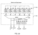
- Figure 22 illustrates a relationship between voxels stored as a mini-beam
and voxels retrieved as slices during the processing of a volume data set; and
- Figure 23A is a block diagram of one embodiment of slice buffer and
output logic used in the memory interface of Figure 15.
-
DETAILED DESCRIPTION OF PREFERRED EMBODIMENTS
-
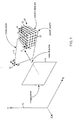
Referring now to Figure 1, a view of a three-dimensional volume data set
10 is shown. Figure 1 depicts an array of voxel positions 12 arranged in the form
of a rectangular solid 10. More particularly, the voxel positions fill the solid in
three dimensions and are uniformly spaced in a particular dimension. Associated
with each voxel position is one or more data values representing some
characteristics of an object, system, or phenomenon under study, for example
density, type of material, temperature, velocity, opacity or other properties at
discrete points in space throughout the interior and in the vicinity of that object or
system.
-
A brief description of the basic coordinate system used herein, and the
relationship between the coordinates and the planes will first be described. There
are four basic coordinate systems in which the voxels of the data set may be
referenced - object coordinates (u,v,w), permuted coordinates (x,y,z), base plane
coordinates (xb,yb,zb), and image space coordinates (xi, yi,zi). The object and image
space coordinates are typically right-handed coordinate systems. The permuted
coordinate system may be either right-handed or left-handed, depending upon a
selected view direction.
-
The volume data set is an array of voxels defined in object coordinates with
axes u, v, and w as indicated at 9. The origin is located at one corner of the
volume, typically a corner representing a significant starting point from the
object's own point of view. The voxel at the origin is stored at the base address of
the volume data set stored in a memory, as will be described later herein. Any
access to a voxel in the volume data set is expressed in terms of u, v and w, which
are then used to obtain an offset from this address. The unit distance along each
axis equals the spacing between adjacent voxels along that axis. In Figure 1 the
volume data set is represented as a cube 10.
-
Figure 1 illustrates an example of a volume data set 10. It is rotated so that
the origin of the object is in the upper, right, rear corner. That is, the object
represented by the data set is being viewed from the back, at an angle. In the
permuted coordinate system (x,y,z), represented by 11, the origin is repositioned
to the vertex of the volume nearest the image plane 5, where the image plane is a
two-dimensional viewing surface. The z-axis is the edge of the volume most
nearly parallel to the view direction. The x-and y-axes are selected such that the
traversal of voxels in the volume data set 10 always occurs in a positive direction.
In Figure 1, the origin of the permuted coordinate system is the opposite corner of
the volume from the object's own origin.
-
The base plane coordinate system coordinates (xb, yb, zb) is a system in
which the zb = 0 plane is co-planar with the xy-face of the volume data set in
permuted coordinates. The base plane 7 is a finite plane that extends from the base
plane origin to a maximum point that depends upon both the size of the volume
data set and upon the view direction.
-
The image space coordinate system (xi, yi,zi), represented at 15, is the
coordinate system of the final image resulting from rendering the volume. The
zi=0 plane 5 is the plane of the computer screen, printed page or other medium on
which the volume is to be displayed.
-
By way of example, Figure 2 illustrates the volume data set 10 as
comprising an array of slices from a tomographic scan of the human head. A two-dimensional
image plane 16 represents the surface on which a volume rendered
projection of the human head is to be displayed. In a technique known as ray-casting,
rays 18 are cast from pixel positions 22 on the image plane 16 through the
volume data set 10, with each ray accumulating color and opacity from the data at
voxel positions as it passes through the volume. In this manner, the color,
transparency, and intensity as well as other parameters of a pixel are extracted
from the volume data set as the accumulation of data at sample points 20 along
the ray. In this example, voxel values associated with bony tissue are assigned an
opaque color, and voxel values associated with all other tissue in the head are
assigned a transparent color. Therefore, the accumulation of data along a ray and
the attribution of this data to the corresponding pixel result in an image 19 in
viewing plane 16 that appears to an observer to be an image of a three-dimensional
skull, even though the actual skull is hidden from view by the skin
and other tissue of the head.
-
In order to appreciate more fully the method of ray-casting, Figure 3
depicts a two-dimensional cross-section of the three-dimensional volume data set
10. The first and second dimensions correspond to the dimensions illustrated on
the plane of the page. The third dimension of volume data set 10 is perpendicular
to the printed page so that only a cross section of the data set can be seen in the
figure. Voxel positions are illustrated by dots 12 in the figure. The voxels
associated with each position are data values that represent some characteristic or
characteristics of a three-dimensional object 14 at fixed points of a rectangular
grid in three-dimensional space. Also illustrated in Figure 3 is a one-dimensional
view of a two-dimensional image plane 16 onto which an image of object 14 is to
be projected in terms of pixels 22 with the appropriate characteristics. In this
illustration, the second dimension of image plane 16 is also perpendicular to the
printed page.
-
In the technique of ray-casting, rays 18 are extended from pixels 22 of the
image plane 16 through the volume data set 10. Each ray accumulates color,
brightness, and transparency or opacity at sample points 20 along that ray. This
accumulation of light determines the brightness and color of the corresponding
pixels 22. Thus, while the ray is depicted going outwardly from a pixel through
the volume, the accumulated data can be thought of as being transmitted back
down the ray where it is provided to the corresponding pixel to give the pixel
color, intensity and opacity or transparency, amongst other parameters. It will be
appreciated that although Figure 3 suggests that the third dimension of volume
data set 10 and the second dimension of image plane 16 are both perpendicular to
the printed page and therefore parallel to each other, in general this is not the case.
The image plane may have any orientation with respect to the volume data set, so
that rays 18 may pass through volume data set 10 at any angle in all three
dimensions.
-
It will also be appreciated that sample points 20 do not necessarily intersect
the voxel 12 coordinates exactly. Therefore, the value of each sample point must
be synthesized from the values of voxels nearby. That is, the intensity of light,
color, and transparency or opacity at each sample point 20 must be calculated or
interpolated as a mathematical function of the values of nearby voxels 12. The re-sampling
of voxel data values to values at sample points is an application of the
branch of mathematics known as sampling theory. The sample points 20 of each
ray 18 are then accumulated by another mathematical function to produce the
brightness and color of the pixel 22 corresponding to that ray. The resulting set of
pixels 22 forms a visual image of the object 14 in the image plane 16.
-
Figure 4 illustrates the processing of an individual ray. Ray 18 passes
through the three-dimensional volume data set 10 at some angle, passing near or
possible through voxel positions 12, and accumulates data at sample points 20
along each ray. The value at each sample point is synthesized as illustrated at 21
by an interpolation unit 103 (see Figure 5A), and its gradient is calculated as
illustrated at 23 by a gradient estimation unit 111 (see Figure 5A). The sample
point values from sample point 20 and the gradient 25 for each sample point are
then processed to assign color, brightness or intensity, and transparency or opacity
to each sample. As illustrated at 27, this is done via processing in which red, green
and blue hues as well as intensity and opacity or transparency are calculated.
Finally, the colors, levels of brightness, and transparencies assigned to all of the
samples along all of the rays are applied as illustrated at 29 to a compositing unit
124 (of Figure 5a) that mathematically combines the sample values into pixels
depicting the resulting image 32 for display on image plane 16.
-
The calculation of the color, brightness or intensity, and transparency of
sample points 20 is done in two parts. In one part, a mathematical function such as
trilinear interpolation is utilized to take the weighted average of the values of the
eight voxels in a cubic arrangement immediately surrounding the sample point 20.
The resulting average is then used to assign a color and opacity or transparency to
the sample point by some transfer function. In the other part, the mathematical
gradient of the sample values at each sample point 20 is estimated by a method
such as taking the differences between nearby sample points. It will be
appreciated that these two calculations can be implemented in either order or in
parallel with each other to produce mathematically equivalent results. The
gradient is then used in a lighting calculation to determine the brightness of the
sample point. Lighting calculations are well-known in the computer graphics art
and are described, for example, in the textbook "Computer Graphics: Principles
and Practice," 2nd edition, by J. Foley, A. vanDam, S. Feiner, and J. Hughes,
published by Addison-Wesley of Reading, Massachusetts, in 1990.
-
Figure 5A depicts a block diagram of one embodiment of a pipelined
processor appropriate for performing the calculations illustrated in Figure 4. The
pipelined processor includes a plurality of pipeline stages, each stage of which
holds one data element, so that a plurality of data elements are being processed at
one time. Each data element is at a different degree of progress in its processing,
and all data elements move from stage to stage of the pipeline in lock step. At the
first stage of the pipeline, a series of voxel data values flow into the pipeline at a
rate of one voxel per cycle from the voxel memory 100, which operates under the
control of an address generator 102. The voxels arrive from the memory via a
communications channel and memory interface described in greater detail below.
-
The interpolation unit 104 receives voxel values located at coordinates x-,
y- and z-in three-dimensional space, where x, y, and z are each integers. The
interpolation unit 104 is a set of pipelined stages that synthesize data values at
sample points between voxels corresponding to positions along rays that are cast
through the volume. During each cycle, one voxel enters the interpolation unit and
one interpolated sample value emerges. The latency between the time a voxel
value enters the pipeline and the time that an interpolated sample value emerges
depends upon the number of pipeline stages and the internal delay in each stage.
-
The interpolation stages of the pipeline comprise a set of interpolator stages
104 and three FIFO elements 106, 108, 110. The FIFOs delay data in the stages so
that the data can be combined with later arriving data. In the current embodiment,
these are all linear interpolations, but other interpolation functions such as cubic
and LaGrangian may also be employed. In the illustrated embodiment,
interpolation is performed in each dimension as a separate stage, and the
respective FIFO elements are included to delay data for purposes of interpolating
between voxels that are adjacent in space but widely separated in the time of entry
to the pipeline. The delay of each FIFO is selected to be exactly the amount of
time elapsed between the reading of one voxel and the reading of an adjacent
voxel in that particular dimension so that the two can be combined in an
interpolation function.
-
It will be appreciated that voxels can be streamed through the interpolation
stage at a rate of one voxel per cycle with each voxel being combined with the
nearest neighbor that had been previously delayed through the FIFO associated
with that dimension. It will also be appreciated that in a semiconductor
implementation, these and other FIFOs can be implemented as random access
memories.
-
Three successive interpolation stages, one for each dimension, are
concatenated and voxels can pass through the three stages at a rate of one voxel
per cycle at both the input and the output. The throughput of the interpolation
stages is one voxel per cycle independent of the number of stages within the
interpolation unit and independent of the latency of the data within the
interpolation unit and the latency of the delay FIFO within that unit. Thus, the
interpolation unit converts voxel values located at integer positions in xyz space
into sample values located at non-integer positions at the rate of one voxel per
cycle. In particular, the interpolation unit converts values at voxel positions to
values at sample positions disposed along the rays.
-
Following the interpolation unit 104 is a gradient estimation unit 112,
which also includes a plurality of pipelined stages and delay FIFOs. The function
of the gradient unit 112 is to derive the rate of change of the sample values in each
of the three dimensions. The gradient estimation unit operates in a similar manner
to the interpolation unit 104 and computes the rate of change of the sample values
in each of the three dimensions. Note, the gradient is used to determine a normal
vector for illumination, and its magnitude may be used as a measure of the
existence of a surface when the gradient magnitude is high. In the present
embodiment the calculation is obtained by taking central differences, but other
functions known in the art may be employed.
-
Because the gradient estimation unit is pipelined, it receives one
interpolated sample per cycle, and it outputs one gradient per cycle. As with the
interpolation unit, each gradient is delayed from its corresponding sample by a
number of cycles which is equal to the amount of latency in the gradient
estimation unit 112 including respective delay FIFOs 114, 116, 118. The delay
for each of the FIFOs is determined by the length of time needed between the
reading of one interpolated sample and nearby interpolated samples necessary
for deriving the gradient in that dimension.
-
The interpolated sample and its corresponding gradient are concurrently
applied to the classification and illumination units 120 and 122 respectively at a
rate of one interpolated sample and one gradient per cycle. Classification unit
120 serves to convert interpolated sample values into colors in the graphics
system; i.e., red, green, blue and alpha values, also known as RGBA values.
The red, green, and blue values are typically fractions between zero and one
inclusive and represent the intensity of the color component assigned to the
respective interpolated sample value. The alpha value is also typically a fraction
between zero and one inclusive and represents the opacity assigned to the
respective interpolated sample value.
-
The gradient is applied to the illumination unit 122 to modulate the newly
assigned RGBA values by adding highlights and shadows to provide a more
realistic image. Methods and functions for performing illumination are well
known in the art. The illumination and classification units accept one interpolated
sample value and one gradient per cycle and output one illuminated color and
opacity value per cycle.
-
Although in the current embodiment, the interpolation unit 104 precedes
the gradient estimation unit 112, which in turn precedes the classification unit 120,
it will be appreciated that in other embodiments these three units may be arranged
in a different order. In particular, for some applications of volume rendering it is
preferable that the classification unit precede the interpolation unit. In this case,
data values at voxel positions are converted to RGBA values at the same positions,
then these RGBA values are interpolated to obtain RGBA values at sample points
along rays.
-
The compositing unit 124 combines the illuminated color and opacity
values of all sample points along a ray to form a final pixel value corresponding to
that ray for display on the computer terminal or two-dimensional image surface.
RGBA values enter the compositing unit 124 at a rate of one RGBA value per
cycle and are accumulated with the RGBA values at previous sample points along
the same ray. When the accumulation is complete, the final accumulated value is
output as a pixel to the display or stored as image data. The compositing unit 124
receives one RGBA sample per cycle and accumulates these ray by ray according
to a compositing function until the ends of rays are reached, at which point the
one pixel per ray is output to form the final image. A number of different
functions well known in the art can be employed in the compositing unit,
depending upon the application.
-
Between the illumination unit 122 and the compositing unit 124, various
modulation units 126 may be provided to permit modification of the illuminated
RGBA values, thereby modifying the image that is ultimately viewed. One such
modulation unit is used for cropping the sample values to permit viewing of a
restricted subset of the data. Another modulation unit provides a function to
show a slice of the volume data at an arbitrary angle and thickness. A third
modulation unit provides a three-dimensional cursor to allow the user or
operator to identify positions in xyz space within the data.
-
Each of the above identified functions is implemented as a plurality of
pipelined stages accepting one RGBA value as input per cycle and emitting as
an output one modulated RGBA value per cycle. Other modulation functions
may also be provided which may likewise be implemented within the pipelined
architecture herein described. The addition of the pipelined modulation
functions does not diminish the throughput (rate) of the processing pipeline in
any way but rather affects the latency of the data as it passes through the
pipe line.
-
In order to achieve a real-time volume rendering rate of, for example, 30
frames per second for a volume data set with 256×256×256 voxels, voxel data
must enter the pipelines at 2563×30 frames per second or approximately 500
million voxels per second. It will be appreciated that although the calculations
associated with any particular voxel involve many stages and therefore have a
specified latency, calculations associated with a plurality of different voxels can
be in progress at once, each one being at a different degree of progression and
occupying a different stage of the pipeline. This makes it possible to sustain a high
processing rate despite the complexity of the calculations.
-
Referring now to Figure 5B, a second embodiment of one portion of the
pipelined processor of Figure 5A is shown, where the order of interpolation and
gradient magnitude estimation is different from that shown in Figure 5A. In
general, the x-and y-components of the gradient of a sample, Gxx',y',z' andN
Gyx',y',z', are each estimated as a "central difference," i.e., the difference
between two adjacent sample points in the corresponding dimension. The x-and
y-gradients may therefore be represented as shown in below equation I:
Gxx'N,y',z' = S(x'+1),y',z' - S(x'-1),y',z', and Gyx',y',z' = Sx',(y'+1),z' - Sx',(y'-1),z'
-
The calculation of the z-component of the gradient (also referred to
herein as the "z gradient") Gzx',y',z' is not so straightforward, because in the z-direction
samples are offset from each other by an arbitrary viewing angle. It is
possible, however, to greatly simplify the calculation of Gzx',y',z' when both the
gradient calculation and the interpolation calculation are linear functions of the
voxel data (as in the illustrated embodiment). When both functions are linear, it
is possible to reverse the order in which the functions are performed without
changing the result. The z-gradient is calculated at each voxel position 12 in the
same manner as described above for Gxx',y',z' and Gyx',y',z', and then Gzx',y',z'
is obtained at the sample point x',y',z' by interpolating the voxel z-gradients in
the z-direction.
-
The embodiment of Figure 5B is one illustrative embodiment that
facilitates the calculation of the z-gradient. A set of slice buffers 240 is used to
buffer adjacent slices of voxels from the voxel memory 100, in order to time-align
voxels adjacent in the z-direction for the gradient and interpolation
calculations. The slice buffers are part of the memory-to-pipeline
communication channels. The slice buffers 240 are also used to de-couple the
timing of the voxel memory 100 from the timing of the remainder of the
processing unit when z-axis supersampling is employed, a function described in
greater detail in U.S. Patent Application 09/190,712 "Super-Sampling and
Gradient Estimation in a Ray-Casting Volume Rendering System," Attorney
Docket no. VGO-118, filed by Osborne et al. on November 12, 1998, and
incorporated herein by reference.
-
A first gradient estimation unit 242 calculates the z-gradient for each
voxel from the slice buffers 240. A first interpolation unit 244 interpolates the z-gradient
in the z-direction, resulting in four intermediate values analogous to
the voxel values described above. These values are interpolated in the y- and x-directions
by interpolation units 246 and 248 to yield the interpolated z-gradient
Gzx',y',z'. Similar to Figure 5A, delay buffers (not shown) are used to
temporarily store the intermediate values from unitsu4 and 246 for interpolating
neighboring z-gradients in a manner like that discussed above for samples.
-
The voxels from the slice buffers 240 are also supplied to cascaded
interpolation units 250, 252 and 254 in order to calculate the sample values
Sx',y',z'. These values are used by the classification unit 120 of Figure 5A, and
are also supplied to additional gradient estimation units 256 and 258 in which
the y-and x-gradients Gyx',y',z' and Gxx',y',z' respectively are calculated.
-
As shown in Figure 5B, the calculation of the z-gradients Gzx',y',z' and
the samples Sx',y',z' proceed in parallel, as opposed to the sequential order of
the embodiment of Figure 5A. This structure has the benefit of significantly
simplifying the z-gradient calculation. As another benefit, calculating the
gradient in this fashion can yield more accurate results, especially at higher
spatial sampling frequencies. The calculation of central differences on more
closely-spaced samples is more sensitive to the mathematical imprecision
inherent in a real processor. However, the benefits of this approach are
accompanied by a cost, namely the cost of three additional interpolation units
244, 246 and 248. In alternative embodiments, it may be desirable to forego the
additional interpolation units and calculate all gradients from samples alone.
Conversely, it may be desirable to perform either or both of the x-gradient and
y-gradient calculations in the same manner as shown for the z-gradient. In this
way the benefit of greater accuracy can be obtained in a system in which the
cost of the additional interpolation units is not particularly burdensome.
-
Either of the above described processor pipelines of Figures 5A and 5B
can be replicated as a plurality of parallel pipelines to achieve higher
throughput rates by processing adjacent voxels in parallel. The cycle time of
each pipeline is determined by the number of voxels in a typical volume data set,
multiplied by the desired frame rate, and divided by the number of pipelines. In a
preferred embodiment, the cycle time is approximately 8 nanoseconds and four
pipelines are employed in parallel, thereby achieving a processing rate of more
than 500 million voxel values per second. It should be noted, that the invention
can be used with any reasonable number of parallel pipelines.
Volume Rendering System
-
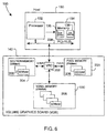
Figure 6 illustrates one embodiment of a volume rendering system 150 in
which a volume rendering pipeline such as the pipeline described with regard to
Figure 5A or 5B may be used to provide real-time interactive volume rendering.
In the embodiment of Figure 6, the rendering system 150 includes a host
computer 130 connected to a volume graphics board (VGB) 140 by an
interconnect bus 208. In one embodiment, an interconnect bus operating
according to a Peripheral Component Interconnect (PCI) protocol is used to
provide a 133 MHz communication path between the VGB 140 and the host
computer 130. Alternative interconnects available in the art may also be used
and the present invention is not limited to any particular interconnect.
-
The host computer 130 may be any sort of personal computer or
workstation having a comparable, i.e., PCI, bus interconnect. This bus can also
be called the host data path because it is used to transfer voxels between the
host memory and the voxel memory. Because the internal architectures of host
computers vary widely, only a subset of representative components of the host
130 are shown for purposes of explanation. In general, each host 130 includes a
processor 132 and a memory 134. In Figure 6 the memory 134 is meant to
represent any combination of internal and external storage available to the
processor 132, such as cache memory, DRAM, hard drive, and external zip or
tape drives.
-
In Figure 6, two components are shown stored in memory 134. These
components include a VGB driver 136 and a volume 138. The VGB driver 136
is executable program code that is used to control VGB 140. The volume 138 is
a data set represented as an array of voxels, such as that described with
reference to Figures 1-4, that is to be rendered on a display (not shown) by the
VGB 140. Each voxel in the array is described by its voxel position and voxel
value. The voxel position is a three-tuple (x,y,z) defining the coordinate of the
voxel in object space. Voxels may comprise 8-, 12- or 16-bit intensity values
with a number of different bit/nibble ordering formats. The present invention is
not limited to any particular voxel format.
-
Note that the formats specifying what is in host memory and what exists
in voxel memory are independent. Voxels are arranged consecutively in host
memory, starting with the volume origin, in permuted space, (x,y,z = 0,0,0).
Sizex, sizey, and sizez are the number of voxels in the host volume in each
direction, and thus, the voxel with "voxel coordinates" (x,y,z) has position p =
[x+ y*sizex + z*size*xsizey] in the array of voxels in host memory, where p is
the offset for voxel (x,y,z) from the volume origin.
-
During operation, portions of the volume 138 are transferred over the PCI
bus or host data path 208 to the VGB 140 for rendering. In particular, the voxel
data is transferred from the PCI-bus 208 to the voxel memory 100 by a Volume
Rendering Module (VRC) 202.
-
The VRC 202 includes all logic necessary for performing real-time
interactive volume rendering operations. In one embodiment, the VRC 202
includes N interconnected rendering pipelines such as those described with
regard to Figures 5A and 5B. Each processing cycle, N voxels are retrieved
from voxel memory 100 and processed in parallel in the VRC 202. By
processing N voxels in parallel, real-time interactive rendering data rates may
be achieved. A more detailed description of one embodiment of the VRC and its
operation are provided later herein.
-
In addition to voxel memory 100, the video graphics board (VGB) 140
also includes section memory 204 and pixel memory 200. Pixel memory 200
stores pixels of the image generated by the volume rendering process, and the
section memory 204 is used to store intermediate data generated during
rendering of the volume data set by the VRC 204. The memories 200, 202 and
204 include arrays of synchronous dynamic random-access memories
(SDRAMs) 206. As shown, the VRC 202 interfaces to buses V-Bus, P-Bus, and
S-Bus to communicate with the respective memories 200, 202 and 204. The
VRC 202 also has an interface for the industry-standard PCI bus 208, enabling
the volume graphics board to be used with a variety of common computer
systems.
-
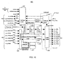
A block diagram of the VRC 202 is shown in Figure 7. The VRC 202
includes a pipelined processing element 210 having 4 parallel rendering
pipelines 212. Each pipeline may have processing stages coupled like those in
Figures 5A or 5B) and a render controller 214. The processing element 210
obtains voxel data from the voxel memory 100 via voxel memory interface
logic 216, and provides pixel data to the pixel memory 200 via pixel memory
interface logic 218. A section memory interface 220 is used to transfer read and
write data between the rendering engine 210 and the section memory 204 of
Figure 6. A PCI interface 222 and PCI interface controller 224 provide an
interface between the VRC 202 and the PCI bus 208. A command sequencer
226 synchronizes the operation of the processing element 210 and voxel
memory interface 216 to carry out operations specified by
commands received from the PCI bus. The data path along which the voxels
travel from the voxel memory to their destination pipelines are termed memory
channels.
-
The four pipelines 212-0- 212-3 operate in parallel in the x-direction, i.e.,
four voxels V(x0),y,z, V(x1),y,z, V(x2),y,z, V(x3),y,z are operated on concurrently at any
given stage in the four pipelines 212-0- 212-3. The voxels are supplied to the
pipelines 212-0-212-3, respectively via the memory channels, in 4-voxel groups
in a scanned order in a manner described below. All of the calculations for data
positions having a given x-coefficient modulo 4 are processed by the same
rendering pipeline. Thus it will be appreciated that to the extent intermediate
values are passed among processing stages within the pipelines 212-0 for
calculations in the y-and z-direction, these intermediate values are retained
within the rendering pipeline in which they are generated and used at the
appropriate time. Intermediate values for calculations in the x-direction are
passed from each pipeline (for example 212-0) to a neighboring pipeline (for
example, 212-1) at the appropriate time. The section memory interface 220 and
section memory 204 of Figure 6 are used to temporarily store intermediate data
results when processing a section of the volume data set 10, and to provide the
saved results to the pipelines when processing another section. Sectioning-related
operation is described in greater detail below.
Volume Rendering Data Flow
-
The rendering of volume data includes the following steps. First, the
volume data set is transferred from host memory 134 to the volume graphics
board 140 and stored in voxel memory 100. In one embodiment, voxels are
stored in voxel memory as mini-blocks. Each processing cycle, N voxels are
retrieved from voxel memory (where N corresponds to the number of parallel
pipelines in the VRC) and forwarded to corresponding ones of the N dedicated
pipelines.
-
The voxels are processed a section at the time, each section is processed a
slice at the time, and within slices by beams. Each of the pipelines buffers
voxels at a voxel, beam and slice granularity to ensure that the voxel data is
immediately available to the pipeline for performing interpolation or gradient
estimation calculations for neighboring voxels, received at different times at the
pipeline.
-
Data is transferred between different stages of the pipelines to like stages
of neighboring pipelines in only one direction. The output from the pipelines
comprises two-dimensional display data, which is stored in a pixel memory and
transferred to an associated graphics display card either directly or through the
host. Each of these steps is described in more detail below.
Sectioning a volume data set
-
In one embodiment, the volume data set is rendered a section at the time.
Figure 8 illustrates the manner in which the volume data set 10 is divided into
"sections" 340 for the purpose of rendering, in the x-direction. Each section 340
is defined by boundaries, which in the illustrated embodiment include
respective pairs of boundaries in the x-, y-and z-dimensions. In the case of the
illustrated x-dimension only sectioning, the top, bottom, front and rear
boundaries of each section 340 coincide with corresponding boundaries of the
volume data set 10 itself. Similarly, the left boundary of the left-most section
340-1 and the right boundary of the right-most section 340-8 coincide with the
left and right boundaries respectively of the volume data set 10. All the
remaining section boundaries are boundaries separating sections 340 from each
other.
-
In the illustrated embodiment, the data set 10 is, for example, 256 voxels
wide, in the x-direction. These 256 voxels are divided into eight sections 340,
each of which is exactly thirty-two voxels wide. Each section 340 is rendered
separately in order to reduce the amount of buffer memory required within the
processing element 210 because the size of buffers is proportional to the
number of voxels in a slice.
-
In the illustrated embodiment, the volume data set 10 may be arbitrarily
wide in the x-direction provided it is partitioned into sections of fixed width.
The size of the volume data set 10 in the y-direction is limited by the sizes of
the FIFO or delay buffers, such as buffers 106 and 114 of Figure 5A, and the
size of the volume data set 10 in the z-direction is limited by the size of a
section memory which is described below.
-
Note, however, that the limitations apply to permuted coordinates, as
such, for a different view direction, the limitations apply to different object axes.
Therefore, as a practical matter, the volume is cubic.
Transferring the Volume Data set from Host Memory to the VGB
-
Referring back again to Figure 6, in one embodiment, the transfer of
voxels between host memory 134 and voxel memory 100 is performed using a
Direct Memory Access (DMA) protocol. For example, voxels may be
transferred between host memory 134 and voxel memory 100 via the host data
path or PCI bus 208 with the VRC 202 as the bus master (for DMA transfers) or
the bus target.
-
There are generally four instances in which voxels are transferred from
host memory 134 to voxel memory 100 via DMA operations. First, an entire
volume object in host memory 134 may be loaded as a complete volume in
voxel memory 100. Second, an entire volume object in host memory 134 may
be stored as a subvolume in voxel memory 100, although this is an unlikely
event. A subvolume is some smaller part of an entire volume that normally
cannot be processed in one rendering pass. Third, a portion, or sub-volume of a
volume object in host memory 134 may be stored as a complete object in voxel
memory 100. Alternatively, a portion or subvolume of a volume object on the
host memory 134 is stored as a subvolume in voxel memory .
-
Transferring a complete volume from host memory 134 to voxel memory
100 may be performed using a single PCI bus master transfer, with the starting
location and the size of the volume data set specified for the transfer in a single
transfer command. To transfer a portion or subvolume of a volume data set in
host memory to voxel memory, a set of PCI bus master transfers are used,
because adjacent voxel beams of the host volume may not be stored
contiguously in the
host memory.
-
A number of registers are provided in the host and render controller 214
to control the DMA transfers between the host 130 and the VGB 140. These
registers include a Vx_HOST_MEM_ADDR register, for specifying the address
of the origin of the volume in host memory, a Vx_HOST_SIZE register for
indicating the size of the volume in host memory, a Vx_HOST_OFFSET
register, for indicating an offset from the origin at which the origin of a
subvolume is located, and a Vx_SUBVOLUME_SIZE register, describing the
size of the subvolume to be transferred. Registers Vx_OBJECT_BASE,
Vx_OBJECT_SIZE, Vx_OFFSET and Vx_SUBVOLUME_SIZE provide a
base address, size, offset from the base address and sub-volume size for
indicating where the object from host memory is to be loaded in voxel memory.
-
Transfers of rendered volume data set from voxel memory to the host
memory is performed using the registers described above and via DMA
transfers with the host memory 134 as the target.
Storing Voxels in Voxel Memory Mini-blocks
-
In one embodiment, voxel memory 100 is organized as a set of four
Synchronous Dynamic Random Access Memory modules (SDRAMs) operating
in parallel. Each module can include one or more memory chips. It should be
noted that more or less modules can be used, and that the number of modules is
independent of the number of pipelines. In this embodiment, 64 Mbit SDRAMs
with 16 bit wide data access paths may be used to provide burst mode access in a
range of, for example, 125-133 MHz. Thus, the four modules provide 256 Mbits
of voxel memory, sufficient to store a volume data set of 256x256x256 voxels at,
for example, sixteen bits per voxel. In one embodiment, voxel data is arranged as
mini-blocks in the voxel memory.
-
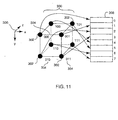
Figure 11 illustrates an array 300 of eight neighboring voxels 302
arranged in three-dimensional space according to the coordinate system of their
axes 306, here expressed in permuted object space. Note that in the examples
provide below, the conversion between the object coordinates (u,v,w) and the
permuted coordinate system (x,y,z), i.e., taking into account the view direction,
is done using a transform register. How the address translation occurs is
described in more detail later herein with reference to Figures 18-21 below.
-
The data values of the eight
voxels 300 are stored in an eight-
element
array 308 in one memory module of the
voxel memory 100. Each voxel
occupies a position in three-dimensional space denoted by coordinates (x, y, z),
where x, y, and x are all integers. The index of a voxel data value within the
memory array of its mini-block is determined from the lower order bit of each
of the three x, y, and z-coordinates. As illustrated in Figure 11, these three low-order
bits are concatenated to form a three-bit
binary number 304 ranging in
value from zero to seven, which is then utilized to identify the array element
corresponding to that voxel. In other words, the array index within a mini-block
of the data value of a voxel at coordinates (x, y, z) is given by Equation II:
-
Just as the position of each voxel or sample can be represented in three
dimensional space by coordinates (x, y, z), so can the position of a mini-block
be represented be represented in mini-block coordinates (x
mb , y
mb , z
mb ). In these
coordinates,
xmb represents the position of the mini-block along the
x-axis,
counting in units of whole mini-blocks. Similarly, y
mb and z
mb represent the
position of the mini-block along the y-and z-axes, respectively, counting in
whole mini-blocks. Using this notation of mini-block coordinates, the position
of the mini-block containing a voxel with coordinates (x, y, z) is given by
Equation III:
-
In one embodiment of the invention, mini-blocks are skewed such that
consecutive mini-blocks in the volume data set, in either the x, y, or z-dimension,
are stored in different ones of the four SDRAM modules of the
voxel memory. Referring now to Figure 12, the first level of mini-block
skewing is illustrated. The DRAM number of a mini-block having voxel
coordinates of (x,y,z) is provided below in Equation IV:
-
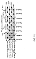
In Figure 12, a partial view of a three-dimensional array of mini-blocks
300 is illustrated. Each mini-block is depicted by a small cube labeled with a
small numeral. The numeral represents the assignment of that mini-block to a
particular DRAM module. In the illustrated embodiment, there are four different
DRAM modules labeled 0, 1, 2, and 3. It will be appreciated from the figure
that each group of four mini-blocks aligned with an axis contains one mini-block
with each of the four labels.
-
This can be confirmed from Equation IV. That is, starting with any mini-block
at coordinates (x mb , y mb , z mb ), and sequencing through the mini-blocks in
the direction of the x-axis, the DRAMNumber of Equation IV cycles continually
through the numbers 0, 1, 2, and 3. Likewise, by sequencing through the mini-blocks
parallel to the y-or z-axis, Equation IV also cycles continually through
the DRAMNumbers 0, 1, 2, and 3. Therefore, it will be appreciated that when
traversing the three-dimensional array of mini-blocks in any direction 309, 311, or
313 parallel to any of the three axes, groups of four adjacent mini-blocks can
always be fetched in parallel from the four independent memory of the DRAM
modules. The assignment of mini-blocks to memory locations within a memory
module is discussed below.
-
More generally, if a system contains
M independent memory modules,
then the mini-block with coordinates (x
mb , y
mb , z
mb ) is assigned to a memory
module as indicated by Equation V below:
-
That is, if the memory subsystem of the illustrated embodiment comprises
M separate modules such that all M can be accessed concurrently in the same
amount of time required to access one module to achieve parallelism, then the
assignment of a mini-block to a memory module is given by summing the
coordinates of the mini-block, dividing by M and taking the remainder.
-
This guarantees that any group of M blocks aligned with any axis can be
fetched concurrently. It will be appreciated that the requirement for fetching
groups of M mini-blocks concurrently along any axis of the volume data set is
because order of traversal of the volume data set is dependent upon the view
direction.
-
Although in the illustrated embodiment, mini-blocks are accessed in linear
groups aligned with the axes of the volume data set, it will be appreciated that
other embodiments may skew mini-blocks by different formulas so that they can
be fetched in rectangular groups, cubic groups, or groups of other size and shape,
independent of the order of traversal of the volume data set.
Organization into Banks of Memory
-
In modern DRAM modules, it is possible to fetch data from or write data
to the DRAM module in "bursts" of modest size at the clock rate for the type of
DRAM. Typical clock rates for Synchronous DRAM or "SDRAM" modules
include 133 MHz, 147 MHz, and 166 MHz, corresponding 7.5 nanoseconds, 7
nanoseconds, and 6 nanoseconds per cycle, respectively.
-
Typical burst sizes needed to sustain the clock rate are five to eight
memory elements of sixteen bits each. Other types of DRAM under
development have clock rates up to 800 MHz and have typical burst sizes of
sixteen data elements of sixteen bits each. In these modern DRAM modules,
consecutive bursts can be accommodated without intervening idle cycles,
provided that they are from independent memory banks within the DRAM
module. That is, groups of consecutively addressed data elements are stored in
different or non-conflicting memory banks of a DRAM module, then they can
be read or written in rapid succession, without any intervening idle cycles, at
the maximum rated speed of the DRAM.
-
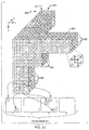
Referring now to Figure 13, the mini-blocks are further arranged in
groups corresponding to banks of the DRAMs. This constitutes the second level
of voxel skewing. Each group of 4×4×4 mini-blocks is labeled with a large
numeral. Each numeral depicts the assignment of each mini-block of that group
to the bank with the same numeral in its assigned DRAM module. For example,
the group of mini-blocks 312 in the figure is labeled with numeral 0. This
means that each mini-block within group 312 is stored in bank 0 of its
respective memory module. Likewise, all of the mini-blocks of group 314 are
stored in bank 1 of their respective memory modules, and all of the mini-blocks
of group 316 are stored in bank 2 of their respective memory modules.
-
In the illustrated embodiment, each DRAM module has four banks,
labeled 0, 1, 2, and 3. A mini-block with coordinates (
xmb, ymb, zmb ) is assigned to
the bank according to Equation VI below:
The fact that the number of banks per DRAM module is the same as the number
of DRAM modules in the illustrated embodiment is a coincidence. Other
embodiments can have more or less module modules, and each module can
have more or less banks.
-
It will be appreciated from the figure that when a set of pipelined
processing elements traverses the volume data set in any given orthogonal
direction, fetching four mini-blocks at a time in groups parallel to any axis,
adjacent groups, such as Group 0 and Group 1, are always in different banks.
This means that groups of four mini-blocks can be fetched in rapid succession,
taking advantage of the "burst mode" access of the DRAM modules, and
without intervening idle cycles on the part of the DRAM modules, for traversal
along any axis. This maximizes the efficiency of the DRAM bandwidth.
-
More generally, the assignment of mini-blocks to memory banks can be
skewed in a way similar to the assignment of mini-blocks to memory modules.
In other words, mini-blocks can be skewed across
M memory modules so that
concurrent access is possible no matter which direction the volume data set is
being traversed. Likewise, mini-blocks within each module can be skewed
across
B memory banks, so that accesses to consecutive mini-blocks within a
bank are not delayed by intervening idle cycles. This forms a two-level skewing
of mini-blocks across modules and banks. In the illustrated embodiment, the
assignment of a mini-block to a memory bank is given by Equation VII below:
-
It will be appreciated, however, that other embodiments may skew mini-blocks
across banks by other rules, for example by skewing in each dimension by
a different distance such that the distances in the three dimensions are relatively
prime to each other.
Traversal of the Volume during Rendering
-
Although the voxels are arranged in voxel memory as mini-blocks, they are
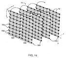
processed in a slice/beam order. Referring now to Figure 14, a description of
what is meant by slice/beam order is provided. As described above with
reference to Figure 8, the volume data set 10 is processed as parallel "slices"
330 in the z-direction, which as described above is the axis most nearly parallel
to the view direction. Each slice 330 is divided into "beams" 332 in the y-direction,
and each beam 332 consists of a row of voxels 12 in the x-direction.
The voxels 12 within a beam 332 are divided into groups 334 of voxels 12
which as described above are processed in parallel by the four rendering
pipelines 212.
-
In the illustrative example, the groups 334 consist of four voxels along a
line in the x-dimension. The groups 334 are processed in left-to-right order
within a beam 332; beams 332 are processed in top-to-bottom order within a
slice 330; and slices 330 are processed in order front-to-back. This order of
processing corresponds to a three-dimensional scan of the data set 10 in the x, y,
and z-directions. It will be appreciated that the location of the origin and the
directions of the x, y, and z-axes can be different for different view directions.
-
Although in Figure 14, the groups 334 are illustrated as linear arrays
parallel to the x-axis, in other embodiments the groups 334 may be linear arrays
parallel to another axis, or rectangular arrays aligned with any two axes, or
parallelepipeds. Beams 332 and slices 330 in such other embodiments have
correspondingly different thicknesses. For example, in an embodiment in which
each group 334 is a 2x2x2 rectangular mini-block, the beams 332 are two
voxels thick in both the y-and z-dimensions, and the slices 330 are 2 voxels
thick in the z-dimension. The method of processing the volume data set
described herein also applies to such groupings of voxels.
Voxel Memory Interface
-
The writing of voxels to voxel memory 100 in skewed mini-block format
and the processing of voxels in a slice/beam order by the pipelines is controlled
by the voxel memory interface 216 (Figure 7). The memory interface is part of
the memory-to-pipeline memory channel. A block diagram of one embodiment
of the voxel memory interface 216 (VxIf) is showing in Figure 15. As illustrated
in Figure 6, the voxel memory is located between the rendering pipelines of
VRC 202 and voxel memory 100.
-
The voxel memory interface 216 controls the reading of voxels from
voxel memory and the rearrangement of the voxels so that they are presented to
the rendering pipelines in the correct order for rendering. The data sent to the
pipelines via the memory channels includes voxel data from two adjacent slices,
z-gradients corresponding to those slices, and control information. The VxIf
also includes an interface to the PCI controller in the VRC 202, and the VxIf
implements read and write cycles initiated by host-to-voxel memory traffic.
-
The VxIf 216 includes a memory interface 400, a traverser 402, a weight
generator 404, a deskewer (VxDeskew) 408, a slice buffer (VxSliceBuffer) 410,
an output unit (VxSbOutput) 412 and a controller (VxSbCntrl) 406.
-
The memory interface 400 includes four memory interfaces, one for each
of the four respective SDRAM modules of voxel memory. The fact that the
number of modules and the number of pipelines are the same is purely
coincidental. The weight generator 404 computes weights that represent the
offset, from the voxel grid, of the rays as they pass through a particular slice of
voxels. The deskewer 408 rearranges the skewed order of voxels received from
banks of SDRAM of voxel memory so that the eight voxels are ordered in mini-block
order. The traverser 402 controls the order in which addresses are
dispatched to the voxel memory. The slice buffer 410 includes a number of
buffers that are used to temporarily store data retrieved from voxel memory,
and to rearrange the voxels from mini-block order to the appropriate beam/slice
order. The output unit 412 and controller 406 forward voxel data from the voxel
memory interface to the rendering pipelines 212a-212d. The memory interfaces
411a-411d, traverser 402, deskewer 408 and slice buffer 410 which form the
operative part of the memory channels are described in more detail below.
Memory Controller
-
Referring now briefly to Figure 16, a block diagram of one embodiment
of a memory controller 400 is shown. The memory controller 400 includes a
host datapath 403 for transferring address, control and data, received from the
host via the PCI data bus 208 and the VRC 202, respectively, to voxel memory
100. Thus, this datapath is used to forward data to the voxel memory from host
memory. The PCI interface requests reads or write cycles to voxel memory
through pc_vxRequest signal 403a, pc_vxMemReg signal 403c and
pc_vx_ReadWrite signal 403b. An access is made to voxel memory when
pc_vxMemReg and pc_vx_Request are both high. The lines pf the host path 403
are coupled to each individual memory interfaces 411a-d. The memory
controller decodes addresses provided on pc_vxAddress bus 403d and
pc_vxByteEn 403f.
-
Address, data and control signals are forwarded to VxResidue 425 from
the VRC 202. In addition, a stall signal vx_pcStall is held in the register 425.
The register is used to provide an extra stage of logic before the stall signal is
forwarded to the VRC 202. The VxResidue circuit 425 contains logic needed to
be able to align write data for unaligned access. Addresses and data and control
from the PCI interface are also be forwarded to VxSetup registers 427.
-
VxSetup registers 427 include a number of front end registers that are
used for rendering an object. These registers include the following:
RENDER_OBJECT_SIZE, RENDER_OBJECT_BASE, Vx_OBJECT_SIZE,
Vx_OBJECT_BASE, transform, leftx, lefty, topy, bottomy, frontz, backz,
leftSection and rightSection among others. In one embodiment, the registers are
all write-only and for each register there are two sets of storage, active and
pending. The various uses of the contents of each of these registers is described
in more detail below.
-
The PCI address is forwarded to VxAddrMux 432 which operates as an
address selector. The VxAddrMux 432 selects between the PCI address (which
is used during initial write operations) and an address provided by the traverser
402 (Fig. 16). The traverser 402, as will be described in more detail below,
provides successive addresses starting at an origin address and incrementing
along a given plane. Thus, the traverser is an automatic address generator that is
used to read voxels from voxel memory in bursts of eight.
-
The selected address is then forwarded to a multiplier (VxAddrMult 435)
and an address translator (VxAddrTrans 442). The addresses received from both
the traverser and the PCI interface are logical addresses provided in x,y,z
coordinates, where x,y, and z are three-dimensional coordinates voxels of a
volume stored in host memory having an origin (x,y,z) = (0,0,0). The addresses
received from the traverser are already mini-block relative. However, the
addresses received from the PCI interface are voxel relative.
-
To compute the physical address in voxel memory from the x, y-and z-coordinates
provided from the multiplexer 432, when the coordinates are
provided by the PCI interface, the coordinates are converted to mini-block
coordinates xmb, ymb, zmb by removing the least significant bit from each of the
coordinate. Once the mini-block relative coordinates are ascertained (whether
they be from the traverser or from the PCI interface), the SDRAM address is
then determined by the VxAddrMult 435 and the VxAddrTrans 442 as follows.
The SDRAM number is determined using above Equation V. The bank address
of the SDRAM associated with the mini-block is determined using above
Equation VII.
-
The row address within the bank is determined using below Equations
VIIIa - VIIIc:
Relative row address = (xmb + ymb*Sizex + zmb * Sizex*Sizey),
where Sizex is the number of mini-blocks in the x-plane and Sizey is the
number of mini-blocks in the y-plane. In one embodiment, wherein the volume
is a parallelepiped with the Sizex = Size y = Sizez, the size of the volume in
each dimension is stored in a register Vx_OBJECT_SIZE (if the address is from
the PCI interface) or a register RENDER_OBJECT_SIZE (if the address is
from the traverser) in the setup registers 427 of memory interfaces 411a-411d.
Absolute row address = relative row + base offset,
where the base offset is stored in either a register Vx_OBJECT_BASE (if the
address is from the PCI interface) or a register RENDER_OBJECT_BASE (if
the address is from the traverser) in the setup registers 427 of the memory
interfaces 411a-411d.
Row address to SDRAMs = absolute row/512,
where the 512 is dependent on the row size of a particular SDRAM. This divide
computation can easily be done by a shift of (nine) bit positions.
-
The column addresses are generated as follows. For reads, when the
address is provided from the traverser, since accesses are always made in bursts
of eight reads, the lower three bits of the column address are zero. For writes,
when the address is from the PCI interface, the lower order bits of the column
address are determined as shown below in Equation IX:
Column [2] = z[0], column[1] = y[0], column[0] = x[0]
The remaining bits of the column address are determined according to Equation
X below:
column (7:3) = row(8:4)
-
The address, whether from the traverser or from the PCI interface, is
forwarded to the voxel controller state machine (VxMiState) 450. The voxel
controller state machine 450 operates in response to the address received from
the VxAddrTrans 442 and the requests received from the VxMemCntrl 430 to
properly assert control signals 401 of the SDRAMs to performs reads, writes
and refreshes of the voxel memory. Write data is forwarded to the voxel
memory on line 401d, while read data is obtained from voxel memory on line
401e. Received data is collected in the controller at VxBuildLatch 444.
-
There are two output ports from the memory controller. The first output
port is to the PCI interface, and thus data is forwarded on lines 403h- 403j to the
PCI interface in the VRC 202. The second output port is to the deskewer 408.
Data is forwarded from the build latch to the deskewer 408 for later forwarding
to the rendering pipeline (after storage in the slice buffers) as will be described
later herein.
Voxel Memory State Machine
-
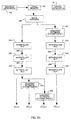
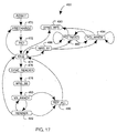
Referring now briefly to Figure 17, a state diagram of the voxel state
machine 450 will first be described. The state machine 450 receives and
processes requests from the different sources of voxel memory traffic and issues
specific commands to the different independent memory interfaces. The
requests include render requests, read and write requests, and maintenance
requests. The render requests synchronously transfers voxels from the memory
modules to the rendering pipelines. The read and write requests asynchronously
transfer data between the host and voxel memories. The maintenance requests
refresh and precharge the memories.
-
The order in which the requests are processed is based on a priority of the
request, from highest to lowest and in the following order: power up sequence
at start up only, and while the system is operational, render request,
maintenance request and read/write requests. Thus, rendering is the highest
priority task during operation, and will always take precedence over
maintenance requests, and read or write requests.
-
As shown in Figure 17, after a reset, the state machine proceeds to
PRECHARGE state 470, where the row and column lines of the SDRAMs are
precharged in a standard SDRAM precharge cycle. The state machine then
proceeds to REF state 472, where a refresh cycle is performed.
-
The state machine then proceeds to IDLE state 474, wherein it remains
until either a time-out causes the state machine to return to the PRECHARGE
state 470, or until the state machine receives a request.
-
If the request is a read or write request, then the state machine proceeds
to state MRS_B1 488, where a BURST_MODE register is written to a value of
one, and the request is decoded. The PCI_READ state 492 performs the read,
and the PCI_WRITE state 494 the write. The state machine remains in this
states until all data is returned, and then proceeds to state SYNC_RFS 490, and
then PRECHARGE 470.
-
If a render request is received, then the state machine proceeds to
SYNC_RENDER state 476. In the SYNC_RENDER state, the state machine
waits until all memory interfaces are idle, and then proceeds to MRS_B8 state
478, where the BURST_MODE register is written with the value of eight. The
state machines then proceeds to Vx_READY state 480.
-
In Vx_READY state 480, the circuit is ready to render and the state
machine proceeds to RENDER state 482. At RENDER state 482, the
appropriate signals are forwarded to the SDRAM to perform a burst mode read
of eight voxels, and the state machine returns to Vx_READY state 480. The
state machine stays in the Vx_READY state 480 until the burst mode read has
completed, and, if there is more to read, then the state machine cycles between
states 482 and 480 until the entire render request has been completed.
-
When the render request has been completed, the state machine proceeds
from Vx_READY state 480 to REF_ALL state 486, where all of voxel memory
is refreshed. The state machine then returns to IDLE state 474, where it awaits
receipt of a next request or a precharge cycle.
-
Thus, the state machine provides a mechanism for handling both PCI
reads and write and burst mode render operations, while supporting refresh and
precharge requirements of the SDRAMs.
-
By giving priority to render requests over PCI read and write requests,
the state machine can assure that real-time rendering rates are maintained.
-
Referring back to Figure 15, some of the remaining components of the
voxel memory interface will now be described.
Transformation of Coordinates
-
The traverser 402 is responsible for providing addresses associated with
render requests of mini-blocks to the voxel memory interface 400 in the correct
order based on the view direction. According to one embodiment of the
invention, the traverser uses a transform register 520, see Figure 19, to
transform the addresses of the voxel element from the object coordinate system
into addresses of voxels in the permuted coordinate system, that is where the
volume has been repositioned according to the view direction. Performing this
translation at the memory interfaces provides an easy method of changing views
of the volume without having to actually alter the contents of memory.
-
Referring now to Figure 18, a block diagram of one embodiment of the
traverser 402 is shown to include counters 500 and address generation logic 502.
The counters 500 generate mini-block coordinates for the leftmost mini-block
of a partial mini-block beam. While the counters hold object coordinates in
(u,v,w) space, they are incremented or decremented as they traverse an object in
x,y,z order. This performs part of the transformation from object (u,v,w) space
(where the origin of a volume is located at one corner of the volume, typically a
starting point from the object's own point of view) to a permuted (x,y,z) space
(where the origin of the object is repositioned to be the vertex of the volume
nearest to the image plane, and the z-axis is the edge of the volume most nearly
parallel to the view direction).
-
The traversal order follows the x, then y, then z, then section order. The u,
v, and w coordinates are loaded into the x, y-and z-counters based on the
chosen view direction and the mappings selected in the transform register 520
of the memory controller. The transform register is used to transform the
addresses of the volume data set depending upon the view direction. Thus, the
transform register may be used to convert the logical origin of the volume from
object to permuted coordinates.
-
Figure 19 shows exemplary mapping data stored in the transform register
520. The mapping data, which maps between the object coordinate system and
the permuted coordinate system as shown in Figure 1, includes selectx field 522,
selecty field 523 and selectz field 524. Using the selectx, selecty and selectz
fields, the u coordinate can be mapped to x, y-or z-plane, as can the v and w
coordinates. In addition, transform matrix includes negx field 526, negy field
527 and negz field 528. Fields 526-528 are used to provide an increment count
for the counters of each of the respective x, y-and z-dimensions. In essence, the
voxels in the volume may be rotated or flipped in any of the three dimensions
based on the contents of the transform register 520.
-
Referring back to Figure 18, the counters 500 of the traverser 402 include
a count to eight counter 500a, an x-dimension counter 500b, a y-dimension
counter 500c, a z-dimension counter 500d and a section counter 500e.
-
As mentioned above, the increment value for each of the counters are
based upon the negx, negy and negz fields of the transform register 520. For
example, if the field of negx is set to a one, the increment value would be a-1,
otherwise it would be a +1.
-
The leftX, leftX, righty, bottomy, frontZ, backZ and leftSection,
rightSection values from the Setup registers 427 define the voxel coordinates of
the volume data set in voxel memory. These values are used to compute initial
and final values for each of the counters as mini-block addresses. During each
cycle in one embodiment, partial mini-block "beam" units (comprising four
mini-blocks) are forwarded to the address generator 502. The address generator
502 converts the partial mini-block beam coordinates into four distinct mini-block
addresses for each of the mini-blocks in the beam. These four addresses
point to four corresponding mini-blocks in each of the four SDRAMs. Using
these coordinates, the address generator forwards addresses to each of the four
memory modules to retrieve the mini-blocks.
Deskewer
-
Each mini-block is read as a set of consecutive memory addresses from its
memory module and bank using the addresses generated by the traverser. It will
be appreciated that, because of the skewing of mini-blocks during the write
process (described above with regard to Equations II-VIII), the order of voxel
values provided in a mini-block read does not necessarily correspond to the order
in which voxels are processed. To take account for this situation, a method of deskewing
using a deskewer is introduced as follows.
-
Each read cycle of the four SDRAMs provides thirty-two voxels in bursts
of eight, the deskewer receives four mini-blocks of data in each burst read cycle.
-
The order of the received voxels for each of the four mini-blocks is
deskewed using a circuit such as that shown in Figure 20. The deskewer 408 is
shown to include a sequence of buffers 444, one for each of the M SDRAM
devices (where in the present embodiment, four SDRAM devices are provided).
Multiplexers 438 are provided to re-arrange the order of received voxels to reflect
an expected order of voxels (1-8 as shown in Figure 11).
-
The selection of the voxel is controlled by mini-block deskew logic 440 via
line 442. The mini-blocks are then forwarded to the VxSliceBuffer 410.
-
The deskew logic 440 rearranges the order of the received voxels to an
expected order of voxels (1-8 as shown in Figure 11) in response to the amount of
skewing that was performed during the write of voxels to voxel memory and
further in response to the contents of transform register 520. In general, the
rearrangement of the order of voxels follows six rules.
-
If the transform register indicates to exchange x and y, then the voxel in
position 1 is swapped with that in position 2, and the voxel in position 5 is
swapped with the voxel in position 6. If the transform register indicates to
exchange x and z, then the voxel in position 1 is swapped with the voxel in
position 4, and the voxel in position 3 is swapped with the voxel in position 6. If
the transform register indicates to exchange y and z, then the voxel in position 2 is
exchanged with the voxel in position 3 and the voxel in position 4 is exchanged
with the voxel in position 5.
-
If the transform register indicates to negate x, then voxels in successive
even and odd locations are exchanged (i.e., voxel 0 with 1, 2 with 3, etc). If the
transform register indicates to negate y, then voxels 0 and 1 are exchanged with
voxels 2 and 3 and voxels 4 and 5 are exchanged with voxels 6 and 7. If the
transform register indicates to negate z, then voxels in the positions 0,1,2 and 3
are exchanged with voxels in the positions 4,5,6 and 7.
-
In determining which module is the starting module, the following rules are
used. If the sign of x is negative, then decrement from the starting module, else
increment. If each of the sign of x, sign of y, sign of z is positive, then the starting
module is 0. If two of the group including sign of x, the sign of y and sign of z are
negative, and one is positive, then the starting module is 2. If two of the group
including sign of x, the sign of y, and the sign of z are positive, and one is
negative, then the starting module is three. If all of the group of sign of z, sign of y
and sign of z are negative, then the starting module is 1.
-
Referring to Figure 21, a table 525 illustrates example voxel orders based
on the contents of the transformation register 520. Using the above rules, the
deskewer logic 440 appropriately re-arranges the order of the voxels such that the
voxels are ordered in expected mini-block order for processing.
Slice Buffers
-
As described above, after the voxels have been deskewed, a mini-beam of
four mini-blocks is forwarded to the vxSliceBuffer 410. The slice buffers provide
storage so that voxels received in mini-beam orientation can be converted to slice
orientation for forwarding to the processing pipelines.
-
Figure 22 illustrates the relationship between voxels in mini-beam
orientation and slice orientation. Mini-block 370, received from the deskewer
410, includes voxels a-h. In one embodiment the slice buffers are apportioned
into even and odd pairs, each pair associated with data stored at consecutive
even and odd slices of the volume data set. Each cycle that incoming voxel data
is valid, sixteen voxels are written into the slice buffer, with eight voxels
associated with a given (y, z) to one of the even numbered slice buffers N, i.e.,
voxels a and b of each of mini-blocks 370, 372, 374 and 376, and eight voxels
associated with (y, z+1) to the next odd slice buffer N+1 i.e., the voxels c and d
of each of the mini-blocks 370-376.
-
The next cycle, sixteen more voxels, representing voxels c and f of
blocks 370-376 and voxels g-h of blocks 370-376, respectively, are written to
the same two slice buffers. The writing to these two buffers continues until the
slice is completed, then the next mini-beam received from the deskewer 410 is
written as described above to slice buffer pair N+2 and N+3.
-
Referring now to Figure 23A, a block diagram illustrating one
embodiment of the VxSliceBuffer 410 and the VxSbOutput 412 logic is
provided. VxSliceBuffer 410 includes six slice buffer memories, each storing
one slice worth of voxel data (i.e., 32 x 256 x 12 bits). In one embodiment, each
slice buffer is formed from a 1K x 96 memory device, which is capable of
storing eight 12-bit voxels in a given write cycle. Slice buffers 530, 534 and
538 are even slice buffers, and the slice buffers 532, 536 and 540 are odd slice
buffers. Using the example of Figure 22, and assuming that the mini-blocks are
from slice 0 and 1 of the volume data set, a first beam of voxels, such as beam
380 is written to even slice buffer 530 at the same time as a second beam of
voxels, such as beam 382 is written to odd slice buffer 532.
-
In the next write cycle, beam 384 is written to slice buffer 530 while
beam 386 is written to slice buffer 532. The writing of mini-blocks to the two
slice buffers until the entire section for slice 0 and slice 1 has been stored in the
slice buffers 530 and 532. Section data for slice 3 and slice 4 are stored in slice
buffers 534 and 536 and section data for slice 5 and 6 are stored in slice buffer
538 and 540. This sequence of slice buffer even and odd pair writes continues
for each of the following slices of the volume data set.
-
Once sufficient data has been written into the slice buffers the rendering
process may begin. In order to perform the rendering process, voxels are
forwarded from the slice buffers to the associated pipelines. The VxSbOutput
412 controls the forwarding of data to the associated pipelines. The
VxSbOutput 412 includes a selector 550. The selector is coupled to the output
of the six slice buffers 530-540, and selects four of the six values to use to
generate data to forward to the rendering pipelines.
Rendering Pipelines
-
Figure 9 shows the processing element 210 of Figure 7, including four
processing pipelines 212 similar to those described in Figures 5A and 5B.
Parallel pipelines 212 receive voxels from voxel memory 100 and provide
accumulated rays to pixel memory 200. For clarity only three pipelines 212-0,
212-1 and 212-3 are shown in Figure 14.
-
As described previously in Figures 5A and 5B, each pipeline 212
includes an interpolation unit 104, a gradient estimation unit 112, a
classification unit 120, an illumination unit 122, modulation units 126 and a
compositing unit 124, along with associated FIFO buffers and shift registers.
Each pipeline processes adjacent voxel of sample values in the x-direction. That
is, each pipeline processes all voxels 12 whose x-coordinate value modulo 4 is a
given value between 0 and 3. Thus for example pipeline 212-0 processes voxels
at positions (0,y,z), (4,y,z), ... , (252,y,z) for all y and z between 0 and 255.
Similarly, pipeline 212-1 processes voxels at positions (1,y,z), (5,y,z), ... ,
(253,y,z) for all y and z, etc.
-
In order to time-align values needed for calculations, each operational
unit or stage of each pipeline passes intermediate values to itself in the y- and z-dimensions
via the associated FIFO buffers. For example, each interpolation
unit 104 retrieves voxels at positions (x,y,z) and (x,y+1,z) in order to calculate
the y-component of an interpolated sample at position (x,y,z).
-
The voxel at position (x,y,z) is delayed by a beam FIFO 108 (see Figure
5A) in order to become time-aligned with the voxel at position (x,y+1,z) for this
calculation. An analogous delay can be used in the z-direction in order to
calculate z-components, and similar delays are also used by the gradient units
112 and compositing units 124.
-
It is also necessary to pass intermediate values for calculations in the x-direction.
However, in this case, the intermediate values are not merely delayed
but are also transferred out of one pipeline to a neighboring pipeline. Each
pipeline (such as pipeline 212-1) is coupled to its neighboring pipelines (i.e.,
pipelines 212-0 and 212-2) by means of shift registers in each of the four
processing stages (interpolation, gradient estimation, classification and
compositing). The shift registers are used to pass processed values from one
pipeline to the neighboring pipeline. In one embodiment, the final pipeline,
pipeline 212-3, transfers data from shift registers 110, 118 and 250 to section
memory 204 for storage. This data is later retrieved from section memory 204
for use by the first pipeline stage 212-0. In essence, voxel and sample values are
circulated among the pipelines and section memory so that the values needed
for processing are available at the respective pipeline at the appropriate time
during voxel and sample processing.
-
Because voxels are forwarded to the pipelines in slice/beam order, rather
than as mini-blocks, the amount of data stored by any individual pipeline is
reduced. In addition, the reduction in the amount of data retrieved each cycle
further reduces the amount of data that needs to be transferred between various
stages of the pipeline. Because less data is stored and transferred between
pipelines, the multiple pipelines may be fabricated on a single integrated circuit
device. Thus, a low-cost alternative is provided to implement real-time
interactive volume rendering.
-
Accordingly, a volume data memory architecture has been
introduced that makes optimum use of memory components by strategically
writing voxels in memory in a skewed mini-block format that allows retrieval
of the voxels in burst mode. Retrieving the voxels in burst mode allows the full
performance potential of the memory devices to be realized, thereby facilitating
real-time interactive rendering. In one embodiment, volume coordinates are
stored as object coordinates, and translated by the memory interface into
permuted coordinates to align the rendered components with a view direction. A
transform register may be used to transform the addresses of the voxel element
into addresses of voxels having the desired view. Performing this translation at
the memory interfaces provides an easy method of changing views of the
volume without having to actually alter the contents of memory.
-
The memory is controlled by a state machine which prioritizes render
requests over other types of operations so that real-time rendering may be more
easily achieved. Voxels retrieved as a result of a render request are then
rearranged into a second format by voxel memory interface logic before being
forwarded to pipelines for rendering. The second format is selected such that the
amount of data that need be stored by each of the rendering pipelines and
passed between the pipelines may be minimized, thereby making it possible to
provide real-time interactive rendering capabilities within one integrated circuit.
-
Having now described a few embodiments of the invention and some
modifications and variations thereto, it should be apparent to those skilled in the
art that the foregoing is merely illustrative and not limiting, having been
presented by way of example only. Numerous modifications and other
embodiments are within the scope of one of ordinary skill in the art and are
contemplated as falling within the scope of the invention as defined by the
appended claims and equivalents thereto.