EP1052726A1 - Slot coupled micromachined waveguide antenna - Google Patents
Slot coupled micromachined waveguide antenna Download PDFInfo
- Publication number
- EP1052726A1 EP1052726A1 EP00870097A EP00870097A EP1052726A1 EP 1052726 A1 EP1052726 A1 EP 1052726A1 EP 00870097 A EP00870097 A EP 00870097A EP 00870097 A EP00870097 A EP 00870097A EP 1052726 A1 EP1052726 A1 EP 1052726A1
- Authority
- EP
- European Patent Office
- Prior art keywords
- substrate
- layer
- insulating layer
- cavity
- metallic layer
- Prior art date
- Legal status (The legal status is an assumption and is not a legal conclusion. Google has not performed a legal analysis and makes no representation as to the accuracy of the status listed.)
- Granted
Links
- 239000000758 substrate Substances 0.000 claims abstract description 62
- 238000000034 method Methods 0.000 claims description 37
- 238000004519 manufacturing process Methods 0.000 claims description 14
- 229920000642 polymer Polymers 0.000 claims description 13
- 238000000151 deposition Methods 0.000 claims description 8
- 239000002861 polymer material Substances 0.000 claims description 6
- 239000004033 plastic Substances 0.000 claims description 5
- 229920003023 plastic Polymers 0.000 claims description 5
- 238000011049 filling Methods 0.000 claims description 4
- 230000005855 radiation Effects 0.000 claims description 4
- 239000004065 semiconductor Substances 0.000 claims description 3
- 229910010293 ceramic material Inorganic materials 0.000 claims 1
- 239000010410 layer Substances 0.000 description 54
- 239000000463 material Substances 0.000 description 16
- 238000005516 engineering process Methods 0.000 description 14
- XUIMIQQOPSSXEZ-UHFFFAOYSA-N Silicon Chemical compound [Si] XUIMIQQOPSSXEZ-UHFFFAOYSA-N 0.000 description 13
- 235000012431 wafers Nutrition 0.000 description 13
- 229910052710 silicon Inorganic materials 0.000 description 12
- 239000010703 silicon Substances 0.000 description 12
- 238000004891 communication Methods 0.000 description 9
- 230000008878 coupling Effects 0.000 description 7
- 238000010168 coupling process Methods 0.000 description 7
- 238000005859 coupling reaction Methods 0.000 description 7
- 230000010354 integration Effects 0.000 description 6
- 239000002184 metal Substances 0.000 description 6
- 229910052751 metal Inorganic materials 0.000 description 6
- 229910000577 Silicon-germanium Inorganic materials 0.000 description 5
- 239000000919 ceramic Substances 0.000 description 5
- 229910001218 Gallium arsenide Inorganic materials 0.000 description 4
- 230000005540 biological transmission Effects 0.000 description 4
- 229910052802 copper Inorganic materials 0.000 description 4
- 239000010949 copper Substances 0.000 description 4
- 238000011161 development Methods 0.000 description 4
- 230000018109 developmental process Effects 0.000 description 4
- RYGMFSIKBFXOCR-UHFFFAOYSA-N Copper Chemical compound [Cu] RYGMFSIKBFXOCR-UHFFFAOYSA-N 0.000 description 3
- 238000013461 design Methods 0.000 description 3
- 238000005459 micromachining Methods 0.000 description 3
- 238000001053 micromoulding Methods 0.000 description 3
- 238000000465 moulding Methods 0.000 description 3
- 229920003229 poly(methyl methacrylate) Polymers 0.000 description 3
- 239000004926 polymethyl methacrylate Substances 0.000 description 3
- CSCPPACGZOOCGX-UHFFFAOYSA-N Acetone Chemical compound CC(C)=O CSCPPACGZOOCGX-UHFFFAOYSA-N 0.000 description 2
- 229930040373 Paraformaldehyde Natural products 0.000 description 2
- 239000004952 Polyamide Substances 0.000 description 2
- 238000003491 array Methods 0.000 description 2
- 239000003989 dielectric material Substances 0.000 description 2
- 238000001312 dry etching Methods 0.000 description 2
- 238000010304 firing Methods 0.000 description 2
- 238000001746 injection moulding Methods 0.000 description 2
- 239000012528 membrane Substances 0.000 description 2
- 238000000206 photolithography Methods 0.000 description 2
- 229920002647 polyamide Polymers 0.000 description 2
- 229920006324 polyoxymethylene Polymers 0.000 description 2
- 238000012545 processing Methods 0.000 description 2
- 230000001902 propagating effect Effects 0.000 description 2
- 239000011241 protective layer Substances 0.000 description 2
- 238000010107 reaction injection moulding Methods 0.000 description 2
- 230000010076 replication Effects 0.000 description 2
- 239000011347 resin Substances 0.000 description 2
- 229920005989 resin Polymers 0.000 description 2
- 239000004696 Poly ether ether ketone Substances 0.000 description 1
- 239000004642 Polyimide Substances 0.000 description 1
- 229910004205 SiNX Inorganic materials 0.000 description 1
- 238000001015 X-ray lithography Methods 0.000 description 1
- 229910045601 alloy Inorganic materials 0.000 description 1
- 239000000956 alloy Substances 0.000 description 1
- 229910052782 aluminium Inorganic materials 0.000 description 1
- PNEYBMLMFCGWSK-UHFFFAOYSA-N aluminium oxide Inorganic materials [O-2].[O-2].[O-2].[Al+3].[Al+3] PNEYBMLMFCGWSK-UHFFFAOYSA-N 0.000 description 1
- 230000003321 amplification Effects 0.000 description 1
- 238000013459 approach Methods 0.000 description 1
- JUPQTSLXMOCDHR-UHFFFAOYSA-N benzene-1,4-diol;bis(4-fluorophenyl)methanone Chemical compound OC1=CC=C(O)C=C1.C1=CC(F)=CC=C1C(=O)C1=CC=C(F)C=C1 JUPQTSLXMOCDHR-UHFFFAOYSA-N 0.000 description 1
- 238000005266 casting Methods 0.000 description 1
- 238000006243 chemical reaction Methods 0.000 description 1
- 239000011248 coating agent Substances 0.000 description 1
- 238000000576 coating method Methods 0.000 description 1
- 229910052593 corundum Inorganic materials 0.000 description 1
- 238000000708 deep reactive-ion etching Methods 0.000 description 1
- 238000000276 deep-ultraviolet lithography Methods 0.000 description 1
- 230000001627 detrimental effect Effects 0.000 description 1
- 238000001035 drying Methods 0.000 description 1
- 230000005670 electromagnetic radiation Effects 0.000 description 1
- 230000002708 enhancing effect Effects 0.000 description 1
- 238000005530 etching Methods 0.000 description 1
- 230000005284 excitation Effects 0.000 description 1
- 239000011521 glass Substances 0.000 description 1
- 229910052737 gold Inorganic materials 0.000 description 1
- 230000001939 inductive effect Effects 0.000 description 1
- 238000009434 installation Methods 0.000 description 1
- 238000003698 laser cutting Methods 0.000 description 1
- 230000000873 masking effect Effects 0.000 description 1
- 239000011159 matrix material Substances 0.000 description 1
- 150000002734 metacrylic acid derivatives Chemical class 0.000 description 1
- 238000001465 metallisation Methods 0.000 description 1
- 150000002739 metals Chemical class 0.000 description 1
- 238000004377 microelectronic Methods 0.000 description 1
- 238000002156 mixing Methods 0.000 description 1
- 238000003199 nucleic acid amplification method Methods 0.000 description 1
- 238000000059 patterning Methods 0.000 description 1
- 230000002085 persistent effect Effects 0.000 description 1
- 239000004417 polycarbonate Substances 0.000 description 1
- 229920000515 polycarbonate Polymers 0.000 description 1
- 229920002530 polyetherether ketone Polymers 0.000 description 1
- 229920001721 polyimide Polymers 0.000 description 1
- -1 polyoxymethylene Polymers 0.000 description 1
- 229920001296 polysiloxane Polymers 0.000 description 1
- 239000000843 powder Substances 0.000 description 1
- 238000010248 power generation Methods 0.000 description 1
- 238000011084 recovery Methods 0.000 description 1
- 238000011160 research Methods 0.000 description 1
- 238000000926 separation method Methods 0.000 description 1
- 230000008054 signal transmission Effects 0.000 description 1
- 229910052709 silver Inorganic materials 0.000 description 1
- 239000002002 slurry Substances 0.000 description 1
- 238000007582 slurry-cast process Methods 0.000 description 1
- 238000003980 solgel method Methods 0.000 description 1
- 239000007787 solid Substances 0.000 description 1
- 239000002904 solvent Substances 0.000 description 1
- 238000001228 spectrum Methods 0.000 description 1
- 229920001169 thermoplastic Polymers 0.000 description 1
- 239000010409 thin film Substances 0.000 description 1
- 230000010356 wave oscillation Effects 0.000 description 1
- 229910001845 yogo sapphire Inorganic materials 0.000 description 1
Images


Classifications
-
- H—ELECTRICITY
- H01—ELECTRIC ELEMENTS
- H01Q—ANTENNAS, i.e. RADIO AERIALS
- H01Q21/00—Antenna arrays or systems
- H01Q21/0087—Apparatus or processes specially adapted for manufacturing antenna arrays
-
- H—ELECTRICITY
- H01—ELECTRIC ELEMENTS
- H01Q—ANTENNAS, i.e. RADIO AERIALS
- H01Q13/00—Waveguide horns or mouths; Slot antennas; Leaky-waveguide antennas; Equivalent structures causing radiation along the transmission path of a guided wave
- H01Q13/06—Waveguide mouths
-
- H—ELECTRICITY
- H01—ELECTRIC ELEMENTS
- H01Q—ANTENNAS, i.e. RADIO AERIALS
- H01Q13/00—Waveguide horns or mouths; Slot antennas; Leaky-waveguide antennas; Equivalent structures causing radiation along the transmission path of a guided wave
- H01Q13/10—Resonant slot antennas
- H01Q13/18—Resonant slot antennas the slot being backed by, or formed in boundary wall of, a resonant cavity ; Open cavity antennas
Definitions
- the present invention relates to a millimetre wave antenna, a device integrating such antenna and a method for manufacturing same.
- Microwave antennas are usually to emit radiation in a medium such as air, ..., with a sufficient precision of directivity and are to be sufficiently small.
- State of the art millimetre wave antennas are, thanks to the antennas scaling laws, inherently small enough for being arrangeable in highly directive arrays. The larger the number of radiating elements in the array, the more directive the antenna can be. If the directivity of one element is already high, the number of elements required for reaching a target directivity will be smaller, and therefore the antenna itself can be smaller.
- the state of the art directive antennas in the millimetre wave range are planar antennas, with patch antennas being the most widely used.
- planar antennas are very attractive for use within compact communication systems, (telecommunication, WLAN) owing to their simple integration with driving electronics and microwave circuits. However, they suffer from two serious disadvantages which are the limited bandwidth and the substrate losses.
- Millimetre wave antennas furthermore find applications within the automotive market as a FLAR (Forward Looking Automobile Radar) or as automobile sensors.
- FLAR Forward Looking Automobile Radar
- millimetre wave portion of the spectrum is used for at least two important applications requiring small and directive antennas:
- Automotive applications are considered one of the two most important applications [H.H. Gol, "Commercial Applications of Millimetre Waves. History, Present Status, and Future Trends", IEEE Transactions on Microwave Theory and Techniques. Vol.43. Nr 7, July 1995, pp 1639-1653.] in the millimetre wave communication range, the second being the short haul transmission links for PCN installations.
- a FLAR is a radar used for measuring the relative velocity between two vehicles in a lane, and the distance between these vehicles, in order to issue warnings to the vehicle drivers.
- the FLAR consists of different parts:
- the FLARs are to be designed for operation at different frequencies, depending on the geographic area:
- Radar systems for the automobile have been studied for more than 20 years by major car companies in collaboration with RF companies and chips manufacturers.
- An antenna for an Automobile anticollision radar (77 GHz) system needs to fulfil the requirements of scanning the road ahead.
- radar techniques are used requiring antennas which are:
- the radar size can be reduced by the following measures
- a first aim of the present invention is to provide a suitable antenna for millimetre wave communication device applications.
- the antennas according to the present invention are millimetre wave antennas emitting radiation, having high directivity and high efficiency.
- the antennas can be used for instance for telecommunications and for automotive radars.
- the antenna can be integrated with other parts of a device for communication applications. Specifically the applications of wireless data communication and automotive radar devices are aimed for. It is an aspect of such application that a reasonably compact antenna is needed. The compactness of the antenna allows for a dense integration with other components enhancing its use in automotive applications requiring portable devices.
- Another aim is to provide millimetre wave antennas that are
- the present invention relates to a device for emitting and/or receiving a signal in the millimetre wave range in a medium, characterised in that said device comprises a MCM substrate on which there are at least a first metallic layer, a first insulating layer and a second substrate, said second substrate comprising a cavity extending to said first insulating layer, and having a second metallic layer at least covering the walls of said cavity and covering part of said first insulating layer in order to have an opening in said second metallic layer.
- Said medium can be air, vacuum and more generally a non solid medium capable of transmitting electromagnetic radiation.
- Said feeding waveguide can also be a thin strip having its end not facing said opening or it can be a tip created in the metallic layer.
- the structure of the first metallic layer, the first insulating layer and the second substrate comprising a cavity extending to said first insulating layer, and having a second metallic layer at least covering the walls of said cavity and covering part of said first insulating layer in order to form an opening in said second metallic layer, can form an antenna on its own.
- the second substrate of the antenna itself can be made of any material that allows for manufacturing with a reasonable precision and adequate dimensions.
- Examples of such substrates are semiconductor materials such as silicon wafers: silicon allows for the use of established micromachining techniques in order to fabricate the proper device structure.
- the second substrate of the antenna itself can also consist of III-V semiconductors, a ceramic (Al 2 O 3 , AlN), a glass, a plastic, a polymer material or any combination thereof or such materials in a matrix of another material or vice-versa. Fabrication techniques of the proper device structure can include laser cutting, ultrasonic dilling, injection moulding or similar techniques known in the art.
- the second substrate of the antenna itself can also be a metallic substrate, in which case the second metallic layer is the outer layer of said substrate.
- Another substrate having a dielectric insulating layer and the first metallic layer can then be attached by any means known in the art to the metallic substrate with a membrane therebetween, in order to achieve the device structure of the invention.
- This fabrication technique of working with two separated substrates that are connected can also be applied to any other of the above-referenced substrates.
- Another way to produce the device of the invention with a specific geometry is using a moulding process for the antenna itself.
- the production is then done by injection moulding or any other way of making replicates.
- the mould can then be made with LIGA using X-ray or photolithography, for instance deep UV lithography, which allows to achieve very small dimensions.
- Plastics such as PMMA, PEEK, PVE and PEI can be used as a substrate.
- the use of plastics for making microstructures in plastic is known in the art.
- the mould fabricated by means of the above-defined methods can be used again as a tool for further replication processes, e.g. as mould inserts for micromoulding or reaction injection moulding.
- Materials to be used for the replication processes are usually melted polymers and casting resins. After hardening in the metallic forms, the mould materials have reached a sufficient strength and the separation of mould and mould insert can take place.
- the extremely low roughness of the walls of LIGA fabricated mould inserts is most important.
- Materials that have been used for microreplication include low viscosity thermoplastic polymers like polymethyl methacrylate (PMMA), polyoxymethylene (POM), polyamide (PA) or polycarbonate, as well as reaction resins based on methacrylates, silicones and caprolactames. However, many more materials could be used. Except for filled moulding materials, almost any material suitable for macroscopic moulding can be used for micromoulding.
- Ceramic microstructures can be fabricated by slurry casting, by using sol-gel processes or by means of electrophoretic and other processes. It is e.g. possible to fill the gaps of a LIGA fabricated polymer structure with a slurry of microcrystalline ceramic powder. After drying and firing, the polymer degrades, evaporates or is oxidised, which results in a ceramic microstructure. The characteristic dimensions of the ceramic structures are smaller than the polymer form, due to shrinkage during the firing process. Mechanically very stable and temperature persistent materials can thus be microstructured by means of the LIGA process.
- the second substrate of the antenna itself can essentially consist of Si having the first insulating layer consisting essentially in Si-oxide material.
- the antenna device can also comprise a further polymer layer between the first metallic layer and the second substrate or said first insulating layer can be itself a further polymer layer.
- the polymer layer for instance can be a dielectric such as PCB or PBO (polybenzoxyzazole).
- the first insulating layer is to have high-quality dielectric properties. The applications requesting such properties are those wherein a transmission line is made in the first metallic layer. With the high-quality dielectric material, substrate losses during signal transmission in the transmission line are avoided.
- the second substrate of the antenna itself can also be an MCM-D substrate.
- Suitable materials for the first metallic layer can include low-resistive metals such as Cu, Ag, Al, Au and alloys thereof.
- the cavity is preferably filled with a low-loss polymer material, preferably a dielectric comprising BCB, to increase the electrical length of the cavity.
- a low-loss polymer material preferably a dielectric comprising BCB
- Yet another material can be PBO.
- the device can further comprise means for generating an electrical signal in the first metallic layer.
- the high-quality dielectric properties can also be important in order to achieve a good coupling between the feeding network of the device generating a signal in the first metallic layer and the antenna of the invention, without major losses in the first insulating layer.
- the coupling to be achieved depends on the frequency aimed for in a particular application.
- the waveguide is excited by a feed line of coplanar type located on the wafer front side.
- the feed line is in a metal layer separated by a dielectric layer from the substrate.
- Excitation is done by coupling the cavity to the feed line through a feed slot in the bottom of the metallised cavity.
- Another device for emitting and/or receiving a signal in the millimetre wave range according to the present invention is characterised in that it comprises an array of any of the precited devices.
- Another device for emitting and/or receiving a signal in the millimetre wave range is configured as a flipchip of any of the precited devices and a CMOS substrate with integrated circuits having a functionality therein, possibly both being integrated on said MCM substrate.
- the signal is generated in the first metallic layer, said signal being transmitted to said second metallic layer and being emitted in the form of radiation therefrom.
- the present invention furthermore relates to a method for manufacturing an antenna for emitting and/or receiving a signal in the millimetre wave range, characterised in that it comprises the following steps:
- Said antenna is created on a MCM wafer possibly having other circuits for system integration.
- the method can further comprise the steps of:
- This method can further comprise the step of filling said cavity with a polymer, preferably BCB, the substrate being an MCM-D wafer.
- the substrate can comprise Si and the first insulating layer can comprise a Si-oxide layer and a polymer layer, said polymer preferably comprising BCB.
- Figures 1a to 1d are representing two distinct embodiments of the cavity of the antenna according to the present invention are shown. Parameter values are given in Table 1 and Table 2.
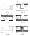
- Figure 2a to 2f illustrate a method of fabricating the device according to the present invention.
- Figure 3 shows a radar device according to the present invention.
- Preferred embodiments of the present invention which are millimetre wave antenna micromachined on an MCM-D silicon platform are described hereunder. It is designed for radiating above 20 GHz.
- the radiating aperture of this antenna is a micromachined waveguide.
- the aperture is etched in the bulk of the silicon substrate.
- the cross section of the micromachined waveguide can take a rectangular (Figs. 1a and 1b) or a circular (Figs. 1c and 1d) cross section or a cross section of any geometry.
- the cavity may be filled with a low loss dielectric, material such as a polymer material (BCB), to shrink the antenna dimensions.
- BCB polymer material
- the proposed antenna's are fed by a coplanar waveguide (CPW) realised on the side of the substrate of the antenna facing the MCM-D substrate but separated therefrom by a dielectric material.
- CPW coplanar waveguide
- the electromagnetic coupling from the feeding CPW to the antenna is achieved through a slot etched in the metal base of the aperture waveguide.
- the coupling slot has the same shape as the waveguide cross section.
- Figs. 1a and 1b show a rectangular opening (slot) (37a) in the base of a micromachined rectangular waveguide (33a) while Figs. 1c et 1b show a circular opening (slot) (37b) in the base of a micromachined circular waveguide (33b).
- the feeding CPW (23) are also shown on these Figures.
- Several radiating ends of the feeding CPW are used, such as open, short, capacitive, and inductive ends.
- the frequency of the signal radiated by the antenna is the frequency of the signal propagating in the CPW waveguide, and fed to the antenna by electromagnetic coupling through the slot.
- the radiated wavelength is basically not set by the waveguide dimensions.
- the waveguide dimensions actually define the cut-off frequency of the respective modes which could be excited by a fed signal of given frequency.
- a cylindrical aperture antenna is described on Fig. 1c.
- the walls of the cylinder are sputter coated with TiW/Au.
- An opening is made in this metal in the bottom of the cylinder, in order to feed (excite) the antenna located on chip's backside through a microstrip tine leaving the oscillator, and located on the frontside of the substrate.
- the hole is either
- a rectangular aperture antenna can be manufactured similarly.
- the process of fabrication of an antenna according to the present invention starts with a double side polished low resistivity silicon wafer (antenna substrate) (31), wherein the following steps are performed:
Landscapes
- Engineering & Computer Science (AREA)
- Manufacturing & Machinery (AREA)
- Variable-Direction Aerials And Aerial Arrays (AREA)
- Waveguide Aerials (AREA)
- Radar Systems Or Details Thereof (AREA)
Abstract
Description
- The present invention relates to a millimetre wave antenna, a device integrating such antenna and a method for manufacturing same.
- Microwave antennas are usually to emit radiation in a medium such as air, ..., with a sufficient precision of directivity and are to be sufficiently small. State of the art millimetre wave antennas are, thanks to the antennas scaling laws, inherently small enough for being arrangeable in highly directive arrays. The larger the number of radiating elements in the array, the more directive the antenna can be. If the directivity of one element is already high, the number of elements required for reaching a target directivity will be smaller, and therefore the antenna itself can be smaller.
- The state of the art directive antennas in the millimetre wave range are planar antennas, with patch antennas being the most widely used.
- These planar antennas are very attractive for use within compact communication systems, (telecommunication, WLAN) owing to their simple integration with driving electronics and microwave circuits. However, they suffer from two serious disadvantages which are the limited bandwidth and the substrate losses.
- Millimetre wave antennas furthermore find applications within the automotive market as a FLAR (Forward Looking Automobile Radar) or as automobile sensors.
- Thus the millimetre wave portion of the spectrum is used for at least two important applications requiring small and directive antennas:
- Wireless data transmission (38 GHz).
- Automobile anticollision radar's (77 GHz).
- Automotive applications are considered one of the two most important applications [H.H. Meinel, "Commercial Applications of Millimetre Waves. History, Present Status, and Future Trends", IEEE Transactions on Microwave Theory and Techniques. Vol.43. Nr 7, July 1995, pp 1639-1653.] in the millimetre wave communication range, the second being the short haul transmission links for PCN installations.
- A FLAR is a radar used for measuring the relative velocity between two vehicles in a lane, and the distance between these vehicles, in order to issue warnings to the vehicle drivers. The FLAR consists of different parts:
- A set of antennas (Tx and Rx) for emitting a millimetre wave signal, and receiving the corresponding signal echoed by any obstacle on the lane, both signals propagating in the air.
- MMICs (Monolithic Microwave Integrated Circuit) called "transceiver", which comprises mixers, low noise amplifiers, power amplifiers, and an oscillator. The transceiver insures the generation of a millimetre wave oscillation, the mixing thereof with a signal of lower frequency (IF), and the amplification before emission. The transceiver also insures the recovery of the millimetre wave echoed signal and its downconverting to IF frequency range.
- Analogue and digital processing units.
- The FLARs are to be designed for operation at different frequencies, depending on the geographic area:
- in Europe, at 76,5 GHz
- in Japan, at 60 GHz
- in the United States, there are several frequency bands allocated by the US Federal Communications Commission (F.C.C) for traffic radar's, including the 10.5 GHz and 24.1 GHz frequencies and the 33.4 to 36 GHz range. Radar's operating at 94 GHz are also under development.
- Radar systems for the automobile have been studied for more than 20 years by major car companies in collaboration with RF companies and chips manufacturers.
- Basically, there are two dominating factors that drive the technology for millimetre wave automotive radar's: cost and hardware size. Low cost is the key factor for consumers to accept the radar as a safety and affordable component in their vehicle. The size constraint is essential for easy integration of the radar on the vehicle without major impact on the vehicle design and performance.
- An antenna for an Automobile anticollision radar (77 GHz) system needs to fulfil the requirements of scanning the road ahead. Thus, radar techniques are used requiring antennas which are:
- Directive: there should be no confusion between in line and adjacent lanes.
- Compact: The antenna size should not be detrimental to the car aesthetics. Furthermore, an easy and straightforward link between stearing electronics and the antenna should be feasible.
- Most of the radar developments so far are built around GaAs (or other III-V) MMIC's, but also other developments have been going on. Daimler Benz is active in developing SIMMWIC and has reported mid 1995 the successful fabrication of
- schottky diodes for mixers
- PJN diodes for switches
- low noise oscillators using SiGe HBT's
- IMPATT diodes for mmwave power generation on high resistivity Si (> 10k.cm). [J F. Luy et al, "Si/SiGe MMIC's". IEEE Transactions on Microwave Theory and Techniques. Vol.43. N04, April 1995, pp 706-719 and A. Stiller et al, A Monolithic Integrated Millimetre Wave Transmitter for Automotive Applications. IEEE Transactions on Microwave Theory and Techniques. Vol.43. Nr 7, July 1995, pp 1654-1657.]
- Another approach followed by Hughes Research Labs is the flip-chip mounting of GaAs MMIC chips on low cost duroid substrates. Successful realisation of a mixer for the 77 GHz by flip-chip mounting GaAs schottky diodes was reported [R.S. Virk et al, "A Low Cost W-Band MIC Mixer Using Flip-Chip Technology", IEEE Microwave and Guided Wave Letters. Vol. 7, Nr 9, September 1997, pp 294-296.]
- Therefore, the cost of devices fabricated in a III-V process technology remains higher than silicon-based devices.
- Furthermore, it is known that the radar size can be reduced by the following measures
- By higher degrees of integration i.e. regrouping the different functional blocks of the communication system. This is not straightforward in practise: trade-offs are imposed on the performance of the different elements brought together;
- By stacking several chips; ([M. Stotz et al, "Planar Millimetre Wave Antennas Using SiNx Membranes on GaAs", IEEE Transactions on Microwave Theory and Techniques, Vol.44. Nr 9, September 1996. Pp 1593-1595.].
- By suitable antenna design. The radar size however cannot be reduced to less than the area occupied by the antenna. In practise, the antenna size is fixed by the radar specification of directivity.
- Thus, there is a need for the development of a millimetre wave communication device that includes an antenna
- which can be fabricated at low cost but at the same time with sufficient precision;
- which has a sufficient directivity;
- that is compact and can be integrated with other electronic components of the device;
- that has a sufficiently large band width and is sufficiently efficient.
- Several documents, among them W096/27913, US-5,724,049 and EP-0939451 (not yet published at the date of the priority of the present application), are describing microstrip-to-waveguide antenna's. The main problem of using such technology is that the thickness of the dielectric and conductive layer is rather important. Another drawback of this microstrip technology is that an additional impedance matching between the slot and the external space is required. For instance, in documents US-5,724,049 and EP-0939451, it is described that a dedicated dielectric layer is added in order to obtain the desired impedance, which will avoid undesired reflection of signals. Furthermore, the directivity of said devices will not be high enough to be used in several applications, and more particularly for automobile anti-collision radars.
- A first aim of the present invention is to provide a suitable antenna for millimetre wave communication device applications. The antennas according to the present invention are millimetre wave antennas emitting radiation, having high directivity and high efficiency. The antennas can be used for instance for telecommunications and for automotive radars.
- Another aim is that the antenna can be integrated with other parts of a device for communication applications. Specifically the applications of wireless data communication and automotive radar devices are aimed for. It is an aspect of such application that a reasonably compact antenna is needed. The compactness of the antenna allows for a dense integration with other components enhancing its use in automotive applications requiring portable devices.
- Yet, another aim is to provide millimetre wave antennas that are
- of comparable or same size as "patch antennas",
- at least as directive as the "patch antenna",
- if possible made on a similar technological platforms,
- having as additional features a larger bandwidth, and
- being more efficient (with less or no substrate losses) than patch antennas.
- The present invention relates to a device for emitting and/or receiving a signal in the millimetre wave range in a medium, characterised in that said device comprises a MCM substrate on which there are at least a first metallic layer, a first insulating layer and a second substrate, said second substrate comprising a cavity extending to said first insulating layer, and having a second metallic layer at least covering the walls of said cavity and covering part of said first insulating layer in order to have an opening in said second metallic layer.
- Said medium can be air, vacuum and more generally a non solid medium capable of transmitting electromagnetic radiation.
- In said second metallic layer, there is a discontinuity in order to create the feeding waveguide.
- Said feeding waveguide can also be a thin strip having its end not facing said opening or it can be a tip created in the metallic layer.
- The structure of the first metallic layer, the first insulating layer and the second substrate comprising a cavity extending to said first insulating layer, and having a second metallic layer at least covering the walls of said cavity and covering part of said first insulating layer in order to form an opening in said second metallic layer, can form an antenna on its own.
- By realising said antenna on a MCM substrate by micromachining process, there is no need to provide an additional impedance matching between the opening (slot) and the external space (medium).
- The second substrate of the antenna itself can be made of any material that allows for manufacturing with a reasonable precision and adequate dimensions. Examples of such substrates are semiconductor materials such as silicon wafers: silicon allows for the use of established micromachining techniques in order to fabricate the proper device structure.
- The second substrate of the antenna itself can also consist of III-V semiconductors, a ceramic (Al2O3, AlN), a glass, a plastic, a polymer material or any combination thereof or such materials in a matrix of another material or vice-versa. Fabrication techniques of the proper device structure can include laser cutting, ultrasonic dilling, injection moulding or similar techniques known in the art.
- The second substrate of the antenna itself can also be a metallic substrate, in which case the second metallic layer is the outer layer of said substrate. Another substrate having a dielectric insulating layer and the first metallic layer can then be attached by any means known in the art to the metallic substrate with a membrane therebetween, in order to achieve the device structure of the invention. This fabrication technique of working with two separated substrates that are connected can also be applied to any other of the above-referenced substrates.
- Another way to produce the device of the invention with a specific geometry is using a moulding process for the antenna itself. The production is then done by injection moulding or any other way of making replicates. The mould can then be made with LIGA using X-ray or photolithography, for instance deep UV lithography, which allows to achieve very small dimensions. Plastics such as PMMA, PEEK, PVE and PEI can be used as a substrate. The use of plastics for making microstructures in plastic is known in the art.
- The mould fabricated by means of the above-defined methods can be used again as a tool for further replication processes, e.g. as mould inserts for micromoulding or reaction injection moulding. Materials to be used for the replication processes are usually melted polymers and casting resins. After hardening in the metallic forms, the mould materials have reached a sufficient strength and the separation of mould and mould insert can take place. For the realisation of micromoulding and micro-reaction injection moulding the extremely low roughness of the walls of LIGA fabricated mould inserts is most important.
- Materials that have been used for microreplication include low viscosity thermoplastic polymers like polymethyl methacrylate (PMMA), polyoxymethylene (POM), polyamide (PA) or polycarbonate, as well as reaction resins based on methacrylates, silicones and caprolactames. However, many more materials could be used. Except for filled moulding materials, almost any material suitable for macroscopic moulding can be used for micromoulding.
- Ceramic microstructures can be fabricated by slurry casting, by using sol-gel processes or by means of electrophoretic and other processes. It is e.g. possible to fill the gaps of a LIGA fabricated polymer structure with a slurry of microcrystalline ceramic powder. After drying and firing, the polymer degrades, evaporates or is oxidised, which results in a ceramic microstructure. The characteristic dimensions of the ceramic structures are smaller than the polymer form, due to shrinkage during the firing process. Mechanically very stable and temperature persistent materials can thus be microstructured by means of the LIGA process.
- In a preferred embodiment of the present invention, the second substrate of the antenna itself can essentially consist of Si having the first insulating layer consisting essentially in Si-oxide material.
- The antenna device can also comprise a further polymer layer between the first metallic layer and the second substrate or said first insulating layer can be itself a further polymer layer. The polymer layer for instance can be a dielectric such as PCB or PBO (polybenzoxyzazole). In fact, for a number of applications, the first insulating layer is to have high-quality dielectric properties. The applications requesting such properties are those wherein a transmission line is made in the first metallic layer. With the high-quality dielectric material, substrate losses during signal transmission in the transmission line are avoided.
- The second substrate of the antenna itself can also be an MCM-D substrate. Suitable materials for the first metallic layer can include low-resistive metals such as Cu, Ag, Al, Au and alloys thereof.
- The cavity is preferably filled with a low-loss polymer material, preferably a dielectric comprising BCB, to increase the electrical length of the cavity. Yet another material can be PBO.
- The device can further comprise means for generating an electrical signal in the first metallic layer. The high-quality dielectric properties can also be important in order to achieve a good coupling between the feeding network of the device generating a signal in the first metallic layer and the antenna of the invention, without major losses in the first insulating layer. The coupling to be achieved depends on the frequency aimed for in a particular application.
- The waveguide is excited by a feed line of coplanar type located on the wafer front side. The feed line is in a metal layer separated by a dielectric layer from the substrate.
- Excitation is done by coupling the cavity to the feed line through a feed slot in the bottom of the metallised cavity.
- Another device for emitting and/or receiving a signal in the millimetre wave range according to the present invention is characterised in that it comprises an array of any of the precited devices.
- Another device for emitting and/or receiving a signal in the millimetre wave range according to the present invention is configured as a flipchip of any of the precited devices and a CMOS substrate with integrated circuits having a functionality therein, possibly both being integrated on said MCM substrate.
- In the method of operating the device of the invention, the signal is generated in the first metallic layer, said signal being transmitted to said second metallic layer and being emitted in the form of radiation therefrom.
- The present invention furthermore relates to a method for manufacturing an antenna for emitting and/or receiving a signal in the millimetre wave range, characterised in that it comprises the following steps:
- depositing a first insulating layer on a first side of a (second) substrate,
- depositing a first metallic layer on said first insulating layer,
- defining, for instance etching, a cavity with predetermined dimensions in said (second) substrate at a second side thereof,
- depositing a second metallic layer at said second side of said (second) substrate, and
- removing a part of said second metallic layer located at the bottom of said cavity in order to have an opening in said second metallic layer.
- Said antenna is created on a MCM wafer possibly having other circuits for system integration.
- The method can further comprise the steps of:
- depositing a second insulating layer on said second side of said substrate and
- creating an opening in said second insulating layer, the cavity being etched through said opening.
- This method can further comprise the step of filling said cavity with a polymer, preferably BCB, the substrate being an MCM-D wafer.
- In an embodiment of the method of the invention, the substrate can comprise Si and the first insulating layer can comprise a Si-oxide layer and a polymer layer, said polymer preferably comprising BCB.
- Figures 1a to 1d are representing two distinct embodiments of the cavity of the antenna according to the present invention are shown. Parameter values are given in Table 1 and Table 2.
- Figure 2a to 2f illustrate a method of fabricating the device according to the present invention.
- Figure 3 shows a radar device according to the present invention.
- The present invention is described in details based on a device having the following features:
- Advanced micromachining (deep dry etch), microelectronics (SiGe/Si HBTs) and assembly techniques (flip-chip) are combined with CMOS processing, to make a self packaged, low cost, small size transmitter/receiver device. The high precision of Silicon manufacturing techniques allows for making a device with high precision.
- The transmitter/receiver antenna can be designed for minimised size and maximal directivity.
- The device can be used in the automotive market (FLAR), but it can easily be adapted for other automobile sensors (Doppler radar) and to other areas of applications (namely millimetre wave communications, such as in WLANs).
- It is a MCM-D wafer, on which several circuits for system integration with the antenna are assembled.
- In this embodiment of the present invention, it is preferred:
- To use highly resistive Si as the substrate of the antenna. The RF functions can be integrated in the Si substrate or can be defined in other components, for instance in CMOS technology, CMOS-SiGe, bipolar technology or III-V technology, that are mounted on the first metallic layer. This mounting step can be achieved for instance by flip-chip mounting, ball-grid array technology and other techniques known in the art. It is nowadays practical to define the high frequency (>5 GHz) RF function in another substrate material than Si.
- To adopt a directive antenna element design for the antenna, and to machine this element (alone, or arranged in arrays) into the bulk of the resistive silicon backside.
- Because the active element chips in a millimetre wave transceiver device are made in a variety of technologies, an attractive direction for its fabrication is the bonding of these multiple chips on one platform, which might support passives as well. Such a platform is available in the multilayer thin film technology as used in the MCM-D, technology which is well known in the art.
- Preferred embodiments of the present invention which are millimetre wave antenna micromachined on an MCM-D silicon platform are described hereunder. It is designed for radiating above 20 GHz. The radiating aperture of this antenna is a micromachined waveguide. The aperture is etched in the bulk of the silicon substrate. The cross section of the micromachined waveguide can take a rectangular (Figs. 1a and 1b) or a circular (Figs. 1c and 1d) cross section or a cross section of any geometry. The cavity may be filled with a low loss dielectric, material such as a polymer material (BCB), to shrink the antenna dimensions.
- The proposed antenna's are fed by a coplanar waveguide (CPW) realised on the side of the substrate of the antenna facing the MCM-D substrate but separated therefrom by a dielectric material. The electromagnetic coupling from the feeding CPW to the antenna is achieved through a slot etched in the metal base of the aperture waveguide. The coupling slot has the same shape as the waveguide cross section.
- Figs. 1a and 1b show a rectangular opening (slot) (37a) in the base of a micromachined rectangular waveguide (33a) while Figs. 1c et 1b show a circular opening (slot) (37b) in the base of a micromachined circular waveguide (33b).
- The feeding CPW (23) are also shown on these Figures. Several radiating ends of the feeding CPW are used, such as open, short, capacitive, and inductive ends.
- The frequency of the signal radiated by the antenna is the frequency of the signal propagating in the CPW waveguide, and fed to the antenna by electromagnetic coupling through the slot. In other words, the radiated wavelength is basically not set by the waveguide dimensions. The waveguide dimensions actually define the cut-off frequency of the respective modes which could be excited by a fed signal of given frequency.
- A cylindrical aperture antenna is described on Fig. 1c. The walls of the cylinder are sputter coated with TiW/Au. An opening is made in this metal in the bottom of the cylinder, in order to feed (excite) the antenna located on chip's backside through a microstrip tine leaving the oscillator, and located on the frontside of the substrate.
- In order to cancel the high order resonating modes of the antenna, the hole is either
- filled with a low loss dielectric
- or half wavelength deep.
- In order to make the antenna a resonator, the following is done:
- The cylinder is etched in Si, using a deep dry etch recipe from STS.
- A photolithographic resist layer Shiplev PEPR 2400 [S. Linder et al. "Photolithography in anisotropically etched grooves", Proc. IEEE MEMS Worskhop San Diego. CA, pp 38-43.] based on combined planar and non planar technology (the term "non planar technology" refers in this case to the metallic waveguide) will be electroplated on MMIC chip's backside. An opening in resist is performed, and the slot etched (the front side being resist protected).
- BCB can be dispensed in the cavity (or if not possible, the depth of this cavity will equal half wavelength).
- A rectangular aperture antenna can be manufactured similarly.
- The directivity of the integrated antenna was evaluated analytically. An empty waveguide was assumed for these first calculations (no BCB filling).
- From results summarised in Tables 1 and 2 it can be shown that:
- the circular aperture antenna compares in size with the micropatch, but is more directive (7.4dB against 5.4dB for the micropatch) and obviously more robust. The BCB filling is expected to further improve the directivity of the circular aperture antenna.
- the rectangular aperture antenna is even more directive (9.8 dB against 5.4 dB for the micropatch), it is observed however that the rectangular aperture antenna features a larger size than the circular one (there is room in a rectangular aperture for two rectangular micropatch. And a two elements array factor should therefore be considered).
- As represented in Figs. 2, the process of fabrication of an antenna according to the present invention starts with a double side polished low resistivity silicon wafer (antenna substrate) (31), wherein the following steps are performed:
- For DRIE dry etching through the silicon wafer (31), a thick oxide layer (21) is CVD deposited on the wafer backside, and further patterned into an oxide hard mask (see Fig. 3a).
- The MCM-D circuit (100) can be made on the front side of a silicon wafer using either spin-on dielectric (thick BCB or polyimide), and metal deposition/patterning as described in J F. Luy et al, "Si/SiGe MMIC's". IEEE Transactions on Microwave Theory and Techniques. Vol.43. N04, April 1995, pp 706-719.
- The hard mask is aligned with the MCM-D patterns on the wafer front side, in order to align the tip (23) of the coupling CPW (25), the etched slot (29), and the waveguide. Double side alignment is performed on an Electronic Vision dedicated equipment (see Fig. 2b).
- At this point, a resist protective layer (not represented) is coated on the MCM-D circuit (100).
- A cavity (27) with desired cross section is etched vertically through the bulk of the silicon wafer (see Fig. 2c), using an STS recipe applied on wafer backside. The etch stops as soon as the interface between the silicon and the dielectric layer is reached, thanks to etch selectivity.
- The residual masking oxide is removed using dry etching. The backside is then metallised with a blanket layer (33) of sputtered metal (see Fig. 2d).
- Copper is then sputtered on the wafer backside. Copper is used as a seed layer for coating electrodeposable resist (33) of type PEPR 2400 by Shipley.
- Next, resist is exposed through a photolithographic mask, then developed. The unprotected copper is etched away. This completes the opening of the feed slot in the bottom of the metallised cavity (27). Resist is then stripped.
- A layer of electrophoretic PEPR 2400 photolithographic resist (37) from Shipley is electroplated and baked. The resist is further exposed (see Fig. 2d), and developed, this leaves an opening (37) in the resist in the bottom of the metallised cavity (27). The exposed metal is wet etched (see Fig. 2e).
- The PEPR 2400 resist and the protective layer are stripped in a compatible solvent (e.g., acetone or hot resist stripper).
- Finally (optional), BCB (41) can be dispensed in the cavity (27) (see Fig. 2f).
- One can envisage to process two silicon chips separately, one highly resistive supporting all the RF functions plus the antenna (as e.g. in example 1) , the second supporting all the CMOS and IF functions. These can to flipchip assemble the 2 chips, connecting the RF and IF circuits where necessary on a MCM-D substrate.
- The result will be a low cost fully integrated, compact self packaged and robust radar as shown on Fig. 3.


Claims (17)
- Device for emitting and/or receiving a signal in the millimetre wave range, characterised in that said device comprises a MCM substrate (100) on which there are at least a first metallic layer (25), a first insulating layer (21), a second substrate (31), said second substrate comprising a cavity (27) extending up to said first insulating layer (21), and having a second metallic layer (33) at least covering the walls of said cavity (27) and covering part of said first insulating layer (21) in order to have an opening (37) in said second metallic layer (33) .
- Device as in claim 1, wherein said first metallic layer has a discontinuity (23) facing or not said opening (37) of said cavity (27).
- Device as in claim 1 or 2, wherein said second substrate is selected from the group consisting of semiconductors, plastic, polymers or ceramic materials.
- Device as in any of the preceding claims, characterised in that said second substrate essentially consists of Si and the first insulating layer comprises a Si oxide layer.
- Device as in any of the preceding claims, characterised in that the second substrate is an MCM-D substrate.
- Device as in any of the preceding claims, characterised in that said first insulating layer (21) is made of a polymer material, preferably a dielectric comprising BCB, PCB or PBO.
- Device as in any of the preceding claims, characterised in that the cavity (27) is filled with a polymer material (41), preferably a dielectric comprising BCB, PCB or PBO.
- Device as in any of the preceding claims, characterised in that the device further comprises means for generating an electrical signal in the first metallic layer (25).
- Device for emitting and/or receiving a signal in the millimetre wave range, characterised in that it comprises an array of devices as in any of the claims 1 to 8.
- Device for emitting and/or receiving a signal in the millimetre wave range, characterised in that it comprises a flipchip of a device as in any of the claims 1 to 8 and a CMOS substrate, possibly both being integrated on a MCM substrate.
- Method for manufacturing a device for emitting and/or receiving a signal in the millimetre wave range, characterised in that it comprises the following steps:depositing a first insulating layer (21) on a first side of a substrate (31),depositing a first metallic layer (25) on said first insulating layer (21),defining a cavity (27) with predetermined dimensions in said substrate (31) at a second side thereof,depositing a second metallic layer (33) at said second side of said substrate (31), andremoving a part of said second metallic layer located at the bottom of said cavity in order to create an opening (37) in said metallic layer (33).
- The method as in claim 11, further comprising the steps of depositing a second insulating layer on said second side of said substrate and creating an opening in said second insulating layer, the cavity being etched through said opening.
- The method as in claim 11 or 12, further comprising the step of filling said cavity with a polymer material (41), preferably a dielectric comprising BCB.
- The method as in any of the claims 11 to 13, characterised in that the substrate is an MCM-D substrate.
- The method as in any of the preceding claims 11 to 14, characterised in that the substrate comprises Si and the first insulating layer comprises a Si oxide layer and a polymer layer, said polymer preferably comprising BCB.
- The method as any of the claims 11 to 15, wherein said substrate is realised on a MCM integrating wafer.
- A method of operating the device of claim 1, characterised in that a signal is generated in the first metallic layer, said signal being transmitted to said second metallic layer and being emitted in the form of radiation therefrom.
Priority Applications (1)
| Application Number | Priority Date | Filing Date | Title |
|---|---|---|---|
| EP20000870097 EP1052726B1 (en) | 1999-05-05 | 2000-05-05 | Manufacturing method for a slot coupled micromachined waveguide antenna |
Applications Claiming Priority (5)
| Application Number | Priority Date | Filing Date | Title |
|---|---|---|---|
| EP99870096 | 1999-05-05 | ||
| EP99870096 | 1999-05-05 | ||
| EP99870129A EP1063723A1 (en) | 1999-06-22 | 1999-06-22 | Slot coupled micromachined waveguide antenna |
| EP99870129 | 1999-06-22 | ||
| EP20000870097 EP1052726B1 (en) | 1999-05-05 | 2000-05-05 | Manufacturing method for a slot coupled micromachined waveguide antenna |
Publications (2)
| Publication Number | Publication Date |
|---|---|
| EP1052726A1 true EP1052726A1 (en) | 2000-11-15 |
| EP1052726B1 EP1052726B1 (en) | 2008-02-20 |
Family
ID=27223753
Family Applications (1)
| Application Number | Title | Priority Date | Filing Date |
|---|---|---|---|
| EP20000870097 Expired - Lifetime EP1052726B1 (en) | 1999-05-05 | 2000-05-05 | Manufacturing method for a slot coupled micromachined waveguide antenna |
Country Status (1)
| Country | Link |
|---|---|
| EP (1) | EP1052726B1 (en) |
Cited By (3)
| Publication number | Priority date | Publication date | Assignee | Title |
|---|---|---|---|---|
| EP1784063A1 (en) * | 2005-11-08 | 2007-05-09 | Alcatel Lucent | Circuit board with microelectronic elements assembled thereon and method for producing such circuit board |
| US9270005B2 (en) | 2011-02-21 | 2016-02-23 | Siklu Communication ltd. | Laminate structures having a hole surrounding a probe for propagating millimeter waves |
| US9496593B2 (en) | 2011-02-21 | 2016-11-15 | Siklu Communication ltd. | Enhancing operation of laminate waveguide structures using an electrically conductive fence |
Families Citing this family (1)
| Publication number | Priority date | Publication date | Assignee | Title |
|---|---|---|---|---|
| CN110401022B (en) * | 2019-08-02 | 2021-01-22 | 电子科技大学 | Millimeter-wave high-gain slot array antenna based on MEMS technology |
Citations (6)
| Publication number | Priority date | Publication date | Assignee | Title |
|---|---|---|---|---|
| DE4208058A1 (en) * | 1992-03-13 | 1993-09-16 | Deutsche Aerospace | Waveguide to microstrip transition for micro and millimetre range - has planar substrate with microstrip line and coupling slot to waveguide formed on separate planar layer. |
| US5414394A (en) * | 1992-12-29 | 1995-05-09 | U.S. Philips Corporation | Microwave frequency device comprising at least a transition between a transmission line integrated on a substrate and a waveguide |
| WO1996027913A1 (en) * | 1995-03-06 | 1996-09-12 | Valtion Teknillinen Tutkimuskeskus | Microstrip-to-waveguide transition |
| US5724049A (en) * | 1994-05-23 | 1998-03-03 | Hughes Electronics | End launched microstrip or stripline to waveguide transition with cavity backed slot fed by offset microstrip line usable in a missile |
| WO1998047198A2 (en) * | 1997-03-25 | 1998-10-22 | The University Of Virginia Patent Foundation | A preferential crystal etching technique for the fabrication of millimeter and submillimeter wavelength horn antennas |
| EP0939451A1 (en) * | 1998-02-27 | 1999-09-01 | Kyocera Corporation | Slot antenna |
-
2000
- 2000-05-05 EP EP20000870097 patent/EP1052726B1/en not_active Expired - Lifetime
Patent Citations (6)
| Publication number | Priority date | Publication date | Assignee | Title |
|---|---|---|---|---|
| DE4208058A1 (en) * | 1992-03-13 | 1993-09-16 | Deutsche Aerospace | Waveguide to microstrip transition for micro and millimetre range - has planar substrate with microstrip line and coupling slot to waveguide formed on separate planar layer. |
| US5414394A (en) * | 1992-12-29 | 1995-05-09 | U.S. Philips Corporation | Microwave frequency device comprising at least a transition between a transmission line integrated on a substrate and a waveguide |
| US5724049A (en) * | 1994-05-23 | 1998-03-03 | Hughes Electronics | End launched microstrip or stripline to waveguide transition with cavity backed slot fed by offset microstrip line usable in a missile |
| WO1996027913A1 (en) * | 1995-03-06 | 1996-09-12 | Valtion Teknillinen Tutkimuskeskus | Microstrip-to-waveguide transition |
| WO1998047198A2 (en) * | 1997-03-25 | 1998-10-22 | The University Of Virginia Patent Foundation | A preferential crystal etching technique for the fabrication of millimeter and submillimeter wavelength horn antennas |
| EP0939451A1 (en) * | 1998-02-27 | 1999-09-01 | Kyocera Corporation | Slot antenna |
Non-Patent Citations (2)
| Title |
|---|
| LUBECKE V M ET AL: "MICROMACHINING FOR TERAHERTZ APPLICATIONS", IEEE TRANSACTIONS ON MICROWAVE THEORY AND TECHNIQUES,US,IEEE INC. NEW YORK, vol. 46, no. 11, PART 02, pages 1821-1831, XP000785371, ISSN: 0018-9480 * |
| VANDENBERG N L ET AL: "A BANDWIDTH ENHANCEMENT TECHNIQUE FOR MICROSTRIP FED SLOT ARRAYS", PROCEEDINGS OF THE ANTENNAS AND PROPAGATION SOCIETY ANNUAL MEETING,US,NEW YORK, IEEE, vol. -, pages 1824-1827, XP000239314, ISBN: 0-7803-0144-7 * |
Cited By (3)
| Publication number | Priority date | Publication date | Assignee | Title |
|---|---|---|---|---|
| EP1784063A1 (en) * | 2005-11-08 | 2007-05-09 | Alcatel Lucent | Circuit board with microelectronic elements assembled thereon and method for producing such circuit board |
| US9270005B2 (en) | 2011-02-21 | 2016-02-23 | Siklu Communication ltd. | Laminate structures having a hole surrounding a probe for propagating millimeter waves |
| US9496593B2 (en) | 2011-02-21 | 2016-11-15 | Siklu Communication ltd. | Enhancing operation of laminate waveguide structures using an electrically conductive fence |
Also Published As
| Publication number | Publication date |
|---|---|
| EP1052726B1 (en) | 2008-02-20 |
Similar Documents
| Publication | Publication Date | Title |
|---|---|---|
| EP1398848B1 (en) | Laminated aperture antenna and multi-layered wiring board comprising the same | |
| US6191740B1 (en) | Slot fed multi-band antenna | |
| US6815739B2 (en) | Radio frequency microelectromechanical systems (MEMS) devices on low-temperature co-fired ceramic (LTCC) substrates | |
| CN101743665B (en) | Improvements in Reconfigurable Antennas and Improvements Related thereto | |
| US5982250A (en) | Millimeter-wave LTCC package | |
| KR100552658B1 (en) | Resonant cavity for phase noise reduction of voltage controlled oscillator | |
| WO2009023551A1 (en) | Hybrid integrated mems reconfigurable antenna array (himra) | |
| JP2013521508A (en) | Radar system and manufacturing method thereof | |
| US7545339B2 (en) | Planar antenna apparatus for ultra wide band applications | |
| EP1052726B1 (en) | Manufacturing method for a slot coupled micromachined waveguide antenna | |
| Pfahler et al. | Towards 3D-Printed Antenna in Package Solutions for THz-Applications | |
| JP2001156536A (en) | Slot array antenna, waveguide manufacturing method and circuit forming method | |
| Svedin et al. | A micromachined 94 GHz dielectric resonator antenna for focal plane array applications | |
| EP1063723A1 (en) | Slot coupled micromachined waveguide antenna | |
| WO1998047198A2 (en) | A preferential crystal etching technique for the fabrication of millimeter and submillimeter wavelength horn antennas | |
| EP1041667A2 (en) | Cavity resonator for reducing phase noise of voltage controlled oscillator and method for fabricating the same | |
| JPH10261917A (en) | Millimeter wave transceiver | |
| US20250015506A1 (en) | Metamaterial-based compact antenna-in-package solutions in frequency handover applications | |
| JP2005204344A (en) | Slot array antenna, waveguide manufacturing method and circuit forming method | |
| Wang et al. | 79-GHz LTCC RF-frontend deploying 45 degree linear-polarized vertical parallel-feed antennas | |
| Ellis et al. | A wideband CPW-fed microstrip antenna at millimeter-wave frequencies | |
| Sabban | 7 Wideband RF | |
| Koga et al. | Cavity-backed MEMS patch antennas on double-layer silicon wafers | |
| JP2002084110A (en) | Power combiner / distributor | |
| TAKAHASHI et al. | A compact V-band filter/antenna integrated receiver IC built on Si-micromachined BCB suspended structure |
Legal Events
| Date | Code | Title | Description |
|---|---|---|---|
| PUAI | Public reference made under article 153(3) epc to a published international application that has entered the european phase |
Free format text: ORIGINAL CODE: 0009012 |
|
| AK | Designated contracting states |
Kind code of ref document: A1 Designated state(s): AT BE CH CY DE DK ES FI FR GB GR IE IT LI LU MC NL PT SE |
|
| AX | Request for extension of the european patent |
Free format text: AL;LT;LV;MK;RO;SI |
|
| 17P | Request for examination filed |
Effective date: 20001218 |
|
| AKX | Designation fees paid |
Free format text: AT BE CH CY DE DK ES FI FR GB GR IE IT LI LU MC NL PT SE |
|
| 17Q | First examination report despatched |
Effective date: 20050330 |
|
| 17Q | First examination report despatched |
Effective date: 20050330 |
|
| RTI1 | Title (correction) |
Free format text: MANUFACTURING METHOD FOR A SLOT COUPLED MICROMACHINED WAVEGUIDE ANTENNA |
|
| GRAP | Despatch of communication of intention to grant a patent |
Free format text: ORIGINAL CODE: EPIDOSNIGR1 |
|
| GRAS | Grant fee paid |
Free format text: ORIGINAL CODE: EPIDOSNIGR3 |
|
| GRAA | (expected) grant |
Free format text: ORIGINAL CODE: 0009210 |
|
| AK | Designated contracting states |
Kind code of ref document: B1 Designated state(s): AT BE CH CY DE DK ES FI FR GB GR IE IT LI LU MC NL PT SE |
|
| REG | Reference to a national code |
Ref country code: GB Ref legal event code: FG4D |
|
| REG | Reference to a national code |
Ref country code: CH Ref legal event code: EP |
|
| RAP2 | Party data changed (patent owner data changed or rights of a patent transferred) |
Owner name: KU LEUVEN RESEARCH & DEVELOPMENT Owner name: INTERUNIVERSITAIR MICRO-ELEKTRONICA CENTRUM VZW |
|
| REG | Reference to a national code |
Ref country code: IE Ref legal event code: FG4D |
|
| REF | Corresponds to: |
Ref document number: 60038073 Country of ref document: DE Date of ref document: 20080403 Kind code of ref document: P |
|
| NLT2 | Nl: modifications (of names), taken from the european patent patent bulletin |
Owner name: INTERUNIVERSITAIR MICRO-ELEKTRONICA CENTRUM VZW EN Effective date: 20080319 |
|
| PG25 | Lapsed in a contracting state [announced via postgrant information from national office to epo] |
Ref country code: ES Free format text: LAPSE BECAUSE OF FAILURE TO SUBMIT A TRANSLATION OF THE DESCRIPTION OR TO PAY THE FEE WITHIN THE PRESCRIBED TIME-LIMIT Effective date: 20080531 Ref country code: FI Free format text: LAPSE BECAUSE OF FAILURE TO SUBMIT A TRANSLATION OF THE DESCRIPTION OR TO PAY THE FEE WITHIN THE PRESCRIBED TIME-LIMIT Effective date: 20080220 |
|
| NLV1 | Nl: lapsed or annulled due to failure to fulfill the requirements of art. 29p and 29m of the patents act | ||
| PG25 | Lapsed in a contracting state [announced via postgrant information from national office to epo] |
Ref country code: AT Free format text: LAPSE BECAUSE OF FAILURE TO SUBMIT A TRANSLATION OF THE DESCRIPTION OR TO PAY THE FEE WITHIN THE PRESCRIBED TIME-LIMIT Effective date: 20080220 |
|
| ET | Fr: translation filed | ||
| PG25 | Lapsed in a contracting state [announced via postgrant information from national office to epo] |
Ref country code: BE Free format text: LAPSE BECAUSE OF FAILURE TO SUBMIT A TRANSLATION OF THE DESCRIPTION OR TO PAY THE FEE WITHIN THE PRESCRIBED TIME-LIMIT Effective date: 20080220 |
|
| PG25 | Lapsed in a contracting state [announced via postgrant information from national office to epo] |
Ref country code: SE Free format text: LAPSE BECAUSE OF FAILURE TO SUBMIT A TRANSLATION OF THE DESCRIPTION OR TO PAY THE FEE WITHIN THE PRESCRIBED TIME-LIMIT Effective date: 20080520 Ref country code: PT Free format text: LAPSE BECAUSE OF FAILURE TO SUBMIT A TRANSLATION OF THE DESCRIPTION OR TO PAY THE FEE WITHIN THE PRESCRIBED TIME-LIMIT Effective date: 20080721 Ref country code: NL Free format text: LAPSE BECAUSE OF FAILURE TO SUBMIT A TRANSLATION OF THE DESCRIPTION OR TO PAY THE FEE WITHIN THE PRESCRIBED TIME-LIMIT Effective date: 20080220 Ref country code: DK Free format text: LAPSE BECAUSE OF FAILURE TO SUBMIT A TRANSLATION OF THE DESCRIPTION OR TO PAY THE FEE WITHIN THE PRESCRIBED TIME-LIMIT Effective date: 20080220 |
|
| PLBE | No opposition filed within time limit |
Free format text: ORIGINAL CODE: 0009261 |
|
| STAA | Information on the status of an ep patent application or granted ep patent |
Free format text: STATUS: NO OPPOSITION FILED WITHIN TIME LIMIT |
|
| PG25 | Lapsed in a contracting state [announced via postgrant information from national office to epo] |
Ref country code: MC Free format text: LAPSE BECAUSE OF NON-PAYMENT OF DUE FEES Effective date: 20080531 |
|
| REG | Reference to a national code |
Ref country code: CH Ref legal event code: PL |
|
| 26N | No opposition filed |
Effective date: 20081121 |
|
| PG25 | Lapsed in a contracting state [announced via postgrant information from national office to epo] |
Ref country code: LI Free format text: LAPSE BECAUSE OF NON-PAYMENT OF DUE FEES Effective date: 20080531 Ref country code: CH Free format text: LAPSE BECAUSE OF NON-PAYMENT OF DUE FEES Effective date: 20080531 |
|
| PG25 | Lapsed in a contracting state [announced via postgrant information from national office to epo] |
Ref country code: IE Free format text: LAPSE BECAUSE OF NON-PAYMENT OF DUE FEES Effective date: 20080505 |
|
| PG25 | Lapsed in a contracting state [announced via postgrant information from national office to epo] |
Ref country code: CY Free format text: LAPSE BECAUSE OF FAILURE TO SUBMIT A TRANSLATION OF THE DESCRIPTION OR TO PAY THE FEE WITHIN THE PRESCRIBED TIME-LIMIT Effective date: 20080220 |
|
| PG25 | Lapsed in a contracting state [announced via postgrant information from national office to epo] |
Ref country code: IT Free format text: LAPSE BECAUSE OF FAILURE TO SUBMIT A TRANSLATION OF THE DESCRIPTION OR TO PAY THE FEE WITHIN THE PRESCRIBED TIME-LIMIT Effective date: 20080220 |
|
| PG25 | Lapsed in a contracting state [announced via postgrant information from national office to epo] |
Ref country code: LU Free format text: LAPSE BECAUSE OF NON-PAYMENT OF DUE FEES Effective date: 20080505 |
|
| PG25 | Lapsed in a contracting state [announced via postgrant information from national office to epo] |
Ref country code: GR Free format text: LAPSE BECAUSE OF FAILURE TO SUBMIT A TRANSLATION OF THE DESCRIPTION OR TO PAY THE FEE WITHIN THE PRESCRIBED TIME-LIMIT Effective date: 20080521 |
|
| PGFP | Annual fee paid to national office [announced via postgrant information from national office to epo] |
Ref country code: GB Payment date: 20130424 Year of fee payment: 14 Ref country code: DE Payment date: 20130423 Year of fee payment: 14 |
|
| PGFP | Annual fee paid to national office [announced via postgrant information from national office to epo] |
Ref country code: FR Payment date: 20130626 Year of fee payment: 14 |
|
| REG | Reference to a national code |
Ref country code: DE Ref legal event code: R119 Ref document number: 60038073 Country of ref document: DE |
|
| GBPC | Gb: european patent ceased through non-payment of renewal fee |
Effective date: 20140505 |
|
| REG | Reference to a national code |
Ref country code: DE Ref legal event code: R119 Ref document number: 60038073 Country of ref document: DE Effective date: 20141202 |
|
| REG | Reference to a national code |
Ref country code: FR Ref legal event code: ST Effective date: 20150130 |
|
| PG25 | Lapsed in a contracting state [announced via postgrant information from national office to epo] |
Ref country code: DE Free format text: LAPSE BECAUSE OF NON-PAYMENT OF DUE FEES Effective date: 20141202 |
|
| PG25 | Lapsed in a contracting state [announced via postgrant information from national office to epo] |
Ref country code: FR Free format text: LAPSE BECAUSE OF NON-PAYMENT OF DUE FEES Effective date: 20140602 Ref country code: GB Free format text: LAPSE BECAUSE OF NON-PAYMENT OF DUE FEES Effective date: 20140505 |