EP1052685A2 - Integrated circuit device having a fluorine implanted oxide layer - Google Patents
Integrated circuit device having a fluorine implanted oxide layer Download PDFInfo
- Publication number
- EP1052685A2 EP1052685A2 EP00303688A EP00303688A EP1052685A2 EP 1052685 A2 EP1052685 A2 EP 1052685A2 EP 00303688 A EP00303688 A EP 00303688A EP 00303688 A EP00303688 A EP 00303688A EP 1052685 A2 EP1052685 A2 EP 1052685A2
- Authority
- EP
- European Patent Office
- Prior art keywords
- fluorine
- oxide
- atoms
- substrate
- gate oxide
- Prior art date
- Legal status (The legal status is an assumption and is not a legal conclusion. Google has not performed a legal analysis and makes no representation as to the accuracy of the status listed.)
- Withdrawn
Links
Images



Classifications
-
- H—ELECTRICITY
- H10—SEMICONDUCTOR DEVICES; ELECTRIC SOLID-STATE DEVICES NOT OTHERWISE PROVIDED FOR
- H10D—INORGANIC ELECTRIC SEMICONDUCTOR DEVICES
- H10D84/00—Integrated devices formed in or on semiconductor substrates that comprise only semiconducting layers, e.g. on Si wafers or on GaAs-on-Si wafers
- H10D84/01—Manufacture or treatment
- H10D84/0123—Integrating together multiple components covered by H10D12/00 or H10D30/00, e.g. integrating multiple IGBTs
- H10D84/0126—Integrating together multiple components covered by H10D12/00 or H10D30/00, e.g. integrating multiple IGBTs the components including insulated gates, e.g. IGFETs
- H10D84/0144—Manufacturing their gate insulating layers
-
- H—ELECTRICITY
- H10—SEMICONDUCTOR DEVICES; ELECTRIC SOLID-STATE DEVICES NOT OTHERWISE PROVIDED FOR
- H10P—GENERIC PROCESSES OR APPARATUS FOR THE MANUFACTURE OR TREATMENT OF DEVICES COVERED BY CLASS H10
- H10P30/00—Ion implantation into wafers, substrates or parts of devices
- H10P30/20—Ion implantation into wafers, substrates or parts of devices into semiconductor materials, e.g. for doping
- H10P30/202—Ion implantation into wafers, substrates or parts of devices into semiconductor materials, e.g. for doping characterised by the semiconductor materials
- H10P30/204—Ion implantation into wafers, substrates or parts of devices into semiconductor materials, e.g. for doping characterised by the semiconductor materials into Group IV semiconductors
-
- H—ELECTRICITY
- H10—SEMICONDUCTOR DEVICES; ELECTRIC SOLID-STATE DEVICES NOT OTHERWISE PROVIDED FOR
- H10D—INORGANIC ELECTRIC SEMICONDUCTOR DEVICES
- H10D64/00—Electrodes of devices having potential barriers
- H10D64/01—Manufacture or treatment
- H10D64/013—Manufacture or treatment of electrodes having a conductor capacitively coupled to a semiconductor by an insulator
- H10D64/01302—Manufacture or treatment of electrodes having a conductor capacitively coupled to a semiconductor by an insulator the insulator being formed after the semiconductor body, the semiconductor being silicon
- H10D64/01332—Making the insulator
- H10D64/01336—Making the insulator on single crystalline silicon, e.g. chemical oxidation using a liquid
- H10D64/01346—Making the insulator on single crystalline silicon, e.g. chemical oxidation using a liquid in a gaseous ambient using an oxygen or a water vapour, e.g. oxidation through a layer
-
- H—ELECTRICITY
- H10—SEMICONDUCTOR DEVICES; ELECTRIC SOLID-STATE DEVICES NOT OTHERWISE PROVIDED FOR
- H10D—INORGANIC ELECTRIC SEMICONDUCTOR DEVICES
- H10D64/00—Electrodes of devices having potential barriers
- H10D64/01—Manufacture or treatment
- H10D64/013—Manufacture or treatment of electrodes having a conductor capacitively coupled to a semiconductor by an insulator
- H10D64/01302—Manufacture or treatment of electrodes having a conductor capacitively coupled to a semiconductor by an insulator the insulator being formed after the semiconductor body, the semiconductor being silicon
- H10D64/01332—Making the insulator
- H10D64/01348—Making the insulator with substrate doping, e.g. N, Ge or C implantation, before formation of the insulator
-
- H—ELECTRICITY
- H10—SEMICONDUCTOR DEVICES; ELECTRIC SOLID-STATE DEVICES NOT OTHERWISE PROVIDED FOR
- H10D—INORGANIC ELECTRIC SEMICONDUCTOR DEVICES
- H10D64/00—Electrodes of devices having potential barriers
- H10D64/60—Electrodes characterised by their materials
- H10D64/66—Electrodes having a conductor capacitively coupled to a semiconductor by an insulator, e.g. MIS electrodes
- H10D64/68—Electrodes having a conductor capacitively coupled to a semiconductor by an insulator, e.g. MIS electrodes characterised by the insulator, e.g. by the gate insulator
- H10D64/693—Electrodes having a conductor capacitively coupled to a semiconductor by an insulator, e.g. MIS electrodes characterised by the insulator, e.g. by the gate insulator the insulator comprising nitrogen, e.g. nitrides, oxynitrides or nitrogen-doped materials
-
- H—ELECTRICITY
- H10—SEMICONDUCTOR DEVICES; ELECTRIC SOLID-STATE DEVICES NOT OTHERWISE PROVIDED FOR
- H10D—INORGANIC ELECTRIC SEMICONDUCTOR DEVICES
- H10D84/00—Integrated devices formed in or on semiconductor substrates that comprise only semiconducting layers, e.g. on Si wafers or on GaAs-on-Si wafers
- H10D84/01—Manufacture or treatment
- H10D84/02—Manufacture or treatment characterised by using material-based technologies
- H10D84/03—Manufacture or treatment characterised by using material-based technologies using Group IV technology, e.g. silicon technology or silicon-carbide [SiC] technology
- H10D84/038—Manufacture or treatment characterised by using material-based technologies using Group IV technology, e.g. silicon technology or silicon-carbide [SiC] technology using silicon technology, e.g. SiGe
-
- H—ELECTRICITY
- H10—SEMICONDUCTOR DEVICES; ELECTRIC SOLID-STATE DEVICES NOT OTHERWISE PROVIDED FOR
- H10P—GENERIC PROCESSES OR APPARATUS FOR THE MANUFACTURE OR TREATMENT OF DEVICES COVERED BY CLASS H10
- H10P14/00—Formation of materials, e.g. in the shape of layers or pillars
- H10P14/20—Formation of materials, e.g. in the shape of layers or pillars of semiconductor materials
- H10P14/34—Deposited materials, e.g. layers
- H10P14/3402—Deposited materials, e.g. layers characterised by the chemical composition
- H10P14/3404—Deposited materials, e.g. layers characterised by the chemical composition being Group IVA materials
- H10P14/3411—Silicon, silicon germanium or germanium
-
- H—ELECTRICITY
- H10—SEMICONDUCTOR DEVICES; ELECTRIC SOLID-STATE DEVICES NOT OTHERWISE PROVIDED FOR
- H10P—GENERIC PROCESSES OR APPARATUS FOR THE MANUFACTURE OR TREATMENT OF DEVICES COVERED BY CLASS H10
- H10P30/00—Ion implantation into wafers, substrates or parts of devices
- H10P30/20—Ion implantation into wafers, substrates or parts of devices into semiconductor materials, e.g. for doping
- H10P30/208—Ion implantation into wafers, substrates or parts of devices into semiconductor materials, e.g. for doping of electrically inactive species
-
- H—ELECTRICITY
- H10—SEMICONDUCTOR DEVICES; ELECTRIC SOLID-STATE DEVICES NOT OTHERWISE PROVIDED FOR
- H10W—GENERIC PACKAGES, INTERCONNECTIONS, CONNECTORS OR OTHER CONSTRUCTIONAL DETAILS OF DEVICES COVERED BY CLASS H10
- H10W10/00—Isolation regions in semiconductor bodies between components of integrated devices
- H10W10/01—Manufacture or treatment
- H10W10/011—Manufacture or treatment of isolation regions comprising dielectric materials
- H10W10/012—Manufacture or treatment of isolation regions comprising dielectric materials using local oxidation of silicon [LOCOS]
- H10W10/0125—Manufacture or treatment of isolation regions comprising dielectric materials using local oxidation of silicon [LOCOS] comprising introducing electrical impurities in local oxidation regions, e.g. to alter LOCOS oxide growth characteristics
-
- H—ELECTRICITY
- H10—SEMICONDUCTOR DEVICES; ELECTRIC SOLID-STATE DEVICES NOT OTHERWISE PROVIDED FOR
- H10W—GENERIC PACKAGES, INTERCONNECTIONS, CONNECTORS OR OTHER CONSTRUCTIONAL DETAILS OF DEVICES COVERED BY CLASS H10
- H10W10/00—Isolation regions in semiconductor bodies between components of integrated devices
- H10W10/10—Isolation regions comprising dielectric materials
- H10W10/13—Isolation regions comprising dielectric materials formed using local oxidation of silicon [LOCOS], e.g. sealed interface localised oxidation [SILO] or side-wall mask isolation [SWAMI]
-
- H—ELECTRICITY
- H10—SEMICONDUCTOR DEVICES; ELECTRIC SOLID-STATE DEVICES NOT OTHERWISE PROVIDED FOR
- H10D—INORGANIC ELECTRIC SEMICONDUCTOR DEVICES
- H10D64/00—Electrodes of devices having potential barriers
- H10D64/01—Manufacture or treatment
- H10D64/013—Manufacture or treatment of electrodes having a conductor capacitively coupled to a semiconductor by an insulator
- H10D64/01302—Manufacture or treatment of electrodes having a conductor capacitively coupled to a semiconductor by an insulator the insulator being formed after the semiconductor body, the semiconductor being silicon
- H10D64/01332—Making the insulator
- H10D64/01336—Making the insulator on single crystalline silicon, e.g. chemical oxidation using a liquid
- H10D64/01344—Making the insulator on single crystalline silicon, e.g. chemical oxidation using a liquid in a nitrogen-containing ambient, e.g. N2O oxidation
-
- H—ELECTRICITY
- H10—SEMICONDUCTOR DEVICES; ELECTRIC SOLID-STATE DEVICES NOT OTHERWISE PROVIDED FOR
- H10P—GENERIC PROCESSES OR APPARATUS FOR THE MANUFACTURE OR TREATMENT OF DEVICES COVERED BY CLASS H10
- H10P14/00—Formation of materials, e.g. in the shape of layers or pillars
- H10P14/60—Formation of materials, e.g. in the shape of layers or pillars of insulating materials
- H10P14/63—Formation of materials, e.g. in the shape of layers or pillars of insulating materials characterised by the formation processes
- H10P14/6302—Non-deposition formation processes
- H10P14/6304—Formation by oxidation, e.g. oxidation of the substrate
- H10P14/6306—Formation by oxidation, e.g. oxidation of the substrate of the semiconductor materials
- H10P14/6308—Formation by oxidation, e.g. oxidation of the substrate of the semiconductor materials of Group IV semiconductors
Definitions
- the present invention relates an integrated circuit device having an oxide layer implanted with fluorine.
- the oxide layers of the device are formed by implantation of fluorine into a material layer and subsequently forming an oxide region by a typical oxide growth process.
- a gate oxide film In the fabrication of a MOS (metal oxide semiconductor) semiconductor device, it is essential to form a gate oxide film by oxidation.
- the properties of a gate oxide film are greatly influenced by the atmosphere under which the film is formed. Accordingly, an oxide film can be deposited by processes differing from each other in atmospheric conditions.
- a silicon oxide film can be deposited by any of the processes belonging to, for example, the families of dry oxidation and wet oxidation.
- the dry oxidation process comprises supplying a sufficiently dried high purity oxygen to the surface of a hot silicon substrate. In this manner, a silicon oxide film can be formed on the surface of the silicon substrate.
- the wet oxidation process comprises supplying, to the surface of a silicon substrate, a hot carrier gas containing water vapor. This process also provides a silicon oxide film on the surface of the silicon substrate.
- the present invention relates to an integrated circuit device having oxide regions formed thereon my the implantation of fluorine into a material layer of the integrated circuit and subsequently forming an oxide region by a typical oxide growth process.
- the oxide growth process may be those such as dry or wet ambient thermal oxidation processes.
- the oxide growth depends upon the amount of fluorine implanted into the substrate, the depth which the fluorine is implanted and the energy at which the fluorine is implanted.
- the device according to the present invention may also have oxide layers formed thereon having different thicknesses which were fabricated at the same time by tailoring the fluorine implantation into the material layer. Additional advantages of the present invention will be apparent from the detailed description and drawings, which illustrate preferred embodiments of the invention.
- wafer or “substrate” used in the following description may include any semiconductor-based structure or layer that has an exposed silicon surface. Wafer and structure must be understood to include silicon-on insulator (SOI), silicon-on sapphire (SOS), doped and undoped semiconductors, epitaxial layers of silicon supported by a base semiconductor foundation, and other semiconductor structures.
- SOI silicon-on insulator
- SOS silicon-on sapphire
- doped and undoped semiconductors epitaxial layers of silicon supported by a base semiconductor foundation, and other semiconductor structures.
- the semiconductor need not be silicon-based.
- the semiconductor could be silicon-germanium, germanium, or gallium arsenide.
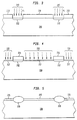
- a substrate 100 is patterned with a pattern layer 110, preferably a photoresist mask, to create an area in the substrate where field oxide regions 120 will be formed.
- Fluorine is implanted into the surface of the substrate 100 as indicated by arrows 115.
- the fluorine atoms are implanted into the surface of the substrate 100 by ion implantation to form fluorine implant regions 112.
- the fluorine atoms are implanted using conventional implantation apparatus, such as ion implantation apparatus by methods known to the person having ordinary skill in the art.
- the fluorine atoms are implanted into the substrate 100 at an amount of from about 1 x 10 11 atoms/cm 2 to about 5 x 10 16 atoms/cm 2 , preferably from about 5 x 10 12 atoms/cm 2 to about 7 x 10 15 atoms/cm 2 .
- the fluorine atoms are implanted at an energy of from about 1 KeV to about 1 MeV, preferably from about 10 KeV to about 50 KeV.
- the implantation energy together with the amount of fluorine atoms implanted determine the depth of the implantation. These three factors, amount, depth and implant energy, affect the amount of growth of the field oxide region 120.
- Field oxide region 120 will preferably have a thickness of from about 1,000 ⁇ to about 10,000 ⁇ .
- Gate oxide layer 125 will have a thickness of from about 20 ⁇ to about 1,000 ⁇ , preferably from about 50 ⁇ to about 500 ⁇ .
- the field oxide region 120 and gate oxide region 125 will have a fluorine content of from about 1 x 10 9 atoms/cm 2 to about 5 x 10 14 atoms/cm 2 , preferably from about 5 x 10 10 atoms/cm 2 to about 7 x 10 13 atoms/cm 2 .
- a second patterned layer (not shown) may be applied over substrate 100 and a fluorine layer may be implanted into the substrate 100 to grow the gate oxide layer 125 in selected regions of the substrate 100.
- a substrate 200 is patterned with a pattern layer 210, preferably a photoresist mask, to create an area in the substrate where the field oxide region 220 (Fig. 5) will be formed.
- Fluorine is implanted into the surface of the substrate 200 as indicated by arrows 215.
- the fluorine atoms are implanted into the surface of the substrate 200 by ion implantation.
- the fluorine atoms are implanted into the substrate 200 at an amount of from about 1 x 10 11 atoms/cm 2 to about 5 x 10 16 atoms/cm 2 , preferably from about 5 x 10 12 atoms/cm 2 to about 7 x 10 15 atoms/cm 2 .
- the fluorine atoms are implanted at an energy of from about 1 KeV to about 1 MeV, preferably from about 10 KeV to about 50 KeV.
- the implantation energy together with the amount of fluorine atoms implanted determine the depth of the implantation.
- the patterned layer 210 is removed.
- a second pattern layer 211 is applied to the substrate over the implanted regions 212.
- Fluorine is implanted into the surface of the substrate 210 as indicated by arrows 215. Again, the fluorine atoms are preferably implanted into the surface of the substrate 200 by ion implantation.
- the fluorine atoms may be implanted into the substrate 200 at an amount of from about 1 x 10 11 atoms/cm 2 to about 5 x 10 16 atoms/cm 2 , preferably from about 5 x 10 12 atoms/cm 2 to about 7 x 10 15 atoms/cm 2 ; however, it is generally understood that the fluorine implantation to form the gate oxide layer 225 (Fig. 5) is implanted at a lower level and to a shallower depth than the fluorine implantation to form field oxide regions 220.
- Field oxide region 220 will preferably have a thickness of from about 1,000 ⁇ to about 10,000 ⁇ .
- Gate oxide layer 225 will have a thickness of from about 20 ⁇ to about 1,000 ⁇ , preferably from about 50 ⁇ to about 500 ⁇ .
- the field oxide region 220 and gate oxide region 2125 will have a fluorine content of from about 1 x 10 9 atoms/cm 2 to about 5 x 10 14 atoms/cm 2 , preferably from about 5 x 10 10 atoms/cm 2 to about 7 x 10 13 atoms/cm 2 .
- the present invention allows the gate oxide layer and the field oxide layer to be grown simultaneously.
- the process according to the present invention may also be used to grow gate oxides of different thicknesses allowing circuit operation at different voltages for different parts of the circuit as shown in Figs. 6-9. It should be understood from these figures that isolation regions may be formed in the device shown in these figures prior to the described processing. While these isolation regions have not depicted here, it is understood that they are within the scope of the present invention.
- a first mask 301 is place over substrate 300 and fluorine is implanted through the openings in the mask 301 at a predetermined dosage and energy level as shown by arrows 315 to form fluorine implantation region 312 as illustrated in Fig. 6.
- the mask 301 is removed and a second mask 302 is then applied and fluorine is then implanted in the openings in the second mask 302 at a predetermined dosage and energy level as shown by arrows 315 to form fluorine implantation region 313 as illustrated in Fig. 7.
- the dosage, energy of implantation and depth of implantation may be varied according to the thickness of the field oxide to be grown over substrate 300. While only two masks and corresponding fluorine implant regions have been illustrated, it should be understood that a plurality of masks and regions of varying fluorine implant dosage and depth may be formed according to the present invention.
- Gate oxide regions 220, 225 will have a thickness of from about 20 ⁇ to about 1,000 ⁇ , preferably from about 50 ⁇ to about 500 ⁇ and a fluorine content of from about 1 x 10 9 atoms/cm 2 to about 5 x 10 14 atoms/cm 2 , preferably from about 5 x 10 10 atoms/cm 2 to about 7 x 10 13 atoms/cm 2 . It should be understood that further processing, such as formation of source/drain regions, deposition of further layers and the like may be performed to arrive at an operable integrated circuit device.
- the present invention improves over the conventional methods for producing gate and other oxides having different thicknesses.
- One conventional method uses multiple oxidation steps where the unwanted oxide is removed by wet chemical etching in between the oxidation steps. This process generally results in a lack of control of at least one of the oxidation thicknesses and it is more difficult to control the differential between the desired thicknesses.
- Another approach is to use a single oxidation step and retard the oxidation of selected areas by nitrogen implantation.
- the present invention overcomes these shortcomings and produces gate oxides of differing thicknesses in a commercially efficient fabrication process.
- Silicon wafers of (100) orientation and 125 mm diameter were doped with boron to a level of nominally 10 15 atoms/cm 2 to arrive at a substrate having a p-type conductivity.
- the wafers were then implanted with F + at implant levels from 5x10 12 to 7x10 15 atoms/cm 2 as shown in Table 1 below.
- the implant energy in the examples was varied between about 10 and 50 KeV.
- the fluorine implanted wafers receiving the various implants were oxidized in one of two processes along with control wafers which were only doped with the boron to form a conductivity type described above.
- One process used a conventional process used to grow 125 ⁇ oxide layers having an ambient of 98% oxygen and 2% HCl at 850°C on unimplanted wafers.
- a second process utilized an ambient of 100% oxygen at a temperature of 750°C.
- the wafers implanted with fluorine exhibited greater growth than the control wafers.
- the wafers implanted with fluorine achieved an oxide thickness of up to 40 ⁇ greater than the control wafers.
- the fluorine implanted wafers also had much greater oxide growth that wafers implanted with silicon ions.
Landscapes
- Formation Of Insulating Films (AREA)
- Metal-Oxide And Bipolar Metal-Oxide Semiconductor Integrated Circuits (AREA)
- Local Oxidation Of Silicon (AREA)
- Element Separation (AREA)
- Insulated Gate Type Field-Effect Transistor (AREA)
Abstract
Description
| IMPLANT | DOPING LEVEL (ions/ cm2) | GATE OXIDE THICKNESS (Å) |
| Fluorine | 7x10¹⁵ | 162.86 |
| Fluorine | 7x10¹⁵ | 163.17 |
| Fluorine | 5x10¹⁵ | 169.29 |
| Fluorine | 5x10¹⁵ | 169.19 |
| Fluorine | 1x10¹⁵ | 134.21 |
| Fluorine | 1x10¹⁵ | 134.45 |
| Control | Control | 129.94 |
| Control | Control | 130.13 |
| Silicon | 1x10¹⁵ | 131.81 |
| Silicon | 1x10¹⁵ | 132.17 |
| Silicon | 5x10¹⁵ | 133.12 |
| Silicon | 5x10¹⁵ | 132.96 |
Claims (31)
- An integrated circuit device having at least one oxide region formed thereon, said oxide region being formed by implanting fluorine into a substrate and thermally treating said substrate to form said oxide layer.
- The device according to claim 1, wherein said oxide layer is an isolation region.
- The device according to claim 1, wherein said oxide layer is a gate oxide layer
- The device according to claim 1, wherein said fluorine is implanted in an amount of from about 1 x 10¹¹ atoms/cm2 to about 5 x 10¹⁶ atoms/cm2.
- The device according to claim 1, wherein said fluorine is implanted in an amount of from about 5 x 10¹² atoms/cm2 to about 7 x 10¹⁵ atoms/cm2.
- The device according to claim 1, wherein said device includes both isolation regions and gate oxide regions formed by implanting fluorine into said substrate and thermally treating said substrate.
- The device according to claim 2, wherein said isolation region has a thickness of from about 1,000Å to about 10,000Å.
- The device according to claim 3, wherein said gate oxide region has a thickness of from about 20Å to about 1,000Å.
- The device according to claim 3, wherein said gate oxide has a thickness of from about 50Å to about 500Å.
- The device according to claim 6, wherein said isolation region has a thickness of from about 1,000Å to about 10,000Å and said gate oxide region has a thickness of from about 20Å to about 1,000Å.
- An integrated circuit device comprising:a material layer which includes a fluorine implant; andat least one oxide layer over said material layer.
- The device according to claim 11, wherein said material layer is a silicon layer.
- The device according to claim 12, wherein said oxide layer is an isolation region.
- The device according to claim 12, wherein said oxide layer is a gate oxide layer
- The device according to claim 11, wherein said fluorine is present in said material layer in an amount of from about 1 x 10⁹ atoms/cm2 to about 5 x 10¹⁴ atoms/cm2.
- The device according to claim 11, wherein said fluorine is present in said material layer in an amount of from about 5 x 10¹⁰ atoms/cm2 to about 7 x 10¹³ atoms/cm2.
- The device according to claim 12, wherein said fluorine is present in said silicon layer in an amount of from about 1 x 10⁹ atoms/cm2 to about 5 x 10¹⁴ atoms/cm2.
- The device according to claim 12, wherein said fluorine is present in said silicon layer in an amount of from about 5 x 10¹⁰ atoms/cm2 to about 7 x 10¹³ atoms/cm2.
- The device according to claim 11, wherein said oxide layer has a thickness of from about 20Å to about 10,000Å.
- The device according to claim 11, wherein said oxide layer is an isolation region.
- The device according to claim 11, wherein said oxide layer is a gate oxide layer
- The device according to claim 20, wherein said isolation region has a thickness of from about 1,000Å to about 10,000Å.
- The device according to claim 21, wherein said gate oxide layer has a thickness of from about 20Å to about 1,000Å.
- The device according to claim 21, wherein said gate oxide has a thickness of from about 50Å to about 500Å.
- The device according to claim 11, wherein said oxide layer includes both isolation regions and gate oxide regions formed by implanting fluorine into said substrate and thermally treating said substrate.
- The device according to claim 25, wherein said isolation region has a thickness of from about 1,000Å to about 10,000Å and said gate oxide region has a thickness of from about 20Å to about 1,000Å.
- The device according to claim 26, wherein said gate oxide region has a thickness of from about 50Å to about 500Å.
- An integrated circuit device having at least a first and second oxide region formed thereon, said oxide regions being formed by implanting fluorine into a substrate in at least a first level, implanting fluorine into said substrate in at lease a second level and thermally treating said substrate to form said first and second oxide layers, wherein said first and second oxide regions have different thicknesses.
- The device according to claim 28, wherein said first and second oxide regions are gate oxide regions.
- The device according to claim 29, wherein said first and second oxide regions are silicon oxide regions.
- The device according to claim 28, wherein said gate oxide regions have a thickness of between about 50Å to about 500Å and wherein said first gate oxide region is larger than said second gate oxide region.
Applications Claiming Priority (2)
| Application Number | Priority Date | Filing Date | Title |
|---|---|---|---|
| US31163399A | 1999-05-14 | 1999-05-14 | |
| US311633 | 1999-05-14 |
Publications (2)
| Publication Number | Publication Date |
|---|---|
| EP1052685A2 true EP1052685A2 (en) | 2000-11-15 |
| EP1052685A3 EP1052685A3 (en) | 2001-11-07 |
Family
ID=23207779
Family Applications (1)
| Application Number | Title | Priority Date | Filing Date |
|---|---|---|---|
| EP00303688A Withdrawn EP1052685A3 (en) | 1999-05-14 | 2000-05-03 | Integrated circuit device having a fluorine implanted oxide layer |
Country Status (3)
| Country | Link |
|---|---|
| EP (1) | EP1052685A3 (en) |
| JP (1) | JP2000357689A (en) |
| KR (1) | KR20010020834A (en) |
Families Citing this family (4)
| Publication number | Priority date | Publication date | Assignee | Title |
|---|---|---|---|---|
| JP5298403B2 (en) * | 2005-10-13 | 2013-09-25 | 富士電機株式会社 | Manufacturing method of semiconductor device |
| JP5228291B2 (en) * | 2006-07-06 | 2013-07-03 | 日産自動車株式会社 | Manufacturing method of semiconductor device |
| JP2008166749A (en) * | 2006-12-05 | 2008-07-17 | Semiconductor Energy Lab Co Ltd | THIN FILM TRANSISTOR, MANUFACTURING METHOD THEREOF, AND SEMICONDUCTOR DEVICE HAVING THE THIN FILM TRANSISTOR |
| JP2009130192A (en) * | 2007-11-26 | 2009-06-11 | Fujitsu Microelectronics Ltd | Manufacturing method of semiconductor device |
Family Cites Families (10)
| Publication number | Priority date | Publication date | Assignee | Title |
|---|---|---|---|---|
| JPS5585068A (en) * | 1978-12-21 | 1980-06-26 | Sony Corp | Preparation of semiconductor device |
| JPS62177930A (en) * | 1986-01-31 | 1987-08-04 | Toshiba Corp | High speed oxidation method for semiconductor substrate |
| JPH03163876A (en) * | 1989-11-22 | 1991-07-15 | Hitachi Ltd | Semiconductor device |
| JPH0574762A (en) * | 1991-09-17 | 1993-03-26 | Oki Electric Ind Co Ltd | Insulating film formation method |
| JP3453764B2 (en) * | 1992-02-04 | 2003-10-06 | 富士通株式会社 | Method for manufacturing semiconductor device |
| JPH07240409A (en) * | 1994-02-28 | 1995-09-12 | Fuji Electric Co Ltd | Method for manufacturing silicon carbide semiconductor device |
| JPH0955380A (en) * | 1995-08-11 | 1997-02-25 | Ricoh Co Ltd | Method for manufacturing MOS semiconductor device |
| JPH09237784A (en) * | 1996-02-29 | 1997-09-09 | Sanyo Electric Co Ltd | Element isolation method |
| JPH1064898A (en) * | 1996-08-16 | 1998-03-06 | Texas Instr Japan Ltd | Method for manufacturing semiconductor device |
| JP3194370B2 (en) * | 1998-05-11 | 2001-07-30 | 日本電気株式会社 | Semiconductor device and manufacturing method thereof |
-
2000
- 2000-05-03 EP EP00303688A patent/EP1052685A3/en not_active Withdrawn
- 2000-05-12 KR KR1020000025276A patent/KR20010020834A/en not_active Withdrawn
- 2000-05-15 JP JP2000142468A patent/JP2000357689A/en active Pending
Also Published As
| Publication number | Publication date |
|---|---|
| JP2000357689A (en) | 2000-12-26 |
| EP1052685A3 (en) | 2001-11-07 |
| KR20010020834A (en) | 2001-03-15 |
Similar Documents
| Publication | Publication Date | Title |
|---|---|---|
| US4717683A (en) | CMOS process | |
| US6358865B2 (en) | Oxidation of silicon using fluorine implant | |
| US5234850A (en) | Method of fabricating a nitride capped MOSFET for integrated circuits | |
| US5196367A (en) | Modified field isolation process with no channel-stop implant encroachment | |
| KR100411985B1 (en) | Method for patterning a buried oxide thickness for a separation by implanted oxygen (simox) process | |
| JP3007437B2 (en) | Method for manufacturing CMOS device | |
| US6890833B2 (en) | Trench isolation employing a doped oxide trench fill | |
| US4743563A (en) | Process of controlling surface doping | |
| US6413881B1 (en) | Process for forming thin gate oxide with enhanced reliability by nitridation of upper surface of gate of oxide to form barrier of nitrogen atoms in upper surface region of gate oxide, and resulting product | |
| US6069054A (en) | Method for forming isolation regions subsequent to gate formation and structure thereof | |
| US6852610B2 (en) | Semiconductor device and method for manufacturing the same | |
| JPS61237422A (en) | Manufacture of semiconductor device | |
| US5739580A (en) | Oxide formed in semiconductor substrate by implantation of substrate with a noble gas prior to oxidation | |
| US5106768A (en) | Method for the manufacture of CMOS FET by P+ maskless technique | |
| US5208181A (en) | Locos isolation scheme for small geometry or high voltage circuit | |
| US6686255B2 (en) | Amorphizing ion implant local oxidation of silicon (LOCOS) method for forming an isolation region | |
| US5476800A (en) | Method for formation of a buried layer for a semiconductor device | |
| US6762112B2 (en) | Method for manufacturing isolating structures | |
| US6455405B1 (en) | Using implantation method to control gate oxide thickness on dual oxide semiconductor devices | |
| KR20010020834A (en) | Integrated circuit device having a fluorine implanted oxide layer | |
| US20020036324A1 (en) | Hydrogen anneal before gate oxidation | |
| EP0367729A2 (en) | Process for forming trench isolation structures in a silicon substrate for CMOS and NMOS devices | |
| CA1194616A (en) | Process for forming a shallow, high-concentration impurity layer in a semiconductor body | |
| US7361562B2 (en) | Method of manufacturing semiconductor device | |
| US20050014344A1 (en) | Method of forming well in semiconductor device |
Legal Events
| Date | Code | Title | Description |
|---|---|---|---|
| PUAI | Public reference made under article 153(3) epc to a published international application that has entered the european phase |
Free format text: ORIGINAL CODE: 0009012 |
|
| AK | Designated contracting states |
Kind code of ref document: A2 Designated state(s): AT BE CH CY DE DK ES FI FR GB GR IE IT LI LU MC NL PT SE |
|
| AX | Request for extension of the european patent |
Free format text: AL;LT;LV;MK;RO;SI |
|
| PUAL | Search report despatched |
Free format text: ORIGINAL CODE: 0009013 |
|
| AK | Designated contracting states |
Kind code of ref document: A3 Designated state(s): AT BE CH CY DE DK ES FI FR GB GR IE IT LI LU MC NL PT SE |
|
| AX | Request for extension of the european patent |
Free format text: AL;LT;LV;MK;RO;SI |
|
| AKX | Designation fees paid | ||
| REG | Reference to a national code |
Ref country code: DE Ref legal event code: 8566 |
|
| STAA | Information on the status of an ep patent application or granted ep patent |
Free format text: STATUS: THE APPLICATION IS DEEMED TO BE WITHDRAWN |
|
| 18D | Application deemed to be withdrawn |
Effective date: 20020508 |