EP1052680B1 - Pulse mode electron generator - Google Patents
Pulse mode electron generator Download PDFInfo
- Publication number
- EP1052680B1 EP1052680B1 EP00400835A EP00400835A EP1052680B1 EP 1052680 B1 EP1052680 B1 EP 1052680B1 EP 00400835 A EP00400835 A EP 00400835A EP 00400835 A EP00400835 A EP 00400835A EP 1052680 B1 EP1052680 B1 EP 1052680B1
- Authority
- EP
- European Patent Office
- Prior art keywords
- cathode
- grid
- voltage
- emission
- electrons
- Prior art date
- Legal status (The legal status is an assumption and is not a legal conclusion. Google has not performed a legal analysis and makes no representation as to the accuracy of the status listed.)
- Expired - Lifetime
Links
Images

Classifications
-
- H—ELECTRICITY
- H01—ELECTRIC ELEMENTS
- H01J—ELECTRIC DISCHARGE TUBES OR DISCHARGE LAMPS
- H01J37/00—Discharge tubes with provision for introducing objects or material to be exposed to the discharge, e.g. for the purpose of examination or processing thereof
- H01J37/02—Details
- H01J37/04—Arrangements of electrodes and associated parts for generating or controlling the discharge, e.g. electron-optical arrangement, ion-optical arrangement
- H01J37/06—Electron sources; Electron guns
- H01J37/073—Electron guns using field emission, photo emission, or secondary emission electron sources
-
- G—PHYSICS
- G09—EDUCATION; CRYPTOGRAPHY; DISPLAY; ADVERTISING; SEALS
- G09G—ARRANGEMENTS OR CIRCUITS FOR CONTROL OF INDICATING DEVICES USING STATIC MEANS TO PRESENT VARIABLE INFORMATION
- G09G3/00—Control arrangements or circuits, of interest only in connection with visual indicators other than cathode-ray tubes
- G09G3/20—Control arrangements or circuits, of interest only in connection with visual indicators other than cathode-ray tubes for presentation of an assembly of a number of characters, e.g. a page, by composing the assembly by combination of individual elements arranged in a matrix no fixed position being assigned to or needed to be assigned to the individual characters or partial characters
- G09G3/22—Control arrangements or circuits, of interest only in connection with visual indicators other than cathode-ray tubes for presentation of an assembly of a number of characters, e.g. a page, by composing the assembly by combination of individual elements arranged in a matrix no fixed position being assigned to or needed to be assigned to the individual characters or partial characters using controlled light sources
-
- H—ELECTRICITY
- H01—ELECTRIC ELEMENTS
- H01J—ELECTRIC DISCHARGE TUBES OR DISCHARGE LAMPS
- H01J3/00—Details of electron-optical or ion-optical arrangements or of ion traps common to two or more basic types of discharge tubes or lamps
- H01J3/02—Electron guns
- H01J3/021—Electron guns using a field emission, photo emission, or secondary emission electron source
- H01J3/022—Electron guns using a field emission, photo emission, or secondary emission electron source with microengineered cathode, e.g. Spindt-type
-
- H—ELECTRICITY
- H01—ELECTRIC ELEMENTS
- H01J—ELECTRIC DISCHARGE TUBES OR DISCHARGE LAMPS
- H01J49/00—Particle spectrometers or separator tubes
- H01J49/02—Details
- H01J49/10—Ion sources; Ion guns
Definitions
- the present invention relates to electron generators comprising an electron-emitting micropoint field-emitting cathode associated with a gate biased by gate positive biasing means, with an anode attracting electrons emitted by the cathode.
- micropoint field emission cathodes As a electron generator, electron-emitting micropoint field emission cathodes have been developed for some years (see, for example, document FR 2 734 076A), in which electrically conductive micropoints are produced on a substrate. suitable conductor and recessed in cavities of an insulating layer covering the substrate, with their end flush with a positively polarized gate and having openings facing each cavity. The sharp shape of the peaks of the microtips produces a local electric field amplification effect which promotes the emission of electrons at ambient temperature and makes it possible to obtain this emission from a threshold voltage of the order of 50 to 100. volts depending on the constitution of the micropoint network.
- Such field emission cathodes have a particularly good energy efficiency, better than that of a traditional electron source in the form of a tungsten filament heated between 1000 and 2000 ° C and producing an electron emission by thermoelectronic effect. It is known that the power involved in emitting the electrons is of the order of 10 watts for a heated tungsten filament, whereas this power is of the order of 0.2 watts for a field emission cathode.
- Another advantage of field emission cathodes is their rapid reaction, both at the beginning of electron emission and at the end of emission.
- the gate is polarized by a zero voltage, that is to say, it is at the potential of the cathode.
- the gate is biased to a positive voltage greater than the cathode emission threshold voltage.
- micropoint field emission cathodes are satisfactory for electron generation in steady state or low frequency modulated mode.
- the electron packets In certain applications, for example for time-of-flight mass spectrometers, it is necessary to generate an intermittent flow of electrons in the form of electron packets of the shortest possible duration, of the order of one nanosecond, and the electron packets must contain as many electrons as possible.
- the intermittent flow of electrons is equivalent to a current of 1 to 2 mA.
- the field emission cathodes require having polarization generators capable of polarizing the gate with electrical pulses of the order of one nanosecond to a sufficient amplitude to reach the threshold emission voltage of the cathode.
- Such electrical impulses of great amplitude and of short duration are difficult to achieve, and the powers involved are not negligible because of the consumption of electrical energy in the capacitive element constituted by the field emission cathode.
- -Even of which the frames are constituted by the grid on the one hand, and by the substrate and the microtips on the other hand. It will be noted that the power consumed in this capacitive element increases as the square of the AC voltage applied to its terminals, and is proportional to its frequency.
- the problem proposed by the present invention is to design a new field emission cathode pulsed electron pulse generator structure that substantially reduces the power involved in pulsed mode, and makes it possible to considerably facilitate the control of the cathode by a electric pulse generator easier to achieve.
- Another object of the invention is to improve the pulse regime of the electron generator by reducing the duration of the rise and fall fronts of the electron pulses.
- the bias voltage value is modified by an amplitude equal to the difference between the emission voltage value and the transmission voltage value. idle voltage value. This amplitude is therefore only a fraction of the emission voltage value.
- the power involved in each impulse cycle is therefore greatly reduced, since only this difference between the transmission voltage and the rest voltage intervenes in the calculation of the power, and intervenes squared. Also, it is easier to realize a steep-edge pulse whose amplitude is equal only to the difference between the emission voltage and the quiescent voltage. This simplifies the realization of the gate bias generator, and this improves the waveform of the electron packet emitted by the generator.
- the idle voltage value is slightly lower than the cathode emission threshold voltage. This produces a generator whose structure is particularly simple, having no element other than those usually used in field emitting microtip cathodes emitting electron.
- a transparent repulsive grid interposed between the cathode gate and the anode, polarized slightly below the cathode emission threshold voltage, to push back the cathode streams towards the cathode. electrons having insufficient energy during the steps of non-electron emission, and to pass electron streams having sufficient energy during the electron emission steps.
- the gate positive biasing means generates a gate bias voltage comprising a permanent positive prepolarization voltage over which is superimposed a positive bias voltage bias component.
- the gate positive biasing means may comprise a permanent positive prepolarization voltage generator, delivering said permanent positive prepolarization voltage, in series with a positive pulse voltage generator outputting said component. positive impulse bias voltage.
- said positive impulse bias voltage component has an amplitude of only a few volts. Indeed, it is easy to generate a pulse having a duration of one nanosecond and an amplitude of about 10 volts.
- the flow of electrons emitted by such generators has substantially the same pace as the signal constituted by said positive impulse bias voltage component.
- an electron pulse generator according to the present invention comprises a field emission cathode 1 for generating an electron flow 2 towards an anode 3.
- the field emission cathode 1 comprises, in known manner, a conductive substrate 4, for example made of silicon, having an active face 5 on which microtips 6-11 are arranged.
- the active face 5 is covered with an insulating layer 12, for example silicon oxide, separating it from a conductive grid 13.
- the microtips 6-11 are housed in respective cavities 14-19 formed in the insulating layer 12 and communicating in the direction of the anode 3 by corresponding openings provided in the grid 13. The tips of the microtips 6-11 come out flush with each other. the grid surface 13.
- the size of the cavities 14-19, and therefore the size of the microtips 6-11, is of the order of one micron in height and in width.
- Microtip arrays are generally produced whose density is in the order of 10,000 to 100,000 microtips per mm 2 .
- Positive gate polarization means 20 are connected between the substrate 4 and the gate 13, to ensure the positive bias of the gate 13.
- the gate positive polarization means 20 comprise a permanent positive prepolarization voltage generator 21, delivering a permanent positive prepolarization voltage V21, in series with a positive pulse voltage generator 22 delivering a pulse component positive V22 bias voltage.
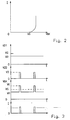
- FIG. 3 illustrates the permanent positive prepolarization voltage V21, in the form of a DC voltage VR, and the positive bias voltage component V22, in the form of rectangular pulses of amplitude VI.
- the electric current I corresponding to the electron flux emitted by the cathode is zero as long as the gate bias voltage VGK is below an emission threshold VS of the cathode. Beyond the emission threshold VS, the bias voltage VGK of the gate with respect to the cathode produces an electron current I which increases exponentially as a function of the voltage.
- the threshold voltage VS is generally of the order of 50 to 100 volts, depending on the constitution of the microtip array of the cathode.
- a quiescent voltage value VR is chosen which, during the non-electron emission steps, remains only slightly less than the active bias voltage VA of gate 13.
- the active bias voltage VA of gate 13 as the bias voltage VGK from which the anode 3 receives a significant flow of electrons from the cathode 1.
- a transmission voltage value VE is chosen which, during the transmission steps of electrons, is greater than said active bias voltage VA gate 13.
- the voltage threshold voltage VA of the cathode 1 is selected as the active bias voltage value VA.
- the idle voltage value VR can then be chosen slightly smaller than the voltage of emission threshold VS of the cathode 1.
- a transparent repulsive grating 23 as illustrated in FIG. 1.
- the transparent repulsive grating 23 is interposed in the electron flow between the cathode gate 13 and the anode 3, and is biased by a generator 24 slightly below the transmission threshold voltage VS of the cathode 1.
- the gate transparent repulsive 23 pushes back towards the cathode 1 the electron flows 25 having insufficient energy during the non-electron emission steps, while it allows the electron fluxes 2 having a sufficient energy conferred by the polarization voltage to pass; VE emission during the electron emission steps.
- a pulsed electron generator according to the invention can advantageously be used as an electron source in a time-of-flight mass spectrometer.
Abstract
Description
La présente invention concerne les générateurs d'électrons comprenant une cathode à émission de champ à micropointes émettrices d'électrons associées à une grille polarisée par des moyens de polarisation positive de grille, avec une anode attirant les électrons émis par la cathode.The present invention relates to electron generators comprising an electron-emitting micropoint field-emitting cathode associated with a gate biased by gate positive biasing means, with an anode attracting electrons emitted by the cathode.
Comme générateur d'électrons, on a développé depuis quelques années des cathodes à émission de champ à micropointes émettrices d'électrons (voir par exemple le document FR 2 734 076A), dans lesquelles des micropointes conductrices de l'électricité sont réalisées sur un substrat conducteur approprié et encastrées dans des cavités d'une couche isolante recouvrant le substrat, avec leur extrémité venant en affleurement d'une grille polarisée positivement et comportant des ouvertures au regard de chaque cavité. La forme acérée des sommets des micropointes produit un effet d'amplification locale de champ électrique qui favorise l'émission des électrons à température ambiante et permet d'obtenir cette émission à partir d'une tension de seuil de l'ordre de 50 à 100 volts en fonction de la constitution du réseau de micropointes.As a electron generator, electron-emitting micropoint field emission cathodes have been developed for some years (see, for example, document FR 2 734 076A), in which electrically conductive micropoints are produced on a substrate. suitable conductor and recessed in cavities of an insulating layer covering the substrate, with their end flush with a positively polarized gate and having openings facing each cavity. The sharp shape of the peaks of the microtips produces a local electric field amplification effect which promotes the emission of electrons at ambient temperature and makes it possible to obtain this emission from a threshold voltage of the order of 50 to 100. volts depending on the constitution of the micropoint network.
De telles cathodes à émission de champ présentent notamment un bon rendement énergétique, meilleur que celui d'une source d'électrons traditionnelle sous forme d'un filament de tungstène chauffé entre 1 000 et 2 000°C et produisant une émission d'électrons par effet thermoélectronique. On sait que la puissance mise en jeu pour émettre les électrons est de l'ordre de 10 watts pour un filament de tungstène chauffé, alors que cette puissance est de l'ordre de 0,2 watts pour une cathode à émission de champs.Such field emission cathodes have a particularly good energy efficiency, better than that of a traditional electron source in the form of a tungsten filament heated between 1000 and 2000 ° C and producing an electron emission by thermoelectronic effect. It is known that the power involved in emitting the electrons is of the order of 10 watts for a heated tungsten filament, whereas this power is of the order of 0.2 watts for a field emission cathode.
Un autre avantage des cathodes à émission de champ est leur rapidité de réaction, aussi bien en début d'émission d'électrons qu'en fin d'émission.Another advantage of field emission cathodes is their rapid reaction, both at the beginning of electron emission and at the end of emission.
Dans les dispositifs connus, au cours des étapes de repos ou de non émission d'électrons, la grille est polarisée par une tension nulle, c'est-à-dire qu'elle se trouve au potentiel de la cathode. Au cours des étapes d'émission d'électrons, la grille est polarisée à une tension positive supérieure à la tension de seuil d'émission de la cathode.In known devices, during the resting or non-electron emission steps, the gate is polarized by a zero voltage, that is to say, it is at the potential of the cathode. During the electron emission steps, the gate is biased to a positive voltage greater than the cathode emission threshold voltage.
Ces cathodes à émission de champ à micropointes émettrices d'électrons donnent satisfaction pour la génération d'électrons en régime continu ou en régime modulé à basse fréquence.These electron-emitting micropoint field emission cathodes are satisfactory for electron generation in steady state or low frequency modulated mode.
Dans certaines applications, par exemple pour les spectromètres de masse à temps de vol, on a besoin de générer un flux intermittent d'électrons sous forme de paquets d'électrons de durée la plus faible possible, de l'ordre de la nanoseconde, et les paquets d'électrons doivent contenir le maximum d'électrons possible. Le flux intermittent d'électrons équivaut à un courant de 1 à 2 mA.In certain applications, for example for time-of-flight mass spectrometers, it is necessary to generate an intermittent flow of electrons in the form of electron packets of the shortest possible duration, of the order of one nanosecond, and the electron packets must contain as many electrons as possible. The intermittent flow of electrons is equivalent to a current of 1 to 2 mA.
Dans ce cas, les cathodes à émission de champ nécessitent de disposer de générateurs de polarisation capables de polariser la grille avec des impulsions électriques de l'ordre de la nanoseconde selon une amplitude suffisante pour atteindre la tension de seuil d'émission de la cathode. De telles impulsions électriques de grande amplitude et de faible durée s'avèrent difficiles à réaliser, et les puissances mises en jeu sont non négligeables à cause de la consommation d'énergie électrique dans l'élément capacitif constitué par la cathode à émission de champ elle-même dont les armatures sont constituées par la grille d'une part, et par le substrat et les micropointes d'autre part. On notera que la puissance consommée dans cet élément capacitif augmente comme le carré de la tension alternative appliquée à ses bornes, et est proportionnelle à sa fréquence.In this case, the field emission cathodes require having polarization generators capable of polarizing the gate with electrical pulses of the order of one nanosecond to a sufficient amplitude to reach the threshold emission voltage of the cathode. Such electrical impulses of great amplitude and of short duration are difficult to achieve, and the powers involved are not negligible because of the consumption of electrical energy in the capacitive element constituted by the field emission cathode. -Even of which the frames are constituted by the grid on the one hand, and by the substrate and the microtips on the other hand. It will be noted that the power consumed in this capacitive element increases as the square of the AC voltage applied to its terminals, and is proportional to its frequency.
Le problème proposé par la présente invention est de concevoir une nouvelle structure de générateur impulsionnel d'électrons à cathode à émission de champ permettant de réduire sensiblement la puissance mise en jeu en régime impulsionnel, et permettant de faciliter considérablement la commande de la cathode par un générateur d'impulsions électriques plus facile à réaliser.The problem proposed by the present invention is to design a new field emission cathode pulsed electron pulse generator structure that substantially reduces the power involved in pulsed mode, and makes it possible to considerably facilitate the control of the cathode by a electric pulse generator easier to achieve.
Un autre objet de l'invention est d'améliorer le régime impulsionnel du générateur d'électrons, en réduisant la durée des fronts de montée et de descente des impulsions d'électrons.Another object of the invention is to improve the pulse regime of the electron generator by reducing the duration of the rise and fall fronts of the electron pulses.
Pour atteindre ces objets ainsi que d'autres, l'invention prévoit un générateur impulsionnel d'électrons, comprenant une cathode à émission de champ à micropointes émettrices d'électrons associées à une grille polarisée par des moyens de polarisation positive de grille, avec une anode attirant les électrons émis par la cathode, et dans lequel les moyens de polarisation positive de grille génèrent une tension de polarisation de grille ayant :
- une valeur de tension de repos qui, pendant les étapes de non émission d'électrons, reste seulement légèrement inférieure à la tension de polarisation active de grille à partir de laquelle l'anode reçoit un flux non négligeable d'électrons provenant de la cathode,
- une valeur de tension d'émission qui, pendant les étapes d'émission d'électrons, est supérieure à ladite tension de polarisation active de grille.
- a quiescent voltage value which, during the non-electron emission steps, remains only slightly less than the active gate bias voltage from which the anode receives a sizeable flow of electrons from the cathode,
- an emission voltage value which, during the electron emission steps, is greater than said active gate bias voltage.
On comprend que, entre l'étape de non émission d'électrons et l'étape d'émission d'électrons, la valeur de tension de polarisation est modifiée selon une amplitude égale à la différence entre la valeur de tension d'émission et la valeur de tension de repos. Cette amplitude est donc une fraction seulement de la valeur de tension d'émission. La puissance mise en jeu à chaque cycle impulsionnel est donc fortement réduite, puisque seule cette différence entre la tension d'émission et la tension de repos intervient dans le calcul de la puissance, et intervient au carré. Egalement, il est plus facile de réaliser une impulsion à fronts raides dont l'amplitude est égale seulement à la différence entre la tension d'émission et la tension de repos. Cela simplifie la réalisation du générateur de polarisation de grille, et cela améliore la forme d'onde du paquet d'électrons émis par le générateur.It will be understood that, between the non-electron emission step and the electron emission step, the bias voltage value is modified by an amplitude equal to the difference between the emission voltage value and the transmission voltage value. idle voltage value. This amplitude is therefore only a fraction of the emission voltage value. The power involved in each impulse cycle is therefore greatly reduced, since only this difference between the transmission voltage and the rest voltage intervenes in the calculation of the power, and intervenes squared. Also, it is easier to realize a steep-edge pulse whose amplitude is equal only to the difference between the emission voltage and the quiescent voltage. This simplifies the realization of the gate bias generator, and this improves the waveform of the electron packet emitted by the generator.
Selon un mode de réalisation, la valeur de tension de repos est légèrement inférieure à la tension de seuil d'émission de la cathode. On réalise ainsi un générateur dont la structure est particulièrement simple, ne comportant aucun élément autre que ceux habituellement utilisés dans les cathodes à émission de champ à micropointes émettrices d'électrons.According to one embodiment, the idle voltage value is slightly lower than the cathode emission threshold voltage. This produces a generator whose structure is particularly simple, having no element other than those usually used in field emitting microtip cathodes emitting electron.
En alternative ou en complément, on peut prévoir une grille répulsive transparente interposée entre la grille de cathode et l'anode, polarisée légèrement au-dessous de la tension de seuil d'émission de la cathode, pour repousser vers la cathode les flux d'électrons ayant une énergie insuffisante pendant les étapes de non émission d'électrons, et pour laisser passer les flux d'électrons ayant une énergie suffisante pendant les étapes d'émission d'électrons.Alternatively or additionally, it is possible to provide a transparent repulsive grid interposed between the cathode gate and the anode, polarized slightly below the cathode emission threshold voltage, to push back the cathode streams towards the cathode. electrons having insufficient energy during the steps of non-electron emission, and to pass electron streams having sufficient energy during the electron emission steps.
Cela permet d'inhiber de façon plus certaine toute émission d'électrons lors des étapes de non émission, et éventuellement d'utiliser une tension de repos légèrement supérieure pour la polarisation permanente de grille.This makes it possible to more definitely inhibit any emission of electrons during the non-emission steps, and possibly to use a slightly higher resting voltage for the permanent grid bias.
En pratique, on peut prévoir que les moyens de polarisation positive de grille génèrent une tension de polarisation de grille comprenant une tension de prépolarisation positive permanente à laquelle est superposée une composante impulsionnelle positive de tension de polarisation.In practice, it can be provided that the gate positive biasing means generates a gate bias voltage comprising a permanent positive prepolarization voltage over which is superimposed a positive bias voltage bias component.
Pour réaliser de façon simple le générateur de polarisation de grille, les moyens de polarisation positive de grille peuvent comprendre un générateur de tension de prépolarisation positive permanente, délivrant ladite tension de prépolarisation positive permanente, en série avec un générateur de tension impulsionnelle positive délivrant ladite composante impulsionnelle positive de tension de polarisation.In order to simply realize the gate bias generator, the gate positive biasing means may comprise a permanent positive prepolarization voltage generator, delivering said permanent positive prepolarization voltage, in series with a positive pulse voltage generator outputting said component. positive impulse bias voltage.
De préférence, ladite composante impulsionnelle positive de tension de polarisation a une amplitude de quelques volts seulement. En effet, il est facile de générer une impulsion ayant une durée de une nanoseconde et une amplitude d'environ 10 volts.Preferably, said positive impulse bias voltage component has an amplitude of only a few volts. Indeed, it is easy to generate a pulse having a duration of one nanosecond and an amplitude of about 10 volts.
Le flux d'électrons émis par de tels générateurs a sensiblement la même allure que le signal constitué par ladite composante impulsionnelle positive de tension de polarisation.The flow of electrons emitted by such generators has substantially the same pace as the signal constituted by said positive impulse bias voltage component.
D'autres objets, caractéristiques et avantages de la présente invention ressortiront de la description suivante de modes de réalisation particuliers, faite en relation avec les figures jointes, parmi lesquelles:
- la figure 1 est une vue schématique montrant un générateur impulsionnel d'électrons selon un mode de réalisation de la présente invention;
- la figure 2 illustre les caractéristiques tension / courant d'une cathode à émission de champ ; et
- la figure 3 illustre la constitution de la tension de polarisation de grille, et le courant électrique correspondant au flux d'électrons qui en résulte.
- Fig. 1 is a schematic view showing a pulsed electron generator according to an embodiment of the present invention;
- FIG. 2 illustrates the voltage / current characteristics of a field emission cathode; and
- Figure 3 illustrates the constitution of the gate bias voltage, and the electric current corresponding to the resulting electron flow.
En se référant à la figure 1, un générateur impulsionnel d'électrons selon la présente invention comprend une cathode à émission de champ 1, pour générer un flux d'électrons 2 en direction d'une anode 3.Referring to FIG. 1, an electron pulse generator according to the present invention comprises a
La cathode à émission de champ 1 comprend, de façon connue, un substrat conducteur 4, par exemple en silicium, ayant une face active 5 sur laquelle sont disposées des micropointes 6-11. La face active 5 est recouverte d'une couche isolante 12, par exemple en oxyde de silicium, la séparant d'une grille 13 conductrice. Les micropointes 6-11 sont logées dans des cavités respectives 14-19 ménagées dans la couche isolante 12 et communiquant en direction de l'anode 3 par des ouvertures correspondantes prévues dans la grille 13. Les pointes des micropointes 6-11 viennent en affleurement de la surface de grille 13.The
La dimension des cavités 14-19, et donc la dimension des micropointes 6-11, est de l'ordre du micron en hauteur et en largeur. On réalise généralement des réseaux de micropointes dont la densité est de l'ordre de 10 000 à 100 000 micropointes par mm2.The size of the cavities 14-19, and therefore the size of the microtips 6-11, is of the order of one micron in height and in width. Microtip arrays are generally produced whose density is in the order of 10,000 to 100,000 microtips per mm 2 .
Des moyens de polarisation positive de grille 20 sont connectés entre le substrat 4 et la grille 13, pour assurer la polarisation positive de la grille 13.Positive gate polarization means 20 are connected between the substrate 4 and the
Dans la réalisation illustrée sur la figure, les moyens de polarisation positive de grille 20 comprennent un générateur de tension de prépolarisation positive permanente 21, délivrant une tension de prépolarisation positive permanente V21, en série avec un générateur de tension impulsionnelle positive 22 délivrant une composante impulsionnelle positive V22 de tension de polarisation. Par exemple, la figure 3 illustre la tension de prépolarisation positive permanente V21, sous forme d'une tension continue VR, et la composante impulsionnelle V22 positive de tension de polarisation, sous forme d'impulsions rectangulaires d'amplitude VI.In the embodiment illustrated in the figure, the gate positive polarization means 20 comprise a permanent positive
Le troisième graphe de la figure 3 illustre la tension de polarisation de grille VGK résultant de la somme de la tension V21 et de la tension V22, et comportant une valeur de tension de repos VR et une valeur de tension d'émission VE, avec VE = VR + VI.The third graph of FIG. 3 illustrates the gate bias voltage VGK resulting from the sum of the voltage V21 and the voltage V22, and comprising a rest voltage value VR and a transmission voltage value VE, with VE = VR + VI.
En se référant à la figure 2, illustrant la caractéristique courant / tension d'une cathode à émission de champ, on voit que le courant électrique I correspondant au flux d'électrons émis par la cathode est nul tant que la tension de polarisation de grille VGK est inférieure à un seuil d'émission VS de la cathode. Au-delà du seuil d'émission VS, la tension de polarisation VGK de la grille par rapport à la cathode produit un courant d'électrons I qui augmente exponentiellement en fonction de la tension. La tension de seuil VS est généralement de l'ordre de 50 à 100 volts, dépendant de la constitution du réseau de micropointes de la cathode.Referring to FIG. 2, illustrating the current / voltage characteristic of a field emission cathode, it can be seen that the electric current I corresponding to the electron flux emitted by the cathode is zero as long as the gate bias voltage VGK is below an emission threshold VS of the cathode. Beyond the emission threshold VS, the bias voltage VGK of the gate with respect to the cathode produces an electron current I which increases exponentially as a function of the voltage. The threshold voltage VS is generally of the order of 50 to 100 volts, depending on the constitution of the microtip array of the cathode.
Selon la présente invention, on choisit une valeur de tension de repos VR qui, pendant les étapes de non émission d'électrons, reste seulement légèrement inférieure à la tension de polarisation active VA de grille 13. On définit la tension de polarisation active VA de grille 13 comme étant la tension de polarisation VGK à partir de laquelle l'anode 3 reçoit un flux non négligeable d'électrons provenant de la cathode 1. Et on choisit une valeur de tension d'émission VE qui, pendant les étapes d'émission d'électrons, est supérieure à ladite tension de polarisation active VA de grille 13.According to the present invention, a quiescent voltage value VR is chosen which, during the non-electron emission steps, remains only slightly less than the active bias voltage VA of
Selon un mode de réalisation simplifié, on choisit comme valeur de tension de polarisation active VA la tension de seuil d'émission VS de la cathode 1. En pratique, la valeur de tension de repos VR peut alors être choisie légèrement inférieure à la tension de seuil d'émission VS de la cathode 1.According to a simplified embodiment, the voltage threshold voltage VA of the
Si nécessaire, pour annuler de façon certaine le flux d'électrons pendant les périodes de repos, on peut également prévoir une grille répulsive transparente 23 telle qu'illustrée sur la figure 1. La grille répulsive transparente 23 est interposée dans le flux d'électrons entre la grille 13 de cathode et l'anode 3, et est polarisée par un générateur 24 légèrement au-dessous de la tension de seuil d'émission VS de la cathode 1. Ainsi, la grille répulsive transparente 23 repousse vers la cathode 1 les flux d'électrons 25 ayant une énergie insuffisante pendant les étapes de non émission d'électrons, tandis qu'elle laisse passer les flux d'électrons 2 ayant une énergie suffisante conférée par la tension de polarisation d'émission VE pendant les étapes d'émission d'électrons.If necessary, to undoubtedly cancel the flow of electrons during the rest periods, it is also possible to provide a transparent
Dans ce mode de réalisation à grille répulsive transparente 23, on peut choisir une tension de polarisation active VA légèrement supérieure à la tension de seuil d'émission VS de la cathode 1.In this embodiment with a transparent
Dans tous les modes de réalisation, on trouve avantage à prévoir une composante impulsionnelle positive V22 de tension de polarisation dont l'amplitude VI est de quelques volts seulement.In all embodiments, it is advantageous to provide a positive impulse voltage component V22 of bias voltage whose amplitude VI is only a few volts.
Un générateur impulsionnel d'électrons selon l'invention peut avantageusement être utilisé comme source d'électrons dans un spectromètre de masse à temps de vol.A pulsed electron generator according to the invention can advantageously be used as an electron source in a time-of-flight mass spectrometer.
La présente invention n'est pas limitée aux modes de réalisation qui ont été explicitement décrits, mais elle en inclut les diverses variantes et généralisations qui sont à la portée de l'homme du métier.The present invention is not limited to the embodiments that have been explicitly described, but it includes the various variants and generalizations that are within the reach of those skilled in the art.
Claims (7)
- A pulse mode electron generator including a field emission cathode (1) with electron-emitting micropoints (6-11) associated with a grid (13) biased by means (20) for positively biasing the grid and an anode (3) attracting electrons emitted by the cathode (1), characterized in that the means (20) for positively biasing the grid generate a grid bias voltage (VGK) taking:- a rest voltage value (VR) which, during non-emission of electrons, remains only slightly lower than the active bias voltage of the grid (13) from which the anode (3) receives a non-negligible flow of electrons from the cathode (1), or- an emission voltage value (VE) which, during emission of electrons, is higher than said active bias voltage of the grid (13).
- A generator according to claim 1, characterized in that said rest voltage (VR) is slightly lower than the emission threshold voltage (VS) of the cathode (1).
- A generator according to either claim 1 or claim 2, characterized in that a transparent repulsive grid (23) is placed between the cathode grid (13) and the anode (3) and is biased to a voltage slightly lower than the emission threshold voltage (VS) of the cathode (1) in order to repel towards the cathode (1) electrons (25) having insufficient energy during non-emission of electrons and to allow through electrons (2) having sufficient energy during emission of electrons.
- A generator according to any one of claims 1 to 3, characterized in that the means (20) for positively biasing the grid generate a grid bias voltage (VGK) comprising a permanent positive pre-bias voltage (V21) on which is superimposed a positive bias voltage pulse component (V22).
- A generator according to claim 4, characterized in that the means (20) for positively biasing the grid include a permanent positive pre-bias voltage generator (21) delivering said permanent positive pre-bias voltage (V21) and in series with a positive pulse voltage generator (22) delivering said positive bias voltage pulse component (V22).
- A generator according to either claim 4 or claim 5, characterized in that said positive bias voltage pulse component (V22) has an amplitude (VI) of only a few volts.
- A time-of-flight mass spectrometer, characterized in that it includes a pulse mode electron generator according to any of claims 1 to 6.
Applications Claiming Priority (2)
| Application Number | Priority Date | Filing Date | Title |
|---|---|---|---|
| FR9905087A FR2792771B1 (en) | 1999-04-22 | 1999-04-22 | PULSE ELECTRON GENERATOR |
| FR9905087 | 1999-04-22 |
Publications (2)
| Publication Number | Publication Date |
|---|---|
| EP1052680A1 EP1052680A1 (en) | 2000-11-15 |
| EP1052680B1 true EP1052680B1 (en) | 2007-01-03 |
Family
ID=9544731
Family Applications (1)
| Application Number | Title | Priority Date | Filing Date |
|---|---|---|---|
| EP00400835A Expired - Lifetime EP1052680B1 (en) | 1999-04-22 | 2000-03-27 | Pulse mode electron generator |
Country Status (6)
| Country | Link |
|---|---|
| US (1) | US6388384B1 (en) |
| EP (1) | EP1052680B1 (en) |
| JP (1) | JP2000353486A (en) |
| AT (1) | ATE350761T1 (en) |
| DE (1) | DE60032666T2 (en) |
| FR (1) | FR2792771B1 (en) |
Families Citing this family (6)
| Publication number | Priority date | Publication date | Assignee | Title |
|---|---|---|---|---|
| KR100766958B1 (en) * | 2001-04-12 | 2007-10-15 | 삼성에스디아이 주식회사 | Field emission display device |
| JP3907626B2 (en) * | 2003-01-28 | 2007-04-18 | キヤノン株式会社 | Manufacturing method of electron source, manufacturing method of image display device, manufacturing method of electron-emitting device, image display device, characteristic adjustment method, and characteristic adjustment method of image display device |
| JP3826120B2 (en) * | 2003-07-25 | 2006-09-27 | キヤノン株式会社 | Electron emitting device, electron source, and manufacturing method of image display device |
| WO2005045874A1 (en) * | 2003-10-31 | 2005-05-19 | Saintech Pty Ltd | Ion source control system |
| EP2068343B1 (en) * | 2007-11-13 | 2011-08-31 | ICT Integrated Circuit Testing Gesellschaft für Halbleiterprüftechnik mbH | Charged particle source with automated tip formation |
| GB2464926A (en) * | 2008-10-28 | 2010-05-05 | Ex Beams Ltd | Apparatus for generating an electron beam |
Family Cites Families (6)
| Publication number | Priority date | Publication date | Assignee | Title |
|---|---|---|---|---|
| US3668384A (en) * | 1969-04-01 | 1972-06-06 | Bendix Corp | Mass spectrometer |
| US4990766A (en) * | 1989-05-22 | 1991-02-05 | Murasa International | Solid state electron amplifier |
| US5920296A (en) * | 1995-02-01 | 1999-07-06 | Pixel International | Flat screen having individually dipole-protected microdots |
| US5578906A (en) * | 1995-04-03 | 1996-11-26 | Motorola | Field emission device with transient current source |
| FR2750785B1 (en) * | 1996-07-02 | 1998-11-06 | Pixtech Sa | METHOD FOR REGENERATING MICROPOINTS OF A FLAT VISUALIZATION SCREEN |
| US5780960A (en) * | 1996-12-18 | 1998-07-14 | Texas Instruments Incorporated | Micro-machined field emission microtips |
-
1999
- 1999-04-22 FR FR9905087A patent/FR2792771B1/en not_active Expired - Fee Related
-
2000
- 2000-03-27 AT AT00400835T patent/ATE350761T1/en not_active IP Right Cessation
- 2000-03-27 EP EP00400835A patent/EP1052680B1/en not_active Expired - Lifetime
- 2000-03-27 DE DE60032666T patent/DE60032666T2/en not_active Expired - Fee Related
- 2000-04-04 US US09/543,154 patent/US6388384B1/en not_active Expired - Fee Related
- 2000-04-07 JP JP2000106050A patent/JP2000353486A/en active Pending
Also Published As
| Publication number | Publication date |
|---|---|
| FR2792771A1 (en) | 2000-10-27 |
| DE60032666T2 (en) | 2007-10-11 |
| US6388384B1 (en) | 2002-05-14 |
| FR2792771B1 (en) | 2001-07-27 |
| JP2000353486A (en) | 2000-12-19 |
| ATE350761T1 (en) | 2007-01-15 |
| EP1052680A1 (en) | 2000-11-15 |
| DE60032666D1 (en) | 2007-02-15 |
Similar Documents
| Publication | Publication Date | Title |
|---|---|---|
| EP0389326A1 (en) | Beam switching X-ray tube with deflection plates | |
| EP1052680B1 (en) | Pulse mode electron generator | |
| WO2006063982A1 (en) | Optically controlled field emission cathode | |
| FR2760127A1 (en) | ELECTRON CANON AND KLYSTRON COMPRISING THE SAME | |
| EP0645947A1 (en) | Neutron tube providing electron magnetic confinement by means of permanent magnets, and manufacturing method thereof | |
| FR2667980A1 (en) | ELECTRON SOURCE HAVING A MATERIAL RETENTION DEVICE. | |
| FR2685156A1 (en) | Electroacoustic transducer, and acoustic enclosure including at least one such transducer | |
| FR2491257A1 (en) | LASER-DRIVEN HIGH DENSITY ELECTRON SOURCE | |
| EP0589030B1 (en) | Compact electron gun comprising a micro-point electron source, and semiconductor laser using said gun for electron pumping | |
| EP1177568A1 (en) | Method and device for extraction of electrodes in a vacuum and emission cathodes for said device | |
| EP0454566B1 (en) | Electron-pumped compact semiconductor laser | |
| FR2675629A1 (en) | Cathode for X-ray tube and tube thus obtained | |
| FR2669145A1 (en) | ELECTRON CANON MODULE BY OPTOELECTRONIC SWITCHING. | |
| FR2784515A1 (en) | SEMICONDUCTOR LASER WITH TUNABLE GAIN SPECTRUM | |
| EP0298817B1 (en) | Process and device for the production of electrons using a field coupling and the photoelectric effect | |
| EP0914699B1 (en) | Laser comprising stacked laser diodes produced by epitaxial growth inserted between two bragg mirrors | |
| EP0351263B1 (en) | Electron source structure and its use in tubes emitting electromagnetic waves | |
| EP2735016A1 (en) | Semiconductor device for electron emission in a vacuum | |
| FR2769405A1 (en) | Field emission display mechanism construction | |
| EP0274940A1 (en) | Device with avalanche charge carrier multiplication, and its use in photodetectors, photocathodes and infrared imagers | |
| FR2752643A1 (en) | Field emitting cold cathode for electronic display | |
| FR2687504A1 (en) | IMPROVEMENTS ON X-RAY TUBES. | |
| WO2004102602A1 (en) | Semiconductor device for electron emission in vacuo | |
| EP1249028B1 (en) | Electron generating cathode and method for the production thereof | |
| RU2197046C2 (en) | Semiconductor p-n injection laser (versions) |
Legal Events
| Date | Code | Title | Description |
|---|---|---|---|
| PUAI | Public reference made under article 153(3) epc to a published international application that has entered the european phase |
Free format text: ORIGINAL CODE: 0009012 |
|
| AK | Designated contracting states |
Kind code of ref document: A1 Designated state(s): AT BE CH CY DE DK ES FI FR GB GR IE IT LI LU MC NL PT SE |
|
| AX | Request for extension of the european patent |
Free format text: AL;LT;LV;MK;RO;SI |
|
| 17P | Request for examination filed |
Effective date: 20010515 |
|
| AKX | Designation fees paid |
Free format text: AT BE CH CY DE DK ES FI FR GB GR IE IT LI LU MC NL PT SE |
|
| GRAP | Despatch of communication of intention to grant a patent |
Free format text: ORIGINAL CODE: EPIDOSNIGR1 |
|
| GRAS | Grant fee paid |
Free format text: ORIGINAL CODE: EPIDOSNIGR3 |
|
| GRAA | (expected) grant |
Free format text: ORIGINAL CODE: 0009210 |
|
| AK | Designated contracting states |
Kind code of ref document: B1 Designated state(s): AT BE CH CY DE DK ES FI FR GB GR IE IT LI LU MC NL PT SE |
|
| PG25 | Lapsed in a contracting state [announced via postgrant information from national office to epo] |
Ref country code: IE Free format text: LAPSE BECAUSE OF FAILURE TO SUBMIT A TRANSLATION OF THE DESCRIPTION OR TO PAY THE FEE WITHIN THE PRESCRIBED TIME-LIMIT Effective date: 20070103 Ref country code: DK Free format text: LAPSE BECAUSE OF FAILURE TO SUBMIT A TRANSLATION OF THE DESCRIPTION OR TO PAY THE FEE WITHIN THE PRESCRIBED TIME-LIMIT Effective date: 20070103 Ref country code: NL Free format text: LAPSE BECAUSE OF FAILURE TO SUBMIT A TRANSLATION OF THE DESCRIPTION OR TO PAY THE FEE WITHIN THE PRESCRIBED TIME-LIMIT Effective date: 20070103 Ref country code: FI Free format text: LAPSE BECAUSE OF FAILURE TO SUBMIT A TRANSLATION OF THE DESCRIPTION OR TO PAY THE FEE WITHIN THE PRESCRIBED TIME-LIMIT Effective date: 20070103 Ref country code: AT Free format text: LAPSE BECAUSE OF FAILURE TO SUBMIT A TRANSLATION OF THE DESCRIPTION OR TO PAY THE FEE WITHIN THE PRESCRIBED TIME-LIMIT Effective date: 20070103 |
|
| REG | Reference to a national code |
Ref country code: GB Ref legal event code: FG4D Free format text: NOT ENGLISH |
|
| REF | Corresponds to: |
Ref document number: 60032666 Country of ref document: DE Date of ref document: 20070215 Kind code of ref document: P |
|
| PG25 | Lapsed in a contracting state [announced via postgrant information from national office to epo] |
Ref country code: SE Free format text: LAPSE BECAUSE OF FAILURE TO SUBMIT A TRANSLATION OF THE DESCRIPTION OR TO PAY THE FEE WITHIN THE PRESCRIBED TIME-LIMIT Effective date: 20070403 |
|
| RAP2 | Party data changed (patent owner data changed or rights of a patent transferred) |
Owner name: ALCATEL LUCENT |
|
| GBT | Gb: translation of ep patent filed (gb section 77(6)(a)/1977) |
Effective date: 20070315 |
|
| PG25 | Lapsed in a contracting state [announced via postgrant information from national office to epo] |
Ref country code: ES Free format text: LAPSE BECAUSE OF FAILURE TO SUBMIT A TRANSLATION OF THE DESCRIPTION OR TO PAY THE FEE WITHIN THE PRESCRIBED TIME-LIMIT Effective date: 20070414 |
|
| NLT2 | Nl: modifications (of names), taken from the european patent patent bulletin |
Owner name: ALCATEL LUCENT Effective date: 20070404 |
|
| PG25 | Lapsed in a contracting state [announced via postgrant information from national office to epo] |
Ref country code: PT Free format text: LAPSE BECAUSE OF FAILURE TO SUBMIT A TRANSLATION OF THE DESCRIPTION OR TO PAY THE FEE WITHIN THE PRESCRIBED TIME-LIMIT Effective date: 20070604 |
|
| NLV1 | Nl: lapsed or annulled due to failure to fulfill the requirements of art. 29p and 29m of the patents act | ||
| REG | Reference to a national code |
Ref country code: FR Ref legal event code: CD |
|
| REG | Reference to a national code |
Ref country code: IE Ref legal event code: FD4D |
|
| PLBE | No opposition filed within time limit |
Free format text: ORIGINAL CODE: 0009261 |
|
| STAA | Information on the status of an ep patent application or granted ep patent |
Free format text: STATUS: NO OPPOSITION FILED WITHIN TIME LIMIT |
|
| REG | Reference to a national code |
Ref country code: CH Ref legal event code: PL |
|
| 26N | No opposition filed |
Effective date: 20071005 |
|
| BERE | Be: lapsed |
Owner name: ALCATEL Effective date: 20070331 |
|
| PG25 | Lapsed in a contracting state [announced via postgrant information from national office to epo] |
Ref country code: BE Free format text: LAPSE BECAUSE OF NON-PAYMENT OF DUE FEES Effective date: 20070331 |
|
| PG25 | Lapsed in a contracting state [announced via postgrant information from national office to epo] |
Ref country code: MC Free format text: LAPSE BECAUSE OF NON-PAYMENT OF DUE FEES Effective date: 20070331 |
|
| PG25 | Lapsed in a contracting state [announced via postgrant information from national office to epo] |
Ref country code: LI Free format text: LAPSE BECAUSE OF NON-PAYMENT OF DUE FEES Effective date: 20070331 Ref country code: CH Free format text: LAPSE BECAUSE OF NON-PAYMENT OF DUE FEES Effective date: 20070331 |
|
| PG25 | Lapsed in a contracting state [announced via postgrant information from national office to epo] |
Ref country code: GR Free format text: LAPSE BECAUSE OF FAILURE TO SUBMIT A TRANSLATION OF THE DESCRIPTION OR TO PAY THE FEE WITHIN THE PRESCRIBED TIME-LIMIT Effective date: 20070404 Ref country code: IT Free format text: LAPSE BECAUSE OF NON-PAYMENT OF DUE FEES Effective date: 20070327 |
|
| PGFP | Annual fee paid to national office [announced via postgrant information from national office to epo] |
Ref country code: GB Payment date: 20080320 Year of fee payment: 9 |
|
| PGFP | Annual fee paid to national office [announced via postgrant information from national office to epo] |
Ref country code: DE Payment date: 20080321 Year of fee payment: 9 Ref country code: FR Payment date: 20080314 Year of fee payment: 9 |
|
| PG25 | Lapsed in a contracting state [announced via postgrant information from national office to epo] |
Ref country code: CY Free format text: LAPSE BECAUSE OF FAILURE TO SUBMIT A TRANSLATION OF THE DESCRIPTION OR TO PAY THE FEE WITHIN THE PRESCRIBED TIME-LIMIT Effective date: 20070103 |
|
| PG25 | Lapsed in a contracting state [announced via postgrant information from national office to epo] |
Ref country code: LU Free format text: LAPSE BECAUSE OF NON-PAYMENT OF DUE FEES Effective date: 20070327 |
|
| GBPC | Gb: european patent ceased through non-payment of renewal fee |
Effective date: 20090327 |
|
| REG | Reference to a national code |
Ref country code: FR Ref legal event code: ST Effective date: 20091130 |
|
| PG25 | Lapsed in a contracting state [announced via postgrant information from national office to epo] |
Ref country code: DE Free format text: LAPSE BECAUSE OF NON-PAYMENT OF DUE FEES Effective date: 20091001 |
|
| PG25 | Lapsed in a contracting state [announced via postgrant information from national office to epo] |
Ref country code: GB Free format text: LAPSE BECAUSE OF NON-PAYMENT OF DUE FEES Effective date: 20090327 Ref country code: FR Free format text: LAPSE BECAUSE OF NON-PAYMENT OF DUE FEES Effective date: 20091123 |
|
| REG | Reference to a national code |
Ref country code: FR Ref legal event code: CA Effective date: 20150521 |
|
| REG | Reference to a national code |
Ref country code: FR Ref legal event code: CA Effective date: 20150521 |