EP1052680A1 - Générateur impulsionnel d'électrons - Google Patents
Générateur impulsionnel d'électrons Download PDFInfo
- Publication number
- EP1052680A1 EP1052680A1 EP00400835A EP00400835A EP1052680A1 EP 1052680 A1 EP1052680 A1 EP 1052680A1 EP 00400835 A EP00400835 A EP 00400835A EP 00400835 A EP00400835 A EP 00400835A EP 1052680 A1 EP1052680 A1 EP 1052680A1
- Authority
- EP
- European Patent Office
- Prior art keywords
- voltage
- cathode
- positive
- emission
- electrons
- Prior art date
- Legal status (The legal status is an assumption and is not a legal conclusion. Google has not performed a legal analysis and makes no representation as to the accuracy of the status listed.)
- Granted
Links
Images

Classifications
-
- H—ELECTRICITY
- H01—ELECTRIC ELEMENTS
- H01J—ELECTRIC DISCHARGE TUBES OR DISCHARGE LAMPS
- H01J37/00—Discharge tubes with provision for introducing objects or material to be exposed to the discharge, e.g. for the purpose of examination or processing thereof
- H01J37/02—Details
- H01J37/04—Arrangements of electrodes and associated parts for generating or controlling the discharge, e.g. electron-optical arrangement or ion-optical arrangement
- H01J37/06—Electron sources; Electron guns
- H01J37/073—Electron guns using field emission, photo emission, or secondary emission electron sources
-
- G—PHYSICS
- G09—EDUCATION; CRYPTOGRAPHY; DISPLAY; ADVERTISING; SEALS
- G09G—ARRANGEMENTS OR CIRCUITS FOR CONTROL OF INDICATING DEVICES USING STATIC MEANS TO PRESENT VARIABLE INFORMATION
- G09G3/00—Control arrangements or circuits, of interest only in connection with visual indicators other than cathode-ray tubes
- G09G3/20—Control arrangements or circuits, of interest only in connection with visual indicators other than cathode-ray tubes for presentation of an assembly of a number of characters, e.g. a page, by composing the assembly by combination of individual elements arranged in a matrix no fixed position being assigned to or needed to be assigned to the individual characters or partial characters
- G09G3/22—Control arrangements or circuits, of interest only in connection with visual indicators other than cathode-ray tubes for presentation of an assembly of a number of characters, e.g. a page, by composing the assembly by combination of individual elements arranged in a matrix no fixed position being assigned to or needed to be assigned to the individual characters or partial characters using controlled light sources
-
- H—ELECTRICITY
- H01—ELECTRIC ELEMENTS
- H01J—ELECTRIC DISCHARGE TUBES OR DISCHARGE LAMPS
- H01J3/00—Details of electron-optical or ion-optical arrangements common to two or more basic types of discharge tubes or lamps
- H01J3/02—Electron guns
- H01J3/021—Electron guns using a field emission, photo emission, or secondary emission electron source
- H01J3/022—Electron guns using a field emission, photo emission, or secondary emission electron source with microengineered cathode, e.g. Spindt-type
-
- H—ELECTRICITY
- H01—ELECTRIC ELEMENTS
- H01J—ELECTRIC DISCHARGE TUBES OR DISCHARGE LAMPS
- H01J49/00—Particle spectrometers or separator tubes
- H01J49/02—Details
- H01J49/10—Ion sources; Ion guns
Definitions
- the present invention relates to electron generators comprising a microtip field emission cathode electron emitters associated with a grid polarized by positive grid bias means, with an attractive anode the electrons emitted by the cathode.
- microtip field emission cathodes electron emitters, in which microtips electrically conductive are made on a substrate suitable conductor and embedded in cavities of a layer insulating covering the substrate, with their ends coming in outcrop of a positively polarized grid comprising openings with regard to each cavity.
- the sharp shape of the peaks microtips produces a local field amplification effect electric which promotes the emission of electrons at temperature ambient and allows this emission to be obtained from a voltage threshold in the range of 50 to 100 volts depending on the constitution of the microtip network.
- Such field emission cathodes have including good energy efficiency, better than that of a traditional electron source in the form of a filament of tungsten heated between 1000 and 2000 ° C and producing an emission of electrons by thermoelectronic effect.
- the power stake to emit electrons is around 10 watts for a heated tungsten filament, while this power is of the order of 0.2 watts for a field emission cathode.
- Another advantage of field emission cathodes is their speed of reaction, both at the start of transmission of electrons only at the end of emission.
- the grid is polarized by a zero voltage, i.e. it is at the potential of the cathode.
- the grid is biased at a positive voltage greater than the threshold voltage cathode emission.
- microtip field emission cathodes of electrons give satisfaction for the generation of electrons in continuous mode or modulated mode at low frequency.
- field emission cathodes require to have polarization generators capable of polarizing the grid with electrical pulses on the order of a nanosecond at an amplitude sufficient to reach the threshold voltage cathode emission.
- Such electrical impulses from large amplitude and short duration prove difficult to realize, and the powers involved are significant cause of electrical energy consumption in the element capacitive formed by the field emission cathode itself whose reinforcements are formed by the grid on the one hand, and by the substrate and the microtips on the other hand. Note that the power consumed in this capacitive element increases as the square of the alternating voltage applied to its terminals, and is proportional to its frequency.
- the problem proposed by the present invention is to design a new pulse generator structure field emission cathode electrons to reduce substantially the power brought into play in impulse mode, and to considerably facilitate cathode control by a generator of electrical impulses easier to realize.
- Another object of the invention is to improve the diet of the electron generator, reducing the duration of rising and falling edges of electron pulses.
- the voltage value of polarization is changed by an amplitude equal to the difference between the emission voltage value and the voltage voltage of rest. This amplitude is therefore only a fraction of the value transmission voltage.
- the power involved in each cycle impulse is therefore greatly reduced, since only this difference between transmit voltage and quiescent voltage intervenes in the calculation of power, and intervenes squared. Also, it is easier to carry out a pulse with fronts steep whose amplitude is equal only to the difference between the transmission voltage and the resting voltage. This simplifies the realization of the grid polarization generator, and this improves the waveform of the electron packet emitted by the generator.
- the voltage value of rest is slightly lower than the emission threshold voltage of the cathode.
- a transparent repellant grid interposed between the cathode grid and the anode, polarized slightly below the threshold voltage from the cathode, to push the flux towards the cathode of electrons with insufficient energy during the stages of no emission of electrons, and to let the flux pass electrons with sufficient energy during the stages electron emission.
- the means of positive grid bias generate a voltage of gate polarization comprising a prepolarization voltage permanent positive to which a component is superimposed positive pulse of bias voltage.
- the positive polarization means of grid can include a voltage generator of permanent positive prepolarization, delivering said voltage of permanent positive prepolarization, in series with a generator positive pulse voltage delivering said component positive pulse of bias voltage.
- said positive pulse component of bias voltage has an amplitude of a few volts only. Indeed, it is easy to generate a pulse having a duration of one nanosecond and an amplitude of approximately 10 volts.
- the flow of electrons emitted by such generators has substantially the same appearance as the signal formed by said positive pulse component of bias voltage.
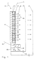
- a pulse generator of electrons comprises a cathode with field emission 1, to generate a flow of electrons 2 in direction of an anode 3.
- the field emission cathode 1 includes, so known, a conductive substrate 4, for example made of silicon, having an active face 5 on which micropoints 6-11 are arranged.
- the active face 5 is covered with an insulating layer 12, by example in silicon oxide, separating it from a grid 13 conductive.
- 6-11 microdots are housed in cavities respective 14-19 formed in the insulating layer 12 and communicating towards the anode 3 through openings corresponding provided in grid 13. The tips of 6-11 microtips come flush with the grid surface 13.
- the dimension of the cavities 14-19, and therefore the dimension of the microtips 6-11, is of the order of a micron in height and in width.
- Micropoint arrays are generally produced, the density of which is of the order of 10,000 to 100,000 microtips per mm 2 .
- Positive gate polarization means 20 are connected between the substrate 4 and the grid 13, to ensure the positive polarization of the grid 13.
- the means of gate positive bias 20 include a generator permanent positive prepolarization voltage 21, delivering a permanent positive prepolarization voltage V21, in series with a positive pulse voltage generator 22 delivering a positive pulse component V22 of bias voltage.
- Figure 3 illustrates the prepolarization voltage permanent positive V21, in the form of a direct voltage VR, and the positive impulse component V22 of voltage polarization, in the form of amplitude rectangular pulses VI.
- the electric current I corresponding to the flux of electrons emitted by the cathode is zero as long as the voltage of VGK gate polarization is less than a VS emission threshold of the cathode.
- the voltage of VGK polarization of the grid with respect to the cathode produces a electron current I which increases exponentially as a function of voltage.
- the threshold voltage VS is generally of the order of 50 to 100 volts, depending on the constitution of the network cathode microtips.
- a value of quiescent voltage VR which, during the non-emission steps of electrons, remains only slightly below the voltage of active polarization VA of gate 13.
- the voltage of active bias VA of gate 13 as being the voltage of VGK polarization from which anode 3 receives a non-flux negligible of electrons coming from cathode 1.
- an emission voltage value VE which, during the steps emission of electrons, is higher than said voltage of active gate VA polarization 13.
- the threshold voltage Emission VS of the cathode 1 we choose as active bias voltage value VA the threshold voltage Emission VS of the cathode 1.
- the voltage value of VR rest can then be chosen slightly lower than the voltage emission threshold VS of cathode 1.
- the transparent repellant grid 23 is interposed in the electron flow between the cathode grid 13 and the anode 3, and is biased by a generator 24 slightly below the emission threshold voltage VS of the cathode 1.
- the gate transparent repellant 23 pushes back towards cathode 1 the fluxes of electrons 25 having insufficient energy during the stages of no emission of electrons, while it lets the flux pass of electrons 2 having sufficient energy imparted by the voltage of emission polarization VE during the emission steps of electrons.
- an active bias voltage can be chosen VA slightly higher than the emission threshold voltage VS of the cathode 1.
- An electron pulse generator according to the invention can advantageously be used as a source of electrons in a time-of-flight mass spectrometer.
Landscapes
- Engineering & Computer Science (AREA)
- Analytical Chemistry (AREA)
- Physics & Mathematics (AREA)
- Chemical & Material Sciences (AREA)
- General Physics & Mathematics (AREA)
- Computer Hardware Design (AREA)
- Plasma & Fusion (AREA)
- Theoretical Computer Science (AREA)
- Cold Cathode And The Manufacture (AREA)
- Electron Sources, Ion Sources (AREA)
- Analysing Materials By The Use Of Radiation (AREA)
- Other Investigation Or Analysis Of Materials By Electrical Means (AREA)
- Control Of Indicators Other Than Cathode Ray Tubes (AREA)
Abstract
Description
- une valeur de tension de repos qui, pendant les étapes de non émission d'électrons, reste seulement légèrement inférieure à la tension de polarisation active de grille à partir de laquelle l'anode reçoit un flux non négligeable d'électrons provenant de la cathode,
- une valeur de tension d'émission qui, pendant les étapes d'émission d'électrons, est supérieure à ladite tension de polarisation active de grille.
- la figure 1 est une vue schématique montrant un générateur impulsionnel d'électrons selon un mode de réalisation de la présente invention ;
- la figure 2 illustre les caractéristiques tension / courant d'une cathode à émission de champ ; et
- la figure 3 illustre la constitution de la tension de polarisation de grille, et le courant électrique correspondant au flux d'électrons qui en résulte.
Claims (7)
- Générateur impulsionnel d'électrons, comprenant une cathode à émission de champ (1) à micropointes émettrices d'électrons (6-11) associées à une grille (13) polarisée par des moyens de polarisation positive de grille (20), avec une anode (3) attirant les électrons émis par la cathode (1), caractérisé en ce que les moyens de polarisation positive de grille (20) génèrent une tension de polarisation de grille (VGK) ayant :une valeur de tension de repos (VR) qui, pendant les étapes de non émission d'électrons, reste seulement légèrement inférieure à la tension de polarisation active (VA) de grille (13) à partir de laquelle l'anode (3) reçoit un flux non négligeable d'électrons provenant de la cathode (1),une valeur de tension d'émission (VE) qui, pendant les étapes d'émission d'électrons, est supérieure à ladite tension de polarisation active (VA) de grille (13).
- Générateur selon la revendication 1, caractérisé en ce que ladite valeur de tension de repos (VR) est légèrement inférieure à la tension de seuil d'émission (VS) de la cathode (1).
- Générateur selon l'une des revendications 1 ou 2, caractérisé en ce qu'une grille répulsive transparente (23) est interposée entre la grille (13) de cathode et l'anode (3), polarisée légèrement au-dessous de la tension de seuil d'émission (VS) de la cathode (1), pour repousser vers la cathode (1) les flux d'électrons (25) ayant une énergie insuffisante pendant les étapes de non émission d'électrons, et pour laisser passer les flux d'électrons (2) ayant une énergie suffisante pendant les étapes d'émission d'électrons.
- Générateur selon l'une quelconque des revendications 1 à 3, caractérisé en ce que les moyens de polarisation positive de grille (20) génèrent une tension de polarisation de grille (VGK) comprenant une tension de prépolarisation positive permanente (V21) à laquelle est superposée une composante impulsionnelle positive (V22) de tension de polarisation.
- Générateur selon la revendication 4, caractérisé en ce que les moyens de polarisation positive de grille (20) comprennent un générateur de tension de prépolarisation positive permanente (21), délivrant ladite tension de prépolarisation positive permanente (V21), en série avec un générateur de tension impulsionnelle positive (22) délivrant ladite composante impulsionnelle positive (V22) de tension de polarisation.
- Générateur selon l'une des revendications 4 ou 5, caractérisé en ce que ladite composante impulsionnelle positive (V22) de tension de polarisation a une amplitude (VI) de quelques volts seulement.
- Spectromètre de masse à temps de vol, caractérisé en ce qu'il comprend un générateur impulsionnel d'électrons selon l'une quelconque des revendications 1 à 6.
Applications Claiming Priority (2)
| Application Number | Priority Date | Filing Date | Title |
|---|---|---|---|
| FR9905087 | 1999-04-22 | ||
| FR9905087A FR2792771B1 (fr) | 1999-04-22 | 1999-04-22 | Generateur impulsionnel d'electrons |
Publications (2)
| Publication Number | Publication Date |
|---|---|
| EP1052680A1 true EP1052680A1 (fr) | 2000-11-15 |
| EP1052680B1 EP1052680B1 (fr) | 2007-01-03 |
Family
ID=9544731
Family Applications (1)
| Application Number | Title | Priority Date | Filing Date |
|---|---|---|---|
| EP00400835A Expired - Lifetime EP1052680B1 (fr) | 1999-04-22 | 2000-03-27 | Générateur impulsionnel d'électrons |
Country Status (6)
| Country | Link |
|---|---|
| US (1) | US6388384B1 (fr) |
| EP (1) | EP1052680B1 (fr) |
| JP (1) | JP2000353486A (fr) |
| AT (1) | ATE350761T1 (fr) |
| DE (1) | DE60032666T2 (fr) |
| FR (1) | FR2792771B1 (fr) |
Families Citing this family (6)
| Publication number | Priority date | Publication date | Assignee | Title |
|---|---|---|---|---|
| KR100766958B1 (ko) * | 2001-04-12 | 2007-10-15 | 삼성에스디아이 주식회사 | 전계 방출 표시장치 |
| JP3907626B2 (ja) * | 2003-01-28 | 2007-04-18 | キヤノン株式会社 | 電子源の製造方法、画像表示装置の製造方法、電子放出素子の製造方法、画像表示装置、特性調整方法、及び画像表示装置の特性調整方法 |
| JP3826120B2 (ja) * | 2003-07-25 | 2006-09-27 | キヤノン株式会社 | 電子放出素子、電子源及び画像表示装置の製造方法 |
| WO2005045874A1 (fr) * | 2003-10-31 | 2005-05-19 | Saintech Pty Ltd | Systeme de commande de source d'ions |
| EP2068343B1 (fr) * | 2007-11-13 | 2011-08-31 | ICT Integrated Circuit Testing Gesellschaft für Halbleiterprüftechnik mbH | Source de particules chargées avec formation automatisée de pointes |
| GB2464926A (en) * | 2008-10-28 | 2010-05-05 | Ex Beams Ltd | Apparatus for generating an electron beam |
Citations (1)
| Publication number | Priority date | Publication date | Assignee | Title |
|---|---|---|---|---|
| FR2734076A1 (fr) * | 1995-04-03 | 1996-11-15 | Motorola Inc | Dispositif a emission de champ ayant une source de courant transitoire |
Family Cites Families (5)
| Publication number | Priority date | Publication date | Assignee | Title |
|---|---|---|---|---|
| US3668384A (en) * | 1969-04-01 | 1972-06-06 | Bendix Corp | Mass spectrometer |
| US4990766A (en) * | 1989-05-22 | 1991-02-05 | Murasa International | Solid state electron amplifier |
| US5920296A (en) * | 1995-02-01 | 1999-07-06 | Pixel International | Flat screen having individually dipole-protected microdots |
| FR2750785B1 (fr) * | 1996-07-02 | 1998-11-06 | Pixtech Sa | Procede de regeneration de micropointes d'un ecran plat de visualisation |
| US5780960A (en) * | 1996-12-18 | 1998-07-14 | Texas Instruments Incorporated | Micro-machined field emission microtips |
-
1999
- 1999-04-22 FR FR9905087A patent/FR2792771B1/fr not_active Expired - Fee Related
-
2000
- 2000-03-27 DE DE60032666T patent/DE60032666T2/de not_active Expired - Fee Related
- 2000-03-27 EP EP00400835A patent/EP1052680B1/fr not_active Expired - Lifetime
- 2000-03-27 AT AT00400835T patent/ATE350761T1/de not_active IP Right Cessation
- 2000-04-04 US US09/543,154 patent/US6388384B1/en not_active Expired - Fee Related
- 2000-04-07 JP JP2000106050A patent/JP2000353486A/ja active Pending
Patent Citations (1)
| Publication number | Priority date | Publication date | Assignee | Title |
|---|---|---|---|---|
| FR2734076A1 (fr) * | 1995-04-03 | 1996-11-15 | Motorola Inc | Dispositif a emission de champ ayant une source de courant transitoire |
Non-Patent Citations (2)
| Title |
|---|
| C.CURTIS ET AL.: "spacecraft mass spectrometer ion source employing field emission cathodes", REVIEW SCIENTIFIC INSTRUMENTS, vol. 57, no. 5, May 1986 (1986-05-01), pages 989 - 990, XP002123493 * |
| E.POLLARD ET AL.: "ELECTRON-IMPACT IONIZATION TIME-OF-FLIGHT MASS SPECTROMETER FOR MOLECULAR BEAMS", REVIEW OF SCIENTIFIC INSTRUMENTS, vol. 58, no. 1, January 1987 (1987-01-01), pages 32 - 37, XP002123494 * |
Also Published As
| Publication number | Publication date |
|---|---|
| EP1052680B1 (fr) | 2007-01-03 |
| US6388384B1 (en) | 2002-05-14 |
| JP2000353486A (ja) | 2000-12-19 |
| FR2792771B1 (fr) | 2001-07-27 |
| ATE350761T1 (de) | 2007-01-15 |
| DE60032666D1 (de) | 2007-02-15 |
| FR2792771A1 (fr) | 2000-10-27 |
| DE60032666T2 (de) | 2007-10-11 |
Similar Documents
| Publication | Publication Date | Title |
|---|---|---|
| EP0172089B1 (fr) | Dispositif de visualisation par cathodoluminescence excitée par émission de champ | |
| EP0645947B1 (fr) | Tube neutronique à confinement magnétique des électrons par aimants permanents et son procédé de fabrication | |
| EP2337094B1 (fr) | Source de photons résultants d'une recombinaison d'excitons localisés | |
| FR2734076A1 (fr) | Dispositif a emission de champ ayant une source de courant transitoire | |
| EP1052680B1 (fr) | Générateur impulsionnel d'électrons | |
| FR2516307A1 (fr) | Dispositif semiconducteur pour l'emission d'electrons et dispositif muni d'un tel dispositif semiconducteur | |
| JP2927908B2 (ja) | 発光素子 | |
| EP0454566B1 (fr) | Laser compact à semi-conducteur du type à pompage électronique | |
| EP1825490B1 (fr) | Cathode à émission de champ à commande optique | |
| WO2000070638A1 (fr) | Procede et dispositif pour extraire des electrons dans le vide et cathodes d'emission pour un tel dispositif | |
| FR2669145A1 (fr) | Canon a electrons module par commutation optoelectronique. | |
| FR2784515A1 (fr) | Laser a semiconducteur a spectre de gain accordable | |
| EP0351263B1 (fr) | Structure de source d'électrons et application aux tubes d'émission d'ondes électromagnétiques | |
| FR2769405A1 (fr) | Dispositif a emission de champ | |
| EP0274940A1 (fr) | Dispositif de multiplication de porteurs de charge par un phénomène d'avalanche, et son application aux photodétecteurs, aux photocathodes, et aux visionneurs infrarouges | |
| EP2747118B1 (fr) | Cathode pour dispositif de génération d'ondes électromagnétiques, comprenant des régions d'émission mobiles les unes par rapport aux autres | |
| WO2013014109A1 (fr) | Dispositif semi-conducteur d'emission d'electrons dans le vide | |
| EP2747117B1 (fr) | Dispositif de génération d'ondes hyperfréquences à double cathodes | |
| EP3857618A1 (fr) | Source lumineuse matricielle pour un vehicule automobile | |
| FR2752643A1 (fr) | Cathode froide a emission de champ electrique | |
| EP1500121A1 (fr) | Panneau de visualisation a plasma a excitation des decharges par rayonnement micro-onde | |
| EP1249028B1 (fr) | Cathode generatrice d'electrons et son procede de fabrication | |
| WO2008074825A1 (fr) | Structure de cathode pour ecran plat avec grille de refocalisation | |
| FR2854984A1 (fr) | Dispositif semi-conducteur d'emission d'electrons dans le vide | |
| CH603005A5 (en) | Cold electron emitter using stainless steel comb |
Legal Events
| Date | Code | Title | Description |
|---|---|---|---|
| PUAI | Public reference made under article 153(3) epc to a published international application that has entered the european phase |
Free format text: ORIGINAL CODE: 0009012 |
|
| AK | Designated contracting states |
Kind code of ref document: A1 Designated state(s): AT BE CH CY DE DK ES FI FR GB GR IE IT LI LU MC NL PT SE |
|
| AX | Request for extension of the european patent |
Free format text: AL;LT;LV;MK;RO;SI |
|
| 17P | Request for examination filed |
Effective date: 20010515 |
|
| AKX | Designation fees paid |
Free format text: AT BE CH CY DE DK ES FI FR GB GR IE IT LI LU MC NL PT SE |
|
| GRAP | Despatch of communication of intention to grant a patent |
Free format text: ORIGINAL CODE: EPIDOSNIGR1 |
|
| GRAS | Grant fee paid |
Free format text: ORIGINAL CODE: EPIDOSNIGR3 |
|
| GRAA | (expected) grant |
Free format text: ORIGINAL CODE: 0009210 |
|
| AK | Designated contracting states |
Kind code of ref document: B1 Designated state(s): AT BE CH CY DE DK ES FI FR GB GR IE IT LI LU MC NL PT SE |
|
| PG25 | Lapsed in a contracting state [announced via postgrant information from national office to epo] |
Ref country code: IE Free format text: LAPSE BECAUSE OF FAILURE TO SUBMIT A TRANSLATION OF THE DESCRIPTION OR TO PAY THE FEE WITHIN THE PRESCRIBED TIME-LIMIT Effective date: 20070103 Ref country code: DK Free format text: LAPSE BECAUSE OF FAILURE TO SUBMIT A TRANSLATION OF THE DESCRIPTION OR TO PAY THE FEE WITHIN THE PRESCRIBED TIME-LIMIT Effective date: 20070103 Ref country code: NL Free format text: LAPSE BECAUSE OF FAILURE TO SUBMIT A TRANSLATION OF THE DESCRIPTION OR TO PAY THE FEE WITHIN THE PRESCRIBED TIME-LIMIT Effective date: 20070103 Ref country code: FI Free format text: LAPSE BECAUSE OF FAILURE TO SUBMIT A TRANSLATION OF THE DESCRIPTION OR TO PAY THE FEE WITHIN THE PRESCRIBED TIME-LIMIT Effective date: 20070103 Ref country code: AT Free format text: LAPSE BECAUSE OF FAILURE TO SUBMIT A TRANSLATION OF THE DESCRIPTION OR TO PAY THE FEE WITHIN THE PRESCRIBED TIME-LIMIT Effective date: 20070103 |
|
| REG | Reference to a national code |
Ref country code: GB Ref legal event code: FG4D Free format text: NOT ENGLISH |
|
| REF | Corresponds to: |
Ref document number: 60032666 Country of ref document: DE Date of ref document: 20070215 Kind code of ref document: P |
|
| PG25 | Lapsed in a contracting state [announced via postgrant information from national office to epo] |
Ref country code: SE Free format text: LAPSE BECAUSE OF FAILURE TO SUBMIT A TRANSLATION OF THE DESCRIPTION OR TO PAY THE FEE WITHIN THE PRESCRIBED TIME-LIMIT Effective date: 20070403 |
|
| RAP2 | Party data changed (patent owner data changed or rights of a patent transferred) |
Owner name: ALCATEL LUCENT |
|
| GBT | Gb: translation of ep patent filed (gb section 77(6)(a)/1977) |
Effective date: 20070315 |
|
| PG25 | Lapsed in a contracting state [announced via postgrant information from national office to epo] |
Ref country code: ES Free format text: LAPSE BECAUSE OF FAILURE TO SUBMIT A TRANSLATION OF THE DESCRIPTION OR TO PAY THE FEE WITHIN THE PRESCRIBED TIME-LIMIT Effective date: 20070414 |
|
| NLT2 | Nl: modifications (of names), taken from the european patent patent bulletin |
Owner name: ALCATEL LUCENT Effective date: 20070404 |
|
| PG25 | Lapsed in a contracting state [announced via postgrant information from national office to epo] |
Ref country code: PT Free format text: LAPSE BECAUSE OF FAILURE TO SUBMIT A TRANSLATION OF THE DESCRIPTION OR TO PAY THE FEE WITHIN THE PRESCRIBED TIME-LIMIT Effective date: 20070604 |
|
| NLV1 | Nl: lapsed or annulled due to failure to fulfill the requirements of art. 29p and 29m of the patents act | ||
| REG | Reference to a national code |
Ref country code: FR Ref legal event code: CD |
|
| REG | Reference to a national code |
Ref country code: IE Ref legal event code: FD4D |
|
| PLBE | No opposition filed within time limit |
Free format text: ORIGINAL CODE: 0009261 |
|
| STAA | Information on the status of an ep patent application or granted ep patent |
Free format text: STATUS: NO OPPOSITION FILED WITHIN TIME LIMIT |
|
| REG | Reference to a national code |
Ref country code: CH Ref legal event code: PL |
|
| 26N | No opposition filed |
Effective date: 20071005 |
|
| BERE | Be: lapsed |
Owner name: ALCATEL Effective date: 20070331 |
|
| PG25 | Lapsed in a contracting state [announced via postgrant information from national office to epo] |
Ref country code: BE Free format text: LAPSE BECAUSE OF NON-PAYMENT OF DUE FEES Effective date: 20070331 |
|
| PG25 | Lapsed in a contracting state [announced via postgrant information from national office to epo] |
Ref country code: MC Free format text: LAPSE BECAUSE OF NON-PAYMENT OF DUE FEES Effective date: 20070331 |
|
| PG25 | Lapsed in a contracting state [announced via postgrant information from national office to epo] |
Ref country code: LI Free format text: LAPSE BECAUSE OF NON-PAYMENT OF DUE FEES Effective date: 20070331 Ref country code: CH Free format text: LAPSE BECAUSE OF NON-PAYMENT OF DUE FEES Effective date: 20070331 |
|
| PG25 | Lapsed in a contracting state [announced via postgrant information from national office to epo] |
Ref country code: GR Free format text: LAPSE BECAUSE OF FAILURE TO SUBMIT A TRANSLATION OF THE DESCRIPTION OR TO PAY THE FEE WITHIN THE PRESCRIBED TIME-LIMIT Effective date: 20070404 Ref country code: IT Free format text: LAPSE BECAUSE OF NON-PAYMENT OF DUE FEES Effective date: 20070327 |
|
| PGFP | Annual fee paid to national office [announced via postgrant information from national office to epo] |
Ref country code: GB Payment date: 20080320 Year of fee payment: 9 |
|
| PGFP | Annual fee paid to national office [announced via postgrant information from national office to epo] |
Ref country code: DE Payment date: 20080321 Year of fee payment: 9 Ref country code: FR Payment date: 20080314 Year of fee payment: 9 |
|
| PG25 | Lapsed in a contracting state [announced via postgrant information from national office to epo] |
Ref country code: CY Free format text: LAPSE BECAUSE OF FAILURE TO SUBMIT A TRANSLATION OF THE DESCRIPTION OR TO PAY THE FEE WITHIN THE PRESCRIBED TIME-LIMIT Effective date: 20070103 |
|
| PG25 | Lapsed in a contracting state [announced via postgrant information from national office to epo] |
Ref country code: LU Free format text: LAPSE BECAUSE OF NON-PAYMENT OF DUE FEES Effective date: 20070327 |
|
| GBPC | Gb: european patent ceased through non-payment of renewal fee |
Effective date: 20090327 |
|
| REG | Reference to a national code |
Ref country code: FR Ref legal event code: ST Effective date: 20091130 |
|
| PG25 | Lapsed in a contracting state [announced via postgrant information from national office to epo] |
Ref country code: DE Free format text: LAPSE BECAUSE OF NON-PAYMENT OF DUE FEES Effective date: 20091001 |
|
| PG25 | Lapsed in a contracting state [announced via postgrant information from national office to epo] |
Ref country code: GB Free format text: LAPSE BECAUSE OF NON-PAYMENT OF DUE FEES Effective date: 20090327 Ref country code: FR Free format text: LAPSE BECAUSE OF NON-PAYMENT OF DUE FEES Effective date: 20091123 |
|
| REG | Reference to a national code |
Ref country code: FR Ref legal event code: CA Effective date: 20150521 |
|
| REG | Reference to a national code |
Ref country code: FR Ref legal event code: CA Effective date: 20150521 |