EP1052677A2 - Electron emitters for lithography tools - Google Patents
Electron emitters for lithography tools Download PDFInfo
- Publication number
- EP1052677A2 EP1052677A2 EP00303780A EP00303780A EP1052677A2 EP 1052677 A2 EP1052677 A2 EP 1052677A2 EP 00303780 A EP00303780 A EP 00303780A EP 00303780 A EP00303780 A EP 00303780A EP 1052677 A2 EP1052677 A2 EP 1052677A2
- Authority
- EP
- European Patent Office
- Prior art keywords
- electron
- electron beam
- mesh grid
- emitter
- gun
- Prior art date
- Legal status (The legal status is an assumption and is not a legal conclusion. Google has not performed a legal analysis and makes no representation as to the accuracy of the status listed.)
- Granted
Links
Images



Classifications
-
- H—ELECTRICITY
- H01—ELECTRIC ELEMENTS
- H01J—ELECTRIC DISCHARGE TUBES OR DISCHARGE LAMPS
- H01J37/00—Discharge tubes with provision for introducing objects or material to be exposed to the discharge, e.g. for the purpose of examination or processing thereof
- H01J37/02—Details
- H01J37/04—Arrangements of electrodes and associated parts for generating or controlling the discharge, e.g. electron-optical arrangement or ion-optical arrangement
- H01J37/06—Electron sources; Electron guns
- H01J37/065—Construction of guns or parts thereof
-
- H—ELECTRICITY
- H10—SEMICONDUCTOR DEVICES; ELECTRIC SOLID-STATE DEVICES NOT OTHERWISE PROVIDED FOR
- H10P—GENERIC PROCESSES OR APPARATUS FOR THE MANUFACTURE OR TREATMENT OF DEVICES COVERED BY CLASS H10
- H10P76/00—Manufacture or treatment of masks on semiconductor bodies, e.g. by lithography or photolithography
-
- H—ELECTRICITY
- H01—ELECTRIC ELEMENTS
- H01J—ELECTRIC DISCHARGE TUBES OR DISCHARGE LAMPS
- H01J2237/00—Discharge tubes exposing object to beam, e.g. for analysis treatment, etching, imaging
- H01J2237/30—Electron or ion beam tubes for processing objects
- H01J2237/317—Processing objects on a microscale
- H01J2237/3175—Lithography
-
- Y—GENERAL TAGGING OF NEW TECHNOLOGICAL DEVELOPMENTS; GENERAL TAGGING OF CROSS-SECTIONAL TECHNOLOGIES SPANNING OVER SEVERAL SECTIONS OF THE IPC; TECHNICAL SUBJECTS COVERED BY FORMER USPC CROSS-REFERENCE ART COLLECTIONS [XRACs] AND DIGESTS
- Y10—TECHNICAL SUBJECTS COVERED BY FORMER USPC
- Y10S—TECHNICAL SUBJECTS COVERED BY FORMER USPC CROSS-REFERENCE ART COLLECTIONS [XRACs] AND DIGESTS
- Y10S430/00—Radiation imagery chemistry: process, composition, or product thereof
- Y10S430/143—Electron beam
Definitions
- This invention relates to electron beam lithography apparatus used for the manufacture of semiconductor integrated circuits.
- Electron beam exposure tools have been used for lithography in semiconductor processing for more than two decades.
- the first e-beam exposure tools were based on the flying spot concept of a highly focused beam, raster scanned over the object plane.
- the electron beam is modulated as it scans so that the beam itself generates the lithographic pattern.
- These tools have been widely used for high precision tasks, such as lithographic mask making, but the raster scan mode is found to be too slow to enable the high throughput required in semiconductor wafer processing.
- the electron source in this equipment is similar to that used in electron microscopes, i.e. a high brightness source focused to a small spot beam.
- the requirements for the electron beam source in SCALPEL exposure tools differ significantly from those of a conventional focused beam exposure tool, or a conventional TEM or SEM. While high resolution imaging is still a primary goal, this must be achieved at relatively high (10-100 ⁇ A) gun currents in order to realize economic wafer throughput.
- the axial brightness required is relatively low, e.g. 10 2 to 10 4 Acm -2 sr -1 , as compared with a value of 10 6 to 10 9 Acm -2 sr -1 for a typical focused beam source.
- the beam flux over the larger area must be highly uniform to obtain the required lithographic dose latitude and CD control.
- the beam shaping element is a mesh grid that is installed over the opening in the Wehnelt gun.
- the mesh grid is an equipotential screen with each aperture in the screen acting as a separate Wehnelt emitter with its own funnel-shaped electrical field. The result is a highly uniform wide area electron beam that is ideally suited for SCALPEL tools.
- the optical analog of the proposed gridded Wehnelt is a fly's eye lens, or scatter plates or diffusers, which transform non-uniform light beams into uniform beams in optical illumination systems.
- a conventional Wehnelt electron gun assembly is shown with base 11, cathode support arms 12, cathode filament 13, Wehnelt electrode comprised of Wehnelt support arms 15 and conventional Wehnelt aperture 16.
- the base 11 may be ceramic
- the support members 12 may be tantalum, steel, or molybdenum.
- the filament 13 may be tungsten wire
- the material forming the Wehnelt aperture may be steel or tantalum
- the electron emitter 14 is, e.g., a tantalum disk.
- the effective area of the electron emitter is typically in the range of 0.5-3 mm 2 .
- the electron emitter is preferably a disk with a diameter in the range 0.5-2.0 mm.
- the anode is shown schematically at 17, and the electron beam at 18.
- the beam control apparatus which is conventional and well known in the art, is not shown. It will be appreciated by those skilled in the art that the dimensions in the figures are not necessarily to scale.
- An important feature of the electron source for SCALPEL exposure tools is relatively low electron beam brightness, as mentioned earlier. For most effective exposures, it is preferred that beam brightness be limited to a value less than 10 4 Acm -2 sr -1 . This is in contrast with conventional scanning electron beam exposure tools which are typically optimized for maximum brightness. See e.g. U. S. Patent No. 4,588,928 issued May 13, 1986 to Liu et al.
- the improved electron gun according to the invention is shown in Fig. 2.
- the opening for the Wehnelt is provided with mesh grid 23, disposed in the path of the electron emission 25.
- the mesh grid 23 is at a potential equal to the Wehnelt electrode and functions as a secondary emitter with multiple sources.
- the electron emission pattern from a standard round bore Wehnelt gun i.e. the gun of Fig. 1, is shown in Fig. 3.
- the relatively non-uniform, bell curve shaped output from the Wehnelt is evident.
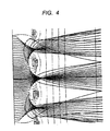
- the electron emission pattern from the mesh grid equipped Wehnelt gun of the invention i.e. the gun of Fig. 2, is shown in Fig. 4.
- the multiple emission patterns can be seen, which serve to spatially distribute the electron flux across a wide aperture and ensure a flat averaged electrical field over the cathode surface.
- the individual electron beams overlap and the integrated electron flux is highly uniform.
- the screen element that forms the mesh grid can have a variety of configurations. The simplest is a conventional woven screen with square apertures. However, the screen may have triangular shaped apertures, hexagonal close packed apertures, or even circular apertures. It can be woven or non-woven. Techniques for forming suitable screens from a continuous layer may occur to those skilled in the art. For example, multiple openings in a continuous metal sheet or foil can be produced by techniques such as laser drilling. Fine meshes can also be formed by electroforming techniques.
- the mesh grid should be electrically conducting but the material of the mesh is otherwise is relatively inconsequential. Tantalum, tungsten, molybdenum, titanium, or even steel are suitable materials.
- the mesh grid preferably has a transparency in the range 40-90 %, with transparency defined as the two dimensional void space divided by the overall mesh grid area.
- the spacing between the electron emitter surface and the mesh grid is typically in the range 0.1 to 1.0 mm.
- the mesh grid has bars “b” of approximately 50 ⁇ m, and square cells with “C” approximately 200 ⁇ m.
- This mesh grid has a transparency of approximately 65%.
- Mesh grid structures that were found suitable are represented by the examples in the following table. Cell dimension "C”, ⁇ m Bar width "b”, ⁇ m Grid #100 200 50 Grid #200 88 37 Grid #300 54 31
- the cell dimension "C” is the width of the opening in a mesh with a square opening.
- the dimension "C” is approximately the square root of the area of the opening. It is preferred that the openings be approximately symmetrical, i.e. square or round.
- the electron gun of the invention is most advantageously utilized as the electron source in a SCALPEL electron beam lithography machine.
- Fabrication of semiconductor devices on semiconductor wafers in current industry practice contemplates the exposure of polymer resist materials with fine line patterns of actinic radiation, in this case, electron beam radiation. This is achieved in conventional practice by directing the actinic radiation through a lithographic mask and onto a resist coated substrate.
- the mask may be positioned close to the substrate for proximity printing or may be placed away from the substrate and the image of the mask projected onto the substrate for projection printing.
- SCALPEL lithography tools are characterized by high contrast image patterns at very small linewidths, i.e 0.1 ⁇ m or less. They produce high resolution images with wide process latitude, coupled with the high throughput of optical projection systems.
- the high throughput is made possible by using a flood beam of electrons to expose a relatively large area of the wafer. Electron beam optics, comprising standard magnetic field beam steering and focusing, are used to image the flood beam onto the lithographic mask, and thereafter, onto the substrate, i.e. the resist coated wafer.
- the lithographic mask is composed of regions of high electron scattering and regions of low electron scattering, which regions define the features desired in the mask pattern. Details of suitable mask structures can be found in U.S. Patents Nos. 5,079,112 issued Jan. 7, 1992, and 5,258,246 issued Nov. 2, 1993, both to Berger et al.
- the back focal plane filter functions by blocking the highly scattered electrons while passing the weakly scattered electrons, thus forming the image pattern on the substrate.
- the blocking filter thus absorbs the unwanted radiation in the image. This is in contrast to conventional lithography tools in which the unwanted radiation in the image is absorbed by the mask itself, contributing to heating and distortion of the mask, and to reduced mask lifetime.
- Lithographic mask 52 is illuminated with a uniform flood beam 51 of 100 keV electrons produced by the electron gun of Fig. 2.
- the membrane mask 52 comprises regions 53 of high scattering material and regions 54 of low scattering material.
- the weakly scattered portions of the beam, i.e. rays 51a, are focused by magnetic lens 55 through the aperture 57 of the back focal plane blocking filter 56.
- the back focal plane filter 56 may be a silicon wafer or other material suitable for blocking electrons.
- the highly scattered portions of the electron beam, represented here by rays 51b and 51c, are blocked by the back focal plane filter 56.
- Regions 60 replicate the features 54 of the lithographic mask 52, i.e. the regions to be exposed, and regions 61 replicate the features 53 of the lithographic mask, i.e. the regions that are not to be exposed. These regions are interchangeable, as is well known in the art, to produce either negative or positive resist patterns.
- the vitalizing feature of the SCALPEL tool is the positioning of a blocking filter at or near the back focal plane of the electron beam image. Further details of SCALPEL systems can be found in U.S. Patents Nos. 5,079,112 issued Jan. 7, 1992, and 5,258,246 issued Nov. 2, 1993, both to Berger et al. These patents are incorporated herein by reference for such details that may be found useful for the practice of the invention.
- wehnelt emitter is intended to define a solid metal body with an approximately flat emitting surface, said flat emitting surface being symmetrical, i.e. having the shape of a circle or regular polygon.
- substrate is used herein to define the object plane of the electron beam exposure system whether or not there is a semiconductor workpiece present on the substrate.
- electron optics plane may be used to describe an x-y plane in space in the electron beam exposure system between the electron emitting surface of the electron gun and the surface onto which the electron beam image is focused, i.e. the object plane where the semiconductor wafer is situated.
- the grid bias required for far field beam shaping and for regulating exposure dose in the modified Wehnelt gun of the invention is not.
- the cut-off bias in conventional Wehnelt guns is typically 400 V or more. Because of the presence of the mesh grid in the modified Wehnelt gun of the invention, cut-off for the grid bias is less than 100 V, and in most structures, e.g. the embodiment described above, less than 50 V. This voltage can be applied directly to the Wehnelt electrode and can be switched or modulated using semiconductor drive circuits, which sharply reduces the cost of the apparatus and the response time of the beam control system.
- the wobble can be produced by a low frequency, i.e. 1-10 kHz, beam drive signal that is superimposed on the Wehnelt grid bias. This wobble changes the beam pattern at the frequency of the wobble so that any peaks or hot spots in the electron beam front are moved periodically and the integrated flux over time is more spatially equalized.
Landscapes
- Chemical & Material Sciences (AREA)
- Analytical Chemistry (AREA)
- Electron Beam Exposure (AREA)
- Electron Sources, Ion Sources (AREA)
Abstract
Description
| Cell dimension "C", µm | Bar width "b", µm | |
| Grid #100 | 200 | 50 |
| Grid #200 | 88 | 37 |
| Grid #300 | 54 | 31 |
D : b >= 4 ; C : t > = 1.5
where D is the cathode-to-grid distance.
Claims (10)
- Method for the manufacture of semiconductor integrated circuits comprising at least one lithographic step in which a patterned electron beam is projected onto the surface of a resist coated semiconductor wafer using a lens system, the method comprising the steps of:(a) projecting a beam of electrons onto said resist coated semiconductor wafer sequentially through:the method characterized in that said electron beam is produced by an electron gun and said electron gun is operated by(i) a lithographic mask, and(ii) a back focal plane filter, said back focal plane filter being essentially opaque to electrons in said electron beam,(b) establishing a bias between an electron emitter as cathode and an anode spaced from said electron emitter, said electron gun having a conductive mesh grid between said electron emitter and said anode so that said electron beam flows from said electron emitter, through said conductive mesh grid, to said anode.
- The method of claim 1 wherein said electron beam has a brightness of less than 104 Acm-2sr-1.
- The method of claim 1 wherein said mesh grid has a transparency between 40-90%.
- An electron beam exposure system comprising:(a) an electron beam emitter,(b) a conductive mesh grid,(c) a positive anode.(d) a lithographic mask,(e) a back focal plane filter,(f) a substrate,(g) means including biasing means for producing an electron beam from said electron beam emitter, and(h) means for directing at least portions of said electron beam sequentially through said conductive mesh grid, through said positive anode, through said lithographic mask, through said back focal plane filter, and onto said substrate.
- The system of claim 4 wherein said mesh grid has a transparency between 40-90%.
- The system of claim 5 wherein the mesh of said mesh grid is an electroformed grid.
- The system of claim 4 wherein said mesh grid is spaced from said electron emitter by a distance in the range 0.1 to 1.0 mm.
- The system of claim 4 wherein the electron emitter comprises a tantalum disk.
- The system of claim 4 further including bias means for biasing said electron emitter at a voltage of less than 100 V.
- The system of claim 9 wherein said bias means includes means for biasing said electron emitter with an alternating voltage.
Applications Claiming Priority (2)
| Application Number | Priority Date | Filing Date | Title |
|---|---|---|---|
| US09/306,287 US6232040B1 (en) | 1999-05-06 | 1999-05-06 | Method of electron beam exposure utilizing emitter with conductive mesh grid |
| US306287 | 2002-11-27 |
Publications (3)
| Publication Number | Publication Date |
|---|---|
| EP1052677A2 true EP1052677A2 (en) | 2000-11-15 |
| EP1052677A3 EP1052677A3 (en) | 2006-06-07 |
| EP1052677B1 EP1052677B1 (en) | 2008-07-23 |
Family
ID=23184628
Family Applications (1)
| Application Number | Title | Priority Date | Filing Date |
|---|---|---|---|
| EP00303780A Expired - Lifetime EP1052677B1 (en) | 1999-05-06 | 2000-05-05 | Electron emitters for lithography tools |
Country Status (6)
| Country | Link |
|---|---|
| US (2) | US6232040B1 (en) |
| EP (1) | EP1052677B1 (en) |
| JP (1) | JP3492977B2 (en) |
| KR (1) | KR100634727B1 (en) |
| DE (1) | DE60039551D1 (en) |
| TW (1) | TW591327B (en) |
Cited By (1)
| Publication number | Priority date | Publication date | Assignee | Title |
|---|---|---|---|---|
| EP1091386A2 (en) | 1999-10-07 | 2001-04-11 | Lucent Technologies Inc. | Illumination system for electron beam lithography tool |
Families Citing this family (18)
| Publication number | Priority date | Publication date | Assignee | Title |
|---|---|---|---|---|
| JP2000182550A (en) * | 1998-12-18 | 2000-06-30 | Canon Inc | Electron gun and illumination device or electron beam exposure device using the electron gun |
| US6232040B1 (en) * | 1999-05-06 | 2001-05-15 | Agere Systems, Inc. | Method of electron beam exposure utilizing emitter with conductive mesh grid |
| DE60033767T2 (en) * | 1999-06-22 | 2007-11-15 | Fei Co., Hillsboro | CORPUSCULAR OPTICAL DEVICE WITH A PARTICLE SOURCE SWITCHABLE BETWEEN HIGH BRIGHTNESS AND LARGE RADIATION CURRENT |
| US6576529B1 (en) * | 1999-12-07 | 2003-06-10 | Agere Systems Inc. | Method of forming an alignment feature in or on a multilayered semiconductor structure |
| JP2002163005A (en) * | 2000-11-29 | 2002-06-07 | Nikon Corp | Control system design method, control system, control system adjustment method, and exposure method |
| WO2002091421A1 (en) * | 2001-05-01 | 2002-11-14 | Nikon Corporation | Electron beam apparatus and device manufacturing method using the electron beam apparatus |
| AU2002366886A1 (en) * | 2001-12-20 | 2003-07-09 | Koninklijke Philips Electronics N.V. | Cathode ray tube and electron gun |
| US6822241B2 (en) | 2002-10-03 | 2004-11-23 | Hewlett-Packard Development Company, L.P. | Emitter device with focusing columns |
| US7057353B2 (en) * | 2003-01-13 | 2006-06-06 | Hewlett-Packard Development Company, L.P. | Electronic device with wide lens for small emission spot size |
| JP2005088801A (en) | 2003-09-18 | 2005-04-07 | Denso Corp | Information processing system |
| US7454221B1 (en) * | 2005-07-12 | 2008-11-18 | Hewlett-Packard Development Company, L.P. | Electron tube amplification |
| JP5241195B2 (en) * | 2006-10-30 | 2013-07-17 | アイエムエス ナノファブリカツィオン アーゲー | Charged particle exposure system |
| DE102007042108B4 (en) * | 2007-09-05 | 2010-02-11 | Siemens Ag | Electron source with associated measured value acquisition |
| CN101452797B (en) | 2007-12-05 | 2011-11-09 | 清华大学 | Field emission type electronic source and manufacturing method thereof |
| US8340250B2 (en) * | 2009-09-04 | 2012-12-25 | General Electric Company | System and method for generating X-rays |
| US10192708B2 (en) * | 2015-11-20 | 2019-01-29 | Oregon Physics, Llc | Electron emitter source |
| GB2619965A (en) * | 2022-06-24 | 2023-12-27 | Aquasium Tech Limited | Electron beam emitting assembly |
| CN119172916B (en) * | 2024-11-25 | 2025-03-25 | 上海福照人间技术有限公司 | Electron beam control device and electron accelerator |
Family Cites Families (11)
| Publication number | Priority date | Publication date | Assignee | Title |
|---|---|---|---|---|
| US3852633A (en) * | 1972-12-13 | 1974-12-03 | Varian Associates | Gridded electron gun |
| US3833482A (en) * | 1973-03-26 | 1974-09-03 | Buckbee Mears Co | Matrix for forming mesh |
| US4588928A (en) * | 1983-06-15 | 1986-05-13 | At&T Bell Laboratories | Electron emission system |
| JPS6074336A (en) * | 1983-09-30 | 1985-04-26 | Nec Corp | Rectangular electron beam generator |
| US4767964A (en) * | 1987-02-04 | 1988-08-30 | Tektronix, Inc. | Improved mesh for CRT scan expansion lens and lens fabricated therefrom |
| US5258246A (en) * | 1989-08-07 | 1993-11-02 | At&T Bell Laboratories | Device manufacture involving lithographic processing |
| US5079112A (en) * | 1989-08-07 | 1992-01-07 | At&T Bell Laboratories | Device manufacture involving lithographic processing |
| US5759078A (en) * | 1995-05-30 | 1998-06-02 | Texas Instruments Incorporated | Field emission device with close-packed microtip array |
| JPH10223166A (en) * | 1997-01-31 | 1998-08-21 | Nikon Corp | Electron gun |
| JPH10261380A (en) * | 1997-03-19 | 1998-09-29 | Nikon Corp | Electron optics |
| US6232040B1 (en) * | 1999-05-06 | 2001-05-15 | Agere Systems, Inc. | Method of electron beam exposure utilizing emitter with conductive mesh grid |
-
1999
- 1999-05-06 US US09/306,287 patent/US6232040B1/en not_active Expired - Lifetime
-
2000
- 2000-05-04 KR KR1020000023964A patent/KR100634727B1/en not_active Expired - Fee Related
- 2000-05-05 DE DE60039551T patent/DE60039551D1/en not_active Expired - Lifetime
- 2000-05-05 EP EP00303780A patent/EP1052677B1/en not_active Expired - Lifetime
- 2000-05-08 JP JP2000135070A patent/JP3492977B2/en not_active Expired - Fee Related
- 2000-07-15 TW TW089108620A patent/TW591327B/en not_active IP Right Cessation
-
2001
- 2001-03-27 US US09/818,799 patent/US6400090B2/en not_active Expired - Lifetime
Cited By (2)
| Publication number | Priority date | Publication date | Assignee | Title |
|---|---|---|---|---|
| EP1091386A2 (en) | 1999-10-07 | 2001-04-11 | Lucent Technologies Inc. | Illumination system for electron beam lithography tool |
| EP1091386A3 (en) * | 1999-10-07 | 2006-03-01 | Lucent Technologies Inc. | Illumination system for electron beam lithography tool |
Also Published As
| Publication number | Publication date |
|---|---|
| EP1052677A3 (en) | 2006-06-07 |
| US20010022347A1 (en) | 2001-09-20 |
| JP2001023897A (en) | 2001-01-26 |
| EP1052677B1 (en) | 2008-07-23 |
| US6232040B1 (en) | 2001-05-15 |
| US6400090B2 (en) | 2002-06-04 |
| TW591327B (en) | 2004-06-11 |
| KR100634727B1 (en) | 2006-10-17 |
| JP3492977B2 (en) | 2004-02-03 |
| DE60039551D1 (en) | 2008-09-04 |
| KR20010014869A (en) | 2001-02-26 |
Similar Documents
| Publication | Publication Date | Title |
|---|---|---|
| US6400090B2 (en) | Electron emitters for lithography tools | |
| US6333508B1 (en) | Illumination system for electron beam lithography tool | |
| US6335783B1 (en) | Lithography system | |
| JP2002541623A (en) | Electrostatic Focused Addressable Field Emission Array Chip (AFEA's) for High Speed Massively Parallel Maskless Digital Electron Beam Direct Writing Lithography and Scanning Electron Microscopy | |
| KR100572251B1 (en) | Apparatus and method for suppressing space charge induced aberration in charged particle projection lithography systems | |
| US6218676B1 (en) | Charged-particle-beam image-transfer apparatus exhibiting reduced space-charge effects and device fabrication methods using the same | |
| KR100365880B1 (en) | Shaped shadow projection for an electron beam column | |
| US6091187A (en) | High emittance electron source having high illumination uniformity | |
| KR100757215B1 (en) | Illumination system for electron beam lithography tool | |
| JPH01159955A (en) | Electronic image projector | |
| EP1052678B1 (en) | Lithography tool with electron gun | |
| JP2002289517A (en) | Electron beam proximity exposure apparatus and method | |
| JPH1186766A (en) | Electron beam transfer exposure equipment | |
| JP2004193157A (en) | Electron beam illumination optical system and electron beam exposure apparatus | |
| JP2000058448A (en) | Electron beam transfer apparatus and semiconductor device manufacturing method |
Legal Events
| Date | Code | Title | Description |
|---|---|---|---|
| PUAI | Public reference made under article 153(3) epc to a published international application that has entered the european phase |
Free format text: ORIGINAL CODE: 0009012 |
|
| AK | Designated contracting states |
Kind code of ref document: A2 Designated state(s): AT BE CH CY DE DK ES FI FR GB GR IE IT LI LU MC NL PT SE |
|
| AX | Request for extension of the european patent |
Free format text: AL;LT;LV;MK;RO;SI |
|
| PUAL | Search report despatched |
Free format text: ORIGINAL CODE: 0009013 |
|
| AK | Designated contracting states |
Kind code of ref document: A3 Designated state(s): AT BE CH CY DE DK ES FI FR GB GR IE IT LI LU MC NL PT SE |
|
| AX | Request for extension of the european patent |
Extension state: AL LT LV MK RO SI |
|
| 17P | Request for examination filed |
Effective date: 20061205 |
|
| AKX | Designation fees paid |
Designated state(s): DE FR GB |
|
| 17Q | First examination report despatched |
Effective date: 20070130 |
|
| GRAP | Despatch of communication of intention to grant a patent |
Free format text: ORIGINAL CODE: EPIDOSNIGR1 |
|
| GRAS | Grant fee paid |
Free format text: ORIGINAL CODE: EPIDOSNIGR3 |
|
| GRAA | (expected) grant |
Free format text: ORIGINAL CODE: 0009210 |
|
| AK | Designated contracting states |
Kind code of ref document: B1 Designated state(s): DE FR GB |
|
| REG | Reference to a national code |
Ref country code: GB Ref legal event code: FG4D |
|
| REF | Corresponds to: |
Ref document number: 60039551 Country of ref document: DE Date of ref document: 20080904 Kind code of ref document: P |
|
| PLBE | No opposition filed within time limit |
Free format text: ORIGINAL CODE: 0009261 |
|
| STAA | Information on the status of an ep patent application or granted ep patent |
Free format text: STATUS: NO OPPOSITION FILED WITHIN TIME LIMIT |
|
| 26N | No opposition filed |
Effective date: 20090424 |
|
| PGFP | Annual fee paid to national office [announced via postgrant information from national office to epo] |
Ref country code: FR Payment date: 20140509 Year of fee payment: 15 |
|
| REG | Reference to a national code |
Ref country code: DE Ref legal event code: R082 Ref document number: 60039551 Country of ref document: DE Representative=s name: DILG HAEUSLER SCHINDELMANN PATENTANWALTSGESELL, DE |
|
| PGFP | Annual fee paid to national office [announced via postgrant information from national office to epo] |
Ref country code: GB Payment date: 20150424 Year of fee payment: 16 |
|
| REG | Reference to a national code |
Ref country code: FR Ref legal event code: ST Effective date: 20160129 |
|
| PG25 | Lapsed in a contracting state [announced via postgrant information from national office to epo] |
Ref country code: FR Free format text: LAPSE BECAUSE OF NON-PAYMENT OF DUE FEES Effective date: 20150601 |
|
| GBPC | Gb: european patent ceased through non-payment of renewal fee |
Effective date: 20160505 |
|
| PG25 | Lapsed in a contracting state [announced via postgrant information from national office to epo] |
Ref country code: GB Free format text: LAPSE BECAUSE OF NON-PAYMENT OF DUE FEES Effective date: 20160505 |
|
| PGFP | Annual fee paid to national office [announced via postgrant information from national office to epo] |
Ref country code: DE Payment date: 20170420 Year of fee payment: 18 |
|
| REG | Reference to a national code |
Ref country code: DE Ref legal event code: R082 Ref document number: 60039551 Country of ref document: DE Representative=s name: DILG HAEUSLER SCHINDELMANN PATENTANWALTSGESELL, DE Ref country code: DE Ref legal event code: R081 Ref document number: 60039551 Country of ref document: DE Owner name: AVAGO TECHNOLOGIES GENERAL IP (SINGAPORE) PTE., SG Free format text: FORMER OWNER: LUCENT TECHNOLOGIES INC., MURRAY HILL, N.J., US |
|
| REG | Reference to a national code |
Ref country code: DE Ref legal event code: R119 Ref document number: 60039551 Country of ref document: DE |
|
| PG25 | Lapsed in a contracting state [announced via postgrant information from national office to epo] |
Ref country code: DE Free format text: LAPSE BECAUSE OF NON-PAYMENT OF DUE FEES Effective date: 20181201 |