EP1050907A2 - Photosensor structure - Google Patents
Photosensor structure Download PDFInfo
- Publication number
- EP1050907A2 EP1050907A2 EP00303670A EP00303670A EP1050907A2 EP 1050907 A2 EP1050907 A2 EP 1050907A2 EP 00303670 A EP00303670 A EP 00303670A EP 00303670 A EP00303670 A EP 00303670A EP 1050907 A2 EP1050907 A2 EP 1050907A2
- Authority
- EP
- European Patent Office
- Prior art keywords
- layer
- photosensor
- transparent conductive
- conductive layer
- substrate
- Prior art date
- Legal status (The legal status is an assumption and is not a legal conclusion. Google has not performed a legal analysis and makes no representation as to the accuracy of the status listed.)
- Withdrawn
Links
- 239000000758 substrate Substances 0.000 claims abstract description 69
- 239000004020 conductor Substances 0.000 description 104
- 239000007789 gas Substances 0.000 description 81
- 238000000034 method Methods 0.000 description 56
- 238000000151 deposition Methods 0.000 description 43
- XUIMIQQOPSSXEZ-UHFFFAOYSA-N Silicon Chemical compound [Si] XUIMIQQOPSSXEZ-UHFFFAOYSA-N 0.000 description 32
- 229910052710 silicon Inorganic materials 0.000 description 32
- 239000010703 silicon Substances 0.000 description 32
- 229910021417 amorphous silicon Inorganic materials 0.000 description 31
- NRTOMJZYCJJWKI-UHFFFAOYSA-N Titanium nitride Chemical compound [Ti]#N NRTOMJZYCJJWKI-UHFFFAOYSA-N 0.000 description 29
- BHEPBYXIRTUNPN-UHFFFAOYSA-N hydridophosphorus(.) (triplet) Chemical compound [PH] BHEPBYXIRTUNPN-UHFFFAOYSA-N 0.000 description 29
- 238000005530 etching Methods 0.000 description 28
- 229910052581 Si3N4 Inorganic materials 0.000 description 27
- VYPSYNLAJGMNEJ-UHFFFAOYSA-N Silicium dioxide Chemical compound O=[Si]=O VYPSYNLAJGMNEJ-UHFFFAOYSA-N 0.000 description 25
- HQVNEWCFYHHQES-UHFFFAOYSA-N silicon nitride Chemical compound N12[Si]34N5[Si]62N3[Si]51N64 HQVNEWCFYHHQES-UHFFFAOYSA-N 0.000 description 25
- ZOXJGFHDIHLPTG-UHFFFAOYSA-N Boron Chemical compound [B] ZOXJGFHDIHLPTG-UHFFFAOYSA-N 0.000 description 23
- 229910052796 boron Inorganic materials 0.000 description 23
- 238000005546 reactive sputtering Methods 0.000 description 19
- 238000005229 chemical vapour deposition Methods 0.000 description 18
- 229910052751 metal Inorganic materials 0.000 description 18
- 239000002184 metal Substances 0.000 description 18
- 230000008021 deposition Effects 0.000 description 13
- WFKWXMTUELFFGS-UHFFFAOYSA-N tungsten Chemical compound [W] WFKWXMTUELFFGS-UHFFFAOYSA-N 0.000 description 13
- 229910052721 tungsten Inorganic materials 0.000 description 13
- 239000010937 tungsten Substances 0.000 description 13
- 229910052681 coesite Inorganic materials 0.000 description 11
- 229910052906 cristobalite Inorganic materials 0.000 description 11
- 238000001514 detection method Methods 0.000 description 11
- 239000010408 film Substances 0.000 description 11
- 239000000463 material Substances 0.000 description 11
- 239000000377 silicon dioxide Substances 0.000 description 11
- 238000004544 sputter deposition Methods 0.000 description 11
- 229910052682 stishovite Inorganic materials 0.000 description 11
- 229910052905 tridymite Inorganic materials 0.000 description 11
- UFHFLCQGNIYNRP-UHFFFAOYSA-N Hydrogen Chemical compound [H][H] UFHFLCQGNIYNRP-UHFFFAOYSA-N 0.000 description 10
- 229910007264 Si2H6 Inorganic materials 0.000 description 10
- BLRPTPMANUNPDV-UHFFFAOYSA-N Silane Chemical compound [SiH4] BLRPTPMANUNPDV-UHFFFAOYSA-N 0.000 description 10
- 238000010521 absorption reaction Methods 0.000 description 10
- PZPGRFITIJYNEJ-UHFFFAOYSA-N disilane Chemical compound [SiH3][SiH3] PZPGRFITIJYNEJ-UHFFFAOYSA-N 0.000 description 10
- 229910052739 hydrogen Inorganic materials 0.000 description 10
- 239000001257 hydrogen Substances 0.000 description 10
- AMGQUBHHOARCQH-UHFFFAOYSA-N indium;oxotin Chemical compound [In].[Sn]=O AMGQUBHHOARCQH-UHFFFAOYSA-N 0.000 description 10
- 230000000717 retained effect Effects 0.000 description 10
- 229910021332 silicide Inorganic materials 0.000 description 10
- FVBUAEGBCNSCDD-UHFFFAOYSA-N silicide(4-) Chemical compound [Si-4] FVBUAEGBCNSCDD-UHFFFAOYSA-N 0.000 description 10
- 229910052723 transition metal Inorganic materials 0.000 description 10
- -1 transition metal nitrides Chemical class 0.000 description 10
- 238000001704 evaporation Methods 0.000 description 9
- 230000008020 evaporation Effects 0.000 description 9
- 150000004767 nitrides Chemical class 0.000 description 7
- 238000004519 manufacturing process Methods 0.000 description 6
- 238000002955 isolation Methods 0.000 description 5
- NBIIXXVUZAFLBC-UHFFFAOYSA-N Phosphoric acid Chemical compound OP(O)(O)=O NBIIXXVUZAFLBC-UHFFFAOYSA-N 0.000 description 3
- RTAQQCXQSZGOHL-UHFFFAOYSA-N Titanium Chemical compound [Ti] RTAQQCXQSZGOHL-UHFFFAOYSA-N 0.000 description 3
- 230000010354 integration Effects 0.000 description 3
- 239000004065 semiconductor Substances 0.000 description 3
- 229910052814 silicon oxide Inorganic materials 0.000 description 3
- 239000010936 titanium Substances 0.000 description 3
- 229910052719 titanium Inorganic materials 0.000 description 3
- RYGMFSIKBFXOCR-UHFFFAOYSA-N Copper Chemical compound [Cu] RYGMFSIKBFXOCR-UHFFFAOYSA-N 0.000 description 2
- 229910052782 aluminium Inorganic materials 0.000 description 2
- XAGFODPZIPBFFR-UHFFFAOYSA-N aluminium Chemical compound [Al] XAGFODPZIPBFFR-UHFFFAOYSA-N 0.000 description 2
- 229910052802 copper Inorganic materials 0.000 description 2
- 239000010949 copper Substances 0.000 description 2
- 238000003384 imaging method Methods 0.000 description 2
- 238000009413 insulation Methods 0.000 description 2
- 230000003287 optical effect Effects 0.000 description 2
- 239000010409 thin film Substances 0.000 description 2
- OKTJSMMVPCPJKN-UHFFFAOYSA-N Carbon Chemical compound [C] OKTJSMMVPCPJKN-UHFFFAOYSA-N 0.000 description 1
- 229910000577 Silicon-germanium Inorganic materials 0.000 description 1
- LEVVHYCKPQWKOP-UHFFFAOYSA-N [Si].[Ge] Chemical compound [Si].[Ge] LEVVHYCKPQWKOP-UHFFFAOYSA-N 0.000 description 1
- 229910003481 amorphous carbon Inorganic materials 0.000 description 1
- 230000015572 biosynthetic process Effects 0.000 description 1
- 239000003610 charcoal Substances 0.000 description 1
- 239000003086 colorant Substances 0.000 description 1
- 230000000295 complement effect Effects 0.000 description 1
- 230000001143 conditioned effect Effects 0.000 description 1
- 230000001419 dependent effect Effects 0.000 description 1
- 239000003989 dielectric material Substances 0.000 description 1
- 230000009977 dual effect Effects 0.000 description 1
- 238000005516 engineering process Methods 0.000 description 1
- 238000001914 filtration Methods 0.000 description 1
- 229910052732 germanium Inorganic materials 0.000 description 1
- GNPVGFCGXDBREM-UHFFFAOYSA-N germanium atom Chemical compound [Ge] GNPVGFCGXDBREM-UHFFFAOYSA-N 0.000 description 1
- 230000031700 light absorption Effects 0.000 description 1
- 229910044991 metal oxide Inorganic materials 0.000 description 1
- 150000004706 metal oxides Chemical class 0.000 description 1
- 229910021424 microcrystalline silicon Inorganic materials 0.000 description 1
- 238000005498 polishing Methods 0.000 description 1
- HBMJWWWQQXIZIP-UHFFFAOYSA-N silicon carbide Chemical compound [Si+]#[C-] HBMJWWWQQXIZIP-UHFFFAOYSA-N 0.000 description 1
- 230000003746 surface roughness Effects 0.000 description 1
Images


Classifications
-
- H—ELECTRICITY
- H10—SEMICONDUCTOR DEVICES; ELECTRIC SOLID-STATE DEVICES NOT OTHERWISE PROVIDED FOR
- H10F—INORGANIC SEMICONDUCTOR DEVICES SENSITIVE TO INFRARED RADIATION, LIGHT, ELECTROMAGNETIC RADIATION OF SHORTER WAVELENGTH OR CORPUSCULAR RADIATION
- H10F39/00—Integrated devices, or assemblies of multiple devices, comprising at least one element covered by group H10F30/00, e.g. radiation detectors comprising photodiode arrays
- H10F39/10—Integrated devices
- H10F39/12—Image sensors
- H10F39/18—Complementary metal-oxide-semiconductor [CMOS] image sensors; Photodiode array image sensors
- H10F39/182—Colour image sensors
- H10F39/1825—Multicolour image sensors having stacked structure, e.g. NPN, NPNPN or multiple quantum well [MQW] structures
Definitions
- the present invention relates to a multiple-photosensor structure.
- it relates to a stacked multiple active pixel photo sensor that includes independent electrical connections to each photosensor, allowing multiple color detection.
- An array of photo pixel sensors detect the intensity of light received by the photo pixel sensors.
- the photo pixel sensors typically generate electronic signals that have amplitudes that are proportionate to the intensity of the light received by the photo pixel sensors.
- the photo pixel sensors can convert an optical image into a set of electronic signals.
- the electronic signals may represent intensities of colors of light received by the photo pixel sensors.
- the electronic signals can be conditioned and sampled to allow image processing.
- Integration of the photo pixel sensors with signal processing circuitry is becoming more important because integration enables miniaturization and simplification of imaging systems. Integration of photo pixel sensors along with analog and digital signal processing circuitry allows electronic imaging systems to be low cost, compact and require low power.
- CCDs charged coupled devices
- CCDs are relatively small and can provide a high-fill factor.
- CCDs are very difficult to integrate with digital and analog circuitry.
- CCDs dissipate large amounts of power and suffer from image smearing problems.
- CCD sensors An alternative to CCD sensors are active pixel sensors. Active pixel sensors can be fabricated using standard CMOS processes. Therefore, active pixel sensors can easily be integrated with digital and analog signal processing circuitry. Further, CMOS circuits dissipate small amounts of power.
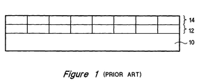
- Figure 1 shows a prior art array of active pixel sensors.
- An array of sensors 12 are formed over a substrate 10.
- An array of color filters 14 is formed over the array of sensors 12. Light passes through the color filters 14 and is received by the array of sensors 12.
- the sensors 12 typically conduct charge at a rate that is proportional to the intensity of the light received by the sensors 12.
- Circuitry located on the substrate 10 provides determination of the amount of charge conducted by the sensors 12. Therefore, the sensors 12 provide detection of the intensity of the received light.
- the array of color filters 14 includes filters which pass different wavelengths of light.
- the array of color filters 14 can include blue light, green light and red light filters.
- the blue light filters only passes blue light
- the green light filters only passes green light
- the red light filters only pass red light.
- each sensor of the array of sensors 12 corresponds with a single color filter of the array of color filters 14. Color detection can be obtained by knowing which sensor corresponds with which type of color filter.
- the active pixel sensor array of Figure 1 is inefficient because up to 70% of the photons within the received light are lost during the filtering process. That is, the color filters 14 attenuate the intensity of the light received by the array of sensors 12. Removing the color filters 14 increases the intensity of light received by the array of sensors 12. As a result, the color filters 14 reduce the signal to noise ratio of the electronic signals generated by the array of sensors 12.
- the active pixel sensor array of Figure 1 requires demosaicing. Each sensor of the array of sensors 12 detects the intensity of a particular color of light. Each sensor is physically displaced from all of the other sensors of the array of sensors 12. Therefore, special image processing (demosaicing) is required for determination of a representation of the color intensity received by the array of sensors 12 at each particular pixel location.
- an array of active pixel sensors which provide efficient absorption of photons within light received by the array of active pixel sensors, and be able to detect the color of received light. It is also desirable that the array of active pixel sensors be manufacturable without an array of color filters and not require demosaicing.
- the present invention is a color detection active pixel sensor which provides efficient absorption of photons of light received by the color active detection pixel sensor while providing detection of the color of the received light.
- the color detection is accomplished without color filters and does not require demosaicing.
- a first embodiment of the invention includes a multiple-photosensor structure.
- the multiple-photosensor structure includes a substrate.
- a first photosensor is formed adjacent to the substrate.
- a first pixel electrode of the first photosensor is electrically connected to the substrate.
- a first transparent conductive layer is formed adjacent to the first photosensor.
- the first transparent conductive layer electrically connects a first outer electrode of the first photosensor to the substrate.
- a second photosensor is adjacent to the first transparent conductive layer.
- a second pixel electrode of the second photosensor is electrically connected to the substrate through the first transparent conductive layer.
- a second transparent conductive layer is adjacent to the second photosensor.
- the second transparent conductive layer electrically connects a second outer electrode of the second photosensor to the substrate.
- a second embodiment of the invention is similar to the first embodiment.
- the second embodiment includes a third photosensor formed adjacent to the second transparent conductive layer.
- a third pixel electrode of the third photosensor is electrically connected to the substrate through the second transparent conductive layer.
- a third transparent conductive layer is formed adjacent to the third photosensor.
- the third transparent conductive layer electrically connects a third outer electrode of the third photosensor to the substrate.
- a third embodiment of the invention is similar to the first embodiment.
- the third embodiment includes the first photosensor detecting a first range of wavelengths of light.
- a fourth embodiment of the invention is similar to the first embodiment.
- the fourth embodiment includes the second photosensor detecting a second range of wavelengths of light.
- a fifth embodiment of the invention is similar to the second embodiment.
- the fifth embodiment includes the third photosensor detecting a third range of wavelengths of light.
- the invention is embodied in a color detection active pixel sensor which provides efficient absorption of photons of light received by the color active detection pixel sensor while providing detection of the color of the received light.
- the color detection is accomplished without color filters and does not require demosaicing.
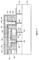
- Figure 2 shows an embodiment of the invention.
- the embodiment includes a substrate 200.
- An interconnection layer 210 is formed adjacent to the substrate 200.
- a first photosensor including a first pixel electrode 222, a first I-layer 224 and an outer layer 226 is formed adjacent to the interconnection layer 210.
- the interconnection layer 210 includes a first conductive interconnect 230 which electrically connects the first pixel electrode 222 of the first photosensor to the substrate 200.
- a first transparent conductor 240 electrically connects a first outer pixel electrode of the first photosensor to the substrate 200 through a second conductive interconnect 250.
- the first pixel electrode 222 typically includes an inner metal section 228.
- the embodiment further includes a second photosensor.
- the second photosensor includes a second pixel electrode 252, a second I-layer 254 and a second outer layer 256.
- the second photosensor is formed adjacent to the first transparent conductor 240.
- the first transparent conductor 240 electrically connects the second pixel electrode 252 of the second photosensor to the substrate 200.
- a second transparent conductor 258 electrically connects a second outer pixel electrode of the second photosensor to the substrate 200 through a third conductive interconnect 260.
- the embodiment can also include a third photosensor.
- the third photosensor includes a third pixel electrode 262, a third I-layer 264 and a third outer layer 266.
- the third photosensor is formed adjacent to the second transparent conductor 258.
- the second transparent conductor 258 electrically connects the third pixel electrode 262 of the third photosensor to the substrate 200.
- a third transparent conductor 268 electrically connects a third outer electrode of the third photosensor to the substrate 200 through a fourth conductive interconnect 270.
- Insulating regions 280 are generally included between each of the photosensors. The insulating regions provide isolation between the first photosensor, the second photosensor and the third photosensor.
- the photosensors conduct charge when the photosensors receive light.
- the substrate 200 generally includes sense circuitry and signal processing circuitry.
- the sense circuitry senses how much charge the image sensors have conducted.
- the amount of charge conducted represents the intensity of light received by the image sensors.
- the substrate 200 can be CMOS (complementary metal oxide silicon), BiCMOS or Bipolar.
- the substrate 200 can include various types of substrate technology including charged coupled devices.
- the interconnection layer 210 is a standard interconnection structure.
- the structure and methods of forming this interconnection layer 210 are well known in the field of electronic integrated circuit fabrication.
- the interconnection layer 210 can be a subtractive metal structure, or a single or dual damascene structure.
- the conductive interconnects 230, 240, 250 pass through the interconnection layer 210 and electrically connect the pixel electrodes 222, 252, 262 to the substrate 200.
- the fourth conductive interconnect 270 provides a reliable electrical connection between the third transparent conductor 268 and the substrate 200.
- the conductive interconnects 230, 240, 250, 270 are formed from tungsten. Tungsten is generally used during fabrication because tungsten can fill high aspect ratio holes. That is, tungsten can be used to form narrow and relatively long interconnections.
- the conductive interconnects 230, 240, 250, 270 are formed using a chemical vapor deposition (CVD) process. Other materials which can be used to form the conductive interconnects 230, 240, 250, 270 include copper, aluminum or any other electrically conductive material.
- the inner metal section 228 should include a thin conductive material.
- the inner metal section 228 may be formed, for example, from a degenerately doped semiconductor layer, aluminum, titanium, titanium nitride, copper or tungsten.
- the inner metal section 228 should be thin (approximately 500 Angstroms) and smooth.
- the inner metal section 228 should be smooth enough that any surface roughness is substantially less than the thickness of the first pixel electrode 222 formed over the inner metal section 228. To satisfy the smoothness requirement, polishing of the inner metal section 228 may be required.
- the inner metal section 228 can be optional. However, the inner metal section 228 has a lower resistance than the materials used to form the first pixel electrode 222. Therefore, the inner metal section 228 provides better current collection.
- the pixel electrodes 222, 252, 262 are generally formed from a doped semiconductor.
- the doped semiconductor can be an N-layer of amorphous silicon.
- the pixel electrodes 222, 252, 262 must be thick enough, and doped heavily enough that the pixel electrodes 222, 252, 262 do not fully deplete when biased during operation.
- the pixel electrodes 222, 252, 262 are typically doped with phosphorous.
- the pixel electrodes 222, 252, 262 are typically deposited using plasma etched chemical vapor deposition (PECVD).
- PECVD plasma etched chemical vapor deposition
- a silicon containing gas such as Si 2 H 6 or SiH 4
- Si 2 H 6 or SiH 4 is included when forming amorphous silicon pixel electrodes.
- the PECVD process is performed with a phosphorous containing gas (such as PH 3 ).
- the image photosensors can include an NIP sensor configuration.
- the pixel electrodes 222, 252, 262 are formed from a P-layer, and the outer layer sections 226,256, 266 of Figure 2 are replaced with N-layer sections.
- the first photosensor, the second photosensor and the third photosensor can each include different sensor configurations.
- the first photosensor could be a PIN image photosensor and the second photosensor could be an NIP photosensor.
- the I-layer sections 224, 254, 264 are generally formed from hydrogenated amorphous silicon.
- the I-layer sections 224, 254, 264 can be deposited using a PECVD process or a reactive sputtering process.
- the PECVD process must include a silicon containing gas.
- the deposition should be at a low enough temperature that hydrogen is retained within the film.
- the I-layer sections 224, 254, 264 typically on the order of one micron thick.
- the outer layer sections 226, 256, 266 are generally P-layers formed from amorphous silicon. Typically, the outer layer sections 226, 256, 266 are doped with Boron.
- the outer layer sections 226, 256, 266 can deposited using a PECVD process.
- the PECVD process is performed with a Boron containing gas.
- the Boron containing gas can be B 2 H 6 .
- a silicon containing gas is included when forming amorphous silicon P-layer outer layer sections 226, 256, 266.
- the thickness of the outer layer sections 226, 256, 266 must generally be controlled to ensure that the outer layer sections 226, 256, 266 do not absorb too much short wavelength (blue) light.
- the outer layer sections 226, 256, 266 can be made from microcrystalline silicon to provide the photosensors with better light collection.
- Another embodiment of the invention does not include outer layer sections 226, 256, 266.
- the outer layer sections 226, 256, 266 can be eliminated with proper selection of the composition of the material within the transparent conductors 240, 258, 268, and proper selection of the doping levels of the pixel electrodes 222, 252, 262.
- the transparent conductors 240, 258, 268 provide a conductive connection between a top surface of the I-layer sections 224, 254, 264 of the image sensors and the interconnection layer 210.
- Another embodiment of the invention does not include pixel electrodes 222, 252, 262.
- the pixel electrodes 222, 252, 262 can be eliminated with proper selection of the doping levels of the outer layer sections 226, 256, 266.
- the transparent conductors 240, 258, 268 provide a conductive connection between a top surface of the outer layer sections 226, 256, 266 of the image sensors and the interconnection layer 210.
- the insulating regions 280 provide isolation between the stacked image sensors formed by the pixel electrodes 222, 252, 262, the I-layer sections 224, 254, 264 and the outer layer sections 226, 256, 266. That is, the insulating regions 280 provide isolation between the stacked image sensors.
- the insulating regions 280 are typically formed from SiO 2 , Si 3 N 4 or a combination of SiO 2 and Si 3 N 4 .
- the pixel electrodes 222, 252, 262, the I-layer sections 224, 254, 264 and the outer layer sections 226, 256, 266 are generally formed from amorphous silicon.
- the pixel electrodes 222, 252, 262, the I-layer sections 224, 254, 264 and the outer layer sections 226, 256, 266 can also be formed from amorphous carbon, amorphous silicon carbide, amorphous germanium, or amorphous silicon-germanium. It should be understood that this list is not exhaustive.
- the transparent conductors 240, 258, 268 provide conductive connections between the outer layer sections 226, 256, 266 and the interconnection layer 210. Light must pass through the transparent conductors 240, 258, 268 which is received by the image sensors.
- the transparent conductors 240, 258, 268 are formed from an indium tin oxide.
- the transparent conductors 240, 258, 268 can also be formed from titanium nitride, thin silicide, or certain types of transition metal nitrides or oxides.
- Both the selection of the type of material to be used within the transparent conductors 240, 258, 268, and the determination of the desired thickness of the transparent conductors 240, 258, 268, are based upon minimizing the optical reflection of light received by the image sensor. Minimization of the reflection of light received by the image sensor helps to optimize the amount of light detected by the image sensor.
- the transparent conductors 240, 258, 268 can be deposited by a sputtering process. Deposition through sputtering is well known in the art of integrated circuit fabrication.
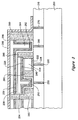
- Figure 3 shows another embodiment of the invention. This embodiment is similar to the embodiment of Figure 2, but includes structural differences due to differences in the processes used to form the embodiments.
- the outer layer 226 extends underneath the first transparent conductor 240
- the second outer layer 256 extends underneath the second transparent conductor 258
- the third outer layer 266 extends underneath the third transparent conductor 268.
- the embodiment of Figure 3 includes the edges of the first outer electrode aligning with edges of the first transparent conductive layer. It is not required that each of the photosensor include this structure.
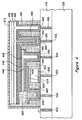
- Figure 4 shows another embodiment of the invention. This embodiment is similar to the embodiments of Figure 2 and Figure 3.
- This embodiment includes the first transparent conductive layer being divided into a inner first transparent conductive layer 430 and an outer first transparent conductive layer 442.
- the second transparent conductive layer is divided into an inner second transparent conductive layer 450 and an outer second transparent conductive layer 462.
- a first insulating layer 434 is located between the inner first transparent conductive layer 430 and the outer first transparent conductive layer 442.
- a second insulating layer 454 is located between the inner second transparent conductive layer 450 and the outer second transparent conductive layer 462. Either the first insulating layer 434 or the second insulating layer 454 can be eliminated.
- a first photosensor including a first pixel electrode 422, a first I-layer 424 and an outer layer 426 is formed adjacent to the interconnection layer 210.
- the interconnection layer 210 includes a first conductive interconnect 420 which electrically connects the first pixel electrode 422 of the first photosensor to the substrate 200.
- the inner first transparent conductive layer 430 electrically connects a first outer pixel electrode of the first photosensor to the substrate 200 through a second conductive interconnect 432.
- the first pixel electrode 422 typically includes an inner metal section 428.
- This embodiment also includes a second photosensor.
- the second photosensor includes a second pixel electrode 444, a second I-layer 446 and a second outer layer 448.
- the second photosensor is formed adjacent to the outer first transparent conductive layer 442.
- the outer first transparent conductive layer 442 electrically connects the second pixel electrode 444 of the second photosensor to the substrate 200 through a third conductive interconnect 440.
- the inner second transparent conductive layer 450 electrically connects a second outer pixel electrode of the second photosensor to the substrate 200 through a fourth conductive interconnect 452.
- the embodiment can also include a third photosensor.
- the third photosensor includes a third pixel electrode 464, a third I-layer 466 and a third outer layer 468.
- the third photosensor is formed adjacent to the outer second transparent conductive layer 462.
- the outer second transparent conductive layer 462 electrically connects the third pixel electrode 464 of the third photosensor to the substrate 200 through a fifth conductive interconnect 460.
- a third transparent conductor 470 electrically connects a third outer electrode of the third photosensor to the substrate 200 through a sixth conductive interconnect 472.
- Insulating regions 480 are generally included between each of the photosensors.
- the insulating regions provide isolation between the first photosensor, the second photosensor and the third photosensor.
- the insulating regions 480, the first insulating layer 434 and the second insulating layer 454, can each be formed from the same or different types of dielectrics.
- the first insulating layer 434 provides insulation between the inner first transparent conductive layer 430 and the outer first transparent conductive layer 442.
- the second insulating layer 454 provides insulation between the inner second transparent conductive layer 450 and the outer second transparent conductive layer 462.
- each photosensor of the embodiments described in Figure 2, Figure 3 and Figure 4 conducts charge when the photosensor receives light.
- Each photosensor can be formed to detect varying wavelengths of light depending upon the structure of the photosensor. In particular, the thickness of the I-layer of each photosensor can be adjusted to vary the wavelengths of light detectable by the photosensor.
- a charge sensor can be connected to the outer electrode of each of the photosensors of the invention to measure the charge conducted by each photosensor, and therefore, determine the intensity of light received by each photosensor.
- the circuitry required to detect the charge conducted by a photosensor is well known in the art of electronics.
- the circuitry required to detect the charge conducted by each photosensor can be located on the substrate 200.
- the light absorption characteristics of a particular photosensor is dependent upon an absorption length L0 associated with the photosensor.
- the absorption length L0 is a constant which is generally unique for a particular material.
- the absorption length L0 of a given material will typically vary depending upon the wavelength of the light being receive by the photosensor.
- Figure 5 is a plot which depicts the absorption length L0 of amorphous silicon for wavelengths of light varying from 4000 Angstroms to about 7000 Angstroms.
- Material other than amorphous silicon can be used to form the photosensors of the invention.
- the absorption length of alternate materials will vary depending upon the characteristics of the materials.
- the absorption length L0 varies from about 200 Angstroms to about 6000 Angstroms for wavelengths between 4000 Angstroms and 7000 Angstroms.
- the amount of light absorbed by the photosensor can be determined by the following relationship:
- the plot of Figure 5 shows that the absorption length L0 for amorphous silicon is about 600 Angstroms for blue light having a wavelength of about 4500 Angstroms.
- the amount of blue light absorbed by a photosensor having an I-layer width of 600 Angstroms is about I 0 (1- e- (1) ) or about 63% of the blue light received by the photosensor.
- the amount of red light having a wavelength of about 6500 Angstroms which is absorbed by the photosensor having an I-layer thickness of 600 Angstroms is about I 0 (1-e- (600/4000) ) , which is a substantially smaller than the amount of blue light absorbed.
- An embodiment of the invention includes the thickness of the third I-layer of the third photosensor being between approximately 500 and 800 Angstroms.
- This embodiment includes the third photosensor detecting blue light having a wavelength of about 4500 Angstroms. The light having wavelengths greater than that of blue light pass through the third photosensor substantially undetected or absorbed.
- Another embodiment of the invention includes the thickness of the second I-layer of the second photosensor being between approximately 1200 and 1800 Angstroms.
- This embodiment includes the second photosensor detecting green light having a wavelength of about 5500 Angstroms. The light having wavelengths greater than that of green light pass through the second photosensor substantially undetected or absorbed.
- Another embodiment of the invention includes the thickness of the first I-layer of the first photosensor being between approximately 2500 and 3500 Angstroms.
- This embodiment includes the second photosensor detecting red light having a wavelength of about 6500 Angstroms.
- the thickness of the I-layer can be controlled by controlling the amount of I-layer material deposited during the formation of the photosensor.
- the light detected by the photosensor does not have to be visible light.
- any or all of the sensors can be configured to detect near infrared (IR) or ultraviolet (UV) light.
- FIGS 6-8 are flow charts showing processing steps which can be used to fabricate the embodiments shown in Figure 2 and Figure 3.
- Figure 6 is a flow chart which shows processing steps which can be used to form the embodiment of the invention shown in Figure 2.
- a first step 605 includes depositing a metal layer, a first electrode layer, a first I-layer and a first outer layer over an interconnection layer 210 which is formed over a substrate 200.
- the structure and methods of forming the substrate 200 and the interconnection layer 210 are well known in the field of electronic integrated circuit fabrication.
- the interconnection layer 210 is typically formed from a silicon oxide or a silicon nitride.
- the interconnection layer 210 includes conductive interconnects 230, 250, 260, 270 which are formed using a chemical vapor deposition (CVD) process.
- CVD chemical vapor deposition
- the conductive interconnects 230, 250, 260, 270 are formed from tungsten because tungsten can fill high aspect ratio holes.
- the electrode layer can be implemented with an N-layer or a P-layer.
- the electrode layer can be titanium nitride, tungsten, titanium or other thin film conductors.
- the electrode layer is typically deposited using PECVD.
- the PECVD is performed with a phosphorous containing gas.
- the phosphorous containing gas can be PH 3 .
- the phosphorous containing gas can be PH 3 .
- a silicon containing gas, such as Si 2 H 6 or SiH 4 is included when forming amorphous silicon electrode layer.
- the I-layer is generally deposited using a PECVD or reactive sputtering process.
- the PECVD must include a silicon containing gas.
- the deposition should be at a low enough temperature that hydrogen is retained within the film.
- the outer layer can also be deposited using PECVD.
- the PECVD is performed with a boron containing gas.
- the boron containing gas can be B 2 H 6 .
- a silicon containing gas is included when forming an amorphous silicon outer layer.
- a second step 610 includes etching the deposited metal layer, the first electrode layer, the first I-layer and the first outer layer to form the first photosensor according to predetermined pattern.
- an array of active pixel sensors includes an array of first photosensors. Etching the layers forms the first pixel electrode 222, the first I-layer 224 and the outer layer 226 of the first photosensor.
- a third step 615 includes depositing a dielectric such as an oxide, planarizing the oxide and etching a via in the oxide to allow biasing of the first photosensor.
- the oxide is typically deposited through a PECVD process.
- the oxide is typically formed from SiO 2 .
- the oxide forms the insulating regions 280 between the first photosensor, the second photosensor and the third photosensor.
- the via is etched where the first transparent conductor 240 electrically connects the first pixel electrode of the first photosensor to the substrate 200.
- a fourth step 620 includes depositing the first transparent conductor layer 240.
- the first transparent conductor 240 is formed from an indium tin oxide.
- the first transparent conductor 240 can also be formed from titanium nitride, thin silicide, or certain types of conductive transition metal nitrides or oxides.
- the first transparent conductor layer 240 is generally deposited through reactive sputtering. However, the first transparent conductor layer 240 can also be grown by evaporation. If the first transparent conductor layer 240 is formed from titanium nitride, then typically a CVD process or a sputtering process must be used to deposit the first transparent conductor layer 240.
- a fifth step 625 includes depositing a second electrode layer, a second I-layer and a second outer layer over the first transparent conductor layer 240.
- the second electrode layer can be implemented with an N-layer or a P-layer.
- the second electrode layer can be a conductive nitride, like, titanium nitride.
- the second electrode layer is typically deposited using PECVD.
- the PECVD is performed with a phosphorous containing gas.
- the phosphorous containing gas can be PH 3 .
- the phosphorous containing gas can be PH 3 .
- a silicon containing gas, such as Si 2 H 6 or SiH 4 is included when forming an amorphous silicon electrodes layer.
- the second I-layer is generally deposited using a PECVD or reactive sputtering process.
- the PECVD must include a silicon containing gas.
- the deposition should be at a low enough temperature that hydrogen is retained within the film.
- the second outer layer can also be deposited using PECVD.
- the PECVD is performed with a boron containing gas.
- the boron containing gas can be B 2 H 6 .
- a silicon containing gas is included when forming an amorphous silicon outer layer.
- a sixth step 630 includes etching the deposited second electrode layer, the second I-layer and the second outer layer to form the second photosensor according to predetermined pattern.
- an array of active pixel sensors includes an array of second photosensors. Etching the layers forms the second pixel electrode 252, the second I-layer 254 and the second outer layer 256 of the second photosensor.
- a seventh step 635 includes depositing a dielectric such as an oxide, planarizing the oxide and etching a via in the oxide to allow biasing of the second photosensor.
- the oxide is typically deposited through a PECVD process.
- the oxide is typically formed from SiO 2 .
- the oxide forms the insulating regions 280 between the first photosensor, the second photosensor and the third photosensor.
- the via is etched where the second transparent conductor 258 electrically connects the second pixel electrode 252 of the second photosensor to the substrate 200.
- An eighth step 640 includes depositing the second transparent conductor layer 258.
- the second transparent conductor layer 258 is formed from an indium tin oxide.
- the second transparent conductor layer 258 can also be formed from titanium nitride, thin silicide, or certain types of transition metal nitrides or oxides.
- the second transparent conductor layer 258 is generally deposited through reactive sputtering. However, the second transparent conductor layer 258 can also be grown by evaporation. If the second transparent conductor layer 258 is formed from titanium nitride, then typically a CVD process or a sputtering process must be used to deposit the second transparent conductor layer 258.
- a ninth step 645 includes depositing a third electrode layer, a third I-layer and a third outer layer over the second transparent conductor layer 258.
- the third electrode layer can be implemented with an N-layer or a P-layer.
- the third electrode layer can be a conductive nitride, like, titanium nitride.
- the third electrode layer is typically deposited using PECVD.
- the PECVD is performed with a phosphorous containing gas.
- the phosphorous containing gas can be PH 3 .
- the phosphorous containing gas can be PH 3 .
- a silicon containing gas, such as Si 2 H 6 or SiH 4 is included when forming an amorphous silicon electrode layer.
- the third I-layer is generally deposited using a PECVD or reactive sputtering process.
- the PECVD must include a silicon containing gas.
- the deposition should be at a low enough temperature that hydrogen is retained within the film.
- the third outer layer can also be deposited using PECVD.
- the PECVD is performed with a boron containing gas.
- the boron containing gas can be B 2 H 6 .
- a silicon containing gas is included when forming an amorphous silicon outer layer.
- a tenth step 650 includes etching the deposited third electrode layer, the third I-layer and the third outer layer to form the third photosensor according to predetermined pattern.
- an array of active pixel sensors includes an array of third photosensors. Etching the layers forms the third pixel electrode 262, the third I-layer 264 and the third outer layer 266 of the third photosensor.
- An eleventh step 655 includes depositing an oxide, planarizing the oxide and etching a via in the oxide to allow biasing of the third photosensor.
- the oxide is typically deposited through a PECVD process.
- the oxide is typically formed from SiO 2 .
- the oxide forms the insulating regions 280 between the first photosensor, the third photosensor and the third photosensor.
- the via is etched where the third transparent conductor 268 electrically connects the third pixel electrode 262 of the third photosensor to the substrate 200.
- a twelfth step 660 includes depositing the third transparent conductor layer 268.
- the third transparent conductor layer 268 is formed from an indium tin oxide.
- the third transparent conductor layer 268 can also be formed from titanium nitride, thin silicide, or certain types of transition metal nitrides or oxides.
- the third transparent conductor layer 268 is generally deposited through reactive sputtering. However, the third transparent conductor layer 268 can also be grown by evaporation. If the third transparent conductor layer 268 is formed from titanium nitride, then typically a CVD process or a sputtering process must be used to deposit the third transparent conductor layer 268.
- Figure 7 is a flow chart which shows another set of processing steps which can be used to form the embodiment of the invention shown in Figure 2. This method allows for planarization of the insulating oxide regions.
- a first step 705 includes depositing a metal layer, a first electrode layer, a first I-layer and a first outer layer over an interconnection layer 210 which is formed over a substrate 200.
- the structure and methods of forming the substrate 200 and the interconnection layer 210 are well known in the field of electronic integrated circuit fabrication.
- the interconnection layer 210 is typically formed from a silicon oxide or a silicon nitride.
- the interconnection layer 210 includes conductive interconnects 230, 250, 260, 270 which are formed using a chemical vapor deposition (CVD) process.
- CVD chemical vapor deposition
- the conductive interconnects 230, 250, 260, 270 are formed from tungsten because tungsten can fill high aspect ratio holes.
- the electrode layer can be implemented with an N-layer or a P-layer.
- the electrode layer can be a conductive nitride, like, titanium nitride.
- the electrode layer is typically deposited using PECVD.
- the PECVD is performed with a phosphorous containing gas.
- the phosphorous containing gas can be PH 3 .
- the phosphorous containing gas can be PH 3 .
- a silicon containing gas, such as Si 2 H 6 or SiH 4 is included when forming amorphous silicon electrode layer.
- the I-layer is generally deposited using a PECVD or reactive sputtering process.
- the PECVD must include a silicon containing gas.
- the deposition should be at a low enough temperature that hydrogen is retained within the film.
- the outer layer can also be deposited using PECVD.
- the PECVD is performed with a boron containing gas.
- the boron containing gas can be B 2 H 6 .
- a silicon containing gas is included when forming an amorphous silicon outer layer.
- a second step 710 includes depositing a silicon nitride stop layer and etching the deposited metal layer, the first electrode layer, the first I-layer and the first outer layer to form the first photosensor according to a predetermined pattern.
- the silicon nitride stop layer is deposited because the silicon nitride stop layer provides for better control of planarization, and protects electrically active layer underneath the silicon nitride stop layer.
- an array of active pixel sensors includes an array of first photosensors. Etching the layers forms the first pixel electrode 222, the first I-layer 224 and the outer layer 226 of the first photosensor.
- a third step 715 includes depositing on oxide, planarizing the oxide and stripping any residual silicon nitride stop layer.
- the oxide is typically deposited through a PECVD process.
- the oxide is typically formed from SiO 2 .
- the oxide forms the insulating regions 280 between the first photosensor, the second photosensor and the third photosensor.
- residual silicon nitride stop layer may still reside over the formed pixels.
- the residual silicon nitride stop layer is typically stripped by an H 3 PO 4 wet solution.
- a fourth step 720 includes etching a via in the oxide to allow biasing of the first photosensor, and depositing the first transparent conductor layer 240.
- the via is etched where the first transparent conductor 240 electrically connects the first pixel electrode 222 of the first photosensor to the substrate 200.
- the first transparent conductor 240 is formed from an indium tin oxide.
- the first transparent conductor 240 can also be formed from titanium nitride, thin silicide, or certain types of transition metal nitrides or oxides.
- the first transparent conductor layer 240 is generally deposited through reactive sputtering. However, the first transparent conductor layer 240 can also be grown by evaporation. If the first transparent conductor layer 240 is formed from titanium nitride, then typically a CVD process or a sputtering process must be used to deposit the first transparent conductor layer 240.
- a fifth step 725 includes depositing a second electrode layer, a second I-layer and a second outer layer over the first transparent conductor layer 240.
- the second electrode layer can be implemented with an N-layer or a P-layer.
- the second electrode layer can be a conductive nitride, like, titanium nitride.
- the second electrode layer is typically deposited using PECVD.
- the PECVD is performed with a phosphorous containing gas.
- the phosphorous containing gas can be PH 3 .
- the phosphorous containing gas can be PH 3 .
- a silicon containing gas, such as Si 2 H 6 or SiH 4 is included when forming an amorphous silicon electrodes layer.
- the second I-layer is generally deposited using a PECVD or reactive sputtering process.
- the PECVD must include a silicon containing gas.
- the deposition should be at a low enough temperature that hydrogen is retained within the film.
- the second outer layer can also be deposited using PECVD.
- the PECVD is performed with a boron containing gas.
- the boron containing gas can be B 2 H 6 .
- a silicon containing gas is included when forming an amorphous silicon outer layer.
- a sixth step 730 includes depositing an silicon nitride stop layer and etching the deposited second electrode layer, the second I-layer and the second outer layer to form the second photosensor according to predetermined pattern.
- the silicon nitride stop layer is deposited because the silicon nitride stop layer provides for better control of planarization, and protects electrically active layers beneath the silicon nitride stop layer.
- an array of active pixel sensors includes an array of second photosensors. Etching the layers forms the second pixel electrode 252, the second I-layer 254 and the second outer layer 256 of the second photosensor.
- a seventh step 735 includes depositing a dielectric such as an oxide, planarizing the oxide and stripping any residual silicon nitride stop layer.
- the oxide is typically deposited through a PECVD process.
- the oxide is typically formed from SiO 2 .
- the oxide forms the insulating regions 280 between the first photosensor, the second photosensor and the third photosensor.
- residual silicon nitride stop layer may still reside over the formed pixels.
- the residual silicon nitride stop layer is typically stripped by an H 3 PO 4 wet solution.
- An eighth step 740 includes etching a via in the oxide to allow biasing of the second photosensor, and depositing the second transparent conductor layer 258.
- the via is etched where the second transparent conductor 258 electrically connects the second pixel electrode 252 of the second photosensor to the substrate 200.
- the second transparent conductor layer 258 is formed from an indium tin oxide.
- the second transparent conductor layer 258 can also be formed from titanium nitride, thin silicide, or certain types of transition metal nitrides or oxides.
- the second transparent conductor layer 258 is generally deposited through reactive sputtering. However, the second transparent conductor layer 258 can also be grown by evaporation. If the second transparent conductor layer 258 is formed from titanium nitride, then typically a CVD process or a sputtering process must be used to deposit the second transparent conductor layer 258.
- a ninth step 745 includes depositing a third electrode layer, a third I-layer and a third outer layer over the second transparent conductor layer 258.
- the third electrode layer can be implemented with an N-layer or a P-layer.
- the third electrode layer can be a conductive nitride, like, titanium nitride.
- the third electrode layer is typically deposited using PECVD.
- the PECVD is performed with a phosphorous containing gas.
- the phosphorous containing gas can be PH 3 .
- the phosphorous containing gas can be PH 3 .
- a silicon containing gas, such as Si 2 H 6 or SiH 4 is included when forming an amorphous silicon electrode layer.
- the third I-layer is generally deposited using a PECVD or reactive sputtering process.
- the PECVD must include a silicon containing gas.
- the deposition should be at a low enough temperature that hydrogen is retained within the film.
- the third outer layer can also be deposited using PECVD.
- the PECVD is performed with a boron containing gas.
- the boron containing gas can be B 2 H 6 .
- a silicon containing gas is included when forming an amorphous silicon outer layer.
- a tenth step 750 includes depositing an silicon nitride stop layer and etching the deposited third electrode layer, the third I-layer and the third outer layer to form the third photosensor according to predetermined pattern.
- the silicon nitride stop layer is deposited because the silicon nitride stop layer provides for better control of planarization, and protects electrically active layers beneath the silicon nitride stop layer.
- an array of active pixel sensors includes an array of third photosensors. Etching the layers forms the third pixel electrode 262, the third I-layer 264 and the third outer layer 266 of the third photosensor.
- An eleventh step 755 includes depositing a dielectric such as an oxide, planarizing the oxide and stripping any residual silicon nitride stop layer.
- the oxide is typically deposited through a PECVD process.
- the oxide is typically formed from SiO 2 .
- the oxide forms the insulating regions 280 between the first photosensor, the third photosensor and the third photosensor.
- residual silicon nitride stop layer may still reside over the formed pixels.
- the residual silicon nitride stop layer is typically stripped by an H 3 PO 4 wet solution.
- a twelfth step 760 includes etching a via in the oxide to allow biasing of the third photosensor, and depositing the third transparent conductor layer 268.
- the via is etched where the third transparent conductor 268 electrically connects the third pixel electrode 262 of the third photosensor to the substrate 200.
- the third transparent conductor layer 268 is formed from an indium tin oxide.
- the third transparent conductor layer 268 can also be formed from titanium nitride, thin silicide, or certain types of transition metal nitrides or oxides.
- the third transparent conductor layer 268 is generally deposited through reactive sputtering. However, the third transparent conductor layer 268 can also be grown by evaporation. If the third transparent conductor layer 268 is formed from titanium nitride, then typically a CVD process or a sputtering process must be used to deposit the third transparent conductor layer 268.
- the silicon nitride stop layer of the third step 715, the sixth step 730, and the tenth step 750 can be replaced by any material which provides the required etching selectivity of the isolation dielectric, and can be stripped by a method that is selective relative to the dielectric and the photosensor films.
- FIG 8 is a flow chart which shows processing steps which can be used to form the embodiment of the invention shown in Figure 3.
- a first step 805 includes depositing a metal layer, a first electrode layer and a first I-layer over an interconnection layer 210 which is formed over a substrate 200.
- the structure and methods of forming the substrate 200 and the interconnection layer 210 are well known in the field of electronic integrated circuit fabrication.
- the interconnection layer 210 is typically formed from a silicon oxide or a silicon nitride.
- the interconnection layer 210 includes conductive interconnects 230, 250, 260, 270 which are formed using a chemical vapor deposition (CVD) process.
- CVD chemical vapor deposition
- the conductive interconnects 230, 250, 260, 270 are formed from tungsten because tungsten can fill high aspect ratio holes.
- the electrode layer can be implemented with an N-layer or a P-layer.
- the electrode layer can be titanium nitride, tungsten, titanium or other thin film conductors.
- the electrode layer is typically deposited using PECVD.
- the PECVD is performed with a phosphorous containing gas.
- the phosphorous containing gas can be PH 3 .
- the phosphorous containing gas can be PH 3 .
- a silicon containing gas, such as Si 2 H 6 or SiH 4 is included when forming amorphous silicon electrode layer.
- the I-layer is generally deposited using a PECVD or reactive sputtering process.
- the PECVD must include a silicon containing gas.
- the deposition should be at a low enough temperature that hydrogen is retained within the film.
- a second step 810 includes etching the deposited metal layer, the first electrode layer and the first I-layer to form the first photosensor according to predetermined pattern.
- an array of active pixel sensors includes an array of first photosensors. Etching the layers forms the first pixel electrode 222 and the first I-layer 224 of the first photosensor.
- a third step 815 includes depositing on oxide, planarizing the oxide and etching a via in the oxide to allow biasing of the first photosensor.
- the oxide is typically deposited through a PECVD process.
- the oxide is typically formed from SiO 2 .
- the oxide forms the insulating regions 280 between the first photosensor, the second photosensor and the third photosensor.
- the via is etched where the first transparent conductor 240 electrically connects the first pixel electrode 222 of the first photosensor to the substrate 200.
- a fourth step 820 includes depositing a first outer layer and the first transparent conductor layer 240.
- the outer layer can be deposited using PECVD.
- the PECVD is performed with a boron containing gas.
- the boron containing gas can be B 2 H 6 .
- a silicon containing gas is included when forming an amorphous silicon outer layer.
- the first transparent conductor 240 is formed from an indium tin oxide.
- the first transparent conductor 240 can also be formed from titanium nitride, thin silicide, or certain types of transition metal nitrides or oxides.
- the first transparent conductor layer 240 is generally deposited through reactive sputtering. However, the first transparent conductor layer 240 can also be grown by evaporation. If the first transparent conductor layer 240 is formed from titanium nitride, then typically a CVD process or a sputtering process must be used to deposit the first transparent conductor layer 240.
- a fifth step 825 includes depositing a second electrode layer and a second I-layer over the first transparent conductor layer 240.
- the second electrode layer can be implemented with an N-layer or a P-layer.
- the second electrode layer can be a conductive nitride, like, titanium nitride.
- the second electrode layer is typically deposited using PECVD.
- the PECVD is performed with a phosphorous containing gas.
- the phosphorous containing gas can be PH 3 .
- the phosphorous containing gas can be PH 3 .
- a silicon containing gas, such as Si 2 H 6 or SiH 4 is included when forming an amorphous silicon electrodes layer.
- the second I-layer is generally deposited using a PECVD or reactive sputtering process.
- the PECVD must include a silicon containing gas.
- the deposition should be at a low enough temperature that hydrogen is retained within the film.
- a sixth step 830 includes etching the deposited second electrode layer and the second I-layer to form the second photosensor according to predetermined pattern.
- an array of active pixel sensors includes an array of second photosensors. Etching the layers forms the second pixel electrode 252, the second I-layer 254 and the second outer layer 256 of the second photosensor.
- a seventh step 835 includes depositing on oxide, planarizing the oxide and etching a via in the oxide to allow biasing of the second photosensor.
- the oxide is typically deposited through a PECVD process.
- the oxide is typically formed from SiO 2 .
- the oxide forms the insulating regions 280 between the first photosensor, the second photosensor and the third photosensor.
- the via is etched where the second transparent conductor 258 electrically connects the second pixel electrode 252 of the second photosensor to the substrate 200.
- An eighth step 840 includes depositing a second outer layer and the second transparent conductor layer 258.
- the second outer layer can be deposited using PECVD.
- the PECVD is performed with a boron containing gas.
- the boron containing gas can be B 2 H 6 .
- a silicon containing gas is included when forming an amorphous silicon outer layer.
- the second transparent conductor layer 258 is formed from an indium tin oxide.
- the second transparent conductor layer 258 can also be formed from titanium nitride, thin silicide, or certain types of transition metal nitrides or oxides.
- the second transparent conductor layer 258 is generally deposited through reactive sputtering. However, the second transparent conductor layer 258 can also be grown by evaporation. If the second transparent conductor layer 258 is formed from titanium nitride, then typically a CVD process or a sputtering process must be used to deposit the second transparent conductor layer 258.
- a ninth step 845 includes depositing a third electrode layer and a third I-layer over the second transparent conductor layer 258.
- the third electrode layer can be implemented with an N-layer or a P-layer.
- the third electrode layer can be a conductive nitride, like, titanium nitride.
- the third electrode layer is typically deposited using PECVD.
- the PECVD is performed with a phosphorous containing gas.
- the phosphorous containing gas can be PH 3 .
- the phosphorous containing gas can be PH 3 .
- a silicon containing gas, such as Si 2 H 6 or SiH 4 is included when forming an amorphous silicon electrode layer.
- the third I-layer is generally deposited using a PECVD or reactive sputtering process.
- the PECVD must include a silicon containing gas.
- the deposition should be at a low enough temperature that hydrogen is retained within the film.
- the third outer layer can also be deposited using PECVD.
- the PECVD is performed with a boron containing gas.
- the boron containing gas can be B 2 H 6 .
- a silicon containing gas is included when forming an amorphous silicon outer layer.
- a tenth step 850 includes etching the deposited third electrode layer and the third I-layer to form the third photosensor according to predetermined pattern.
- an array of active pixel sensors includes an array of third photosensors. Etching the layers forms the third pixel electrode 262 and the third I-layer 264 of the third photosensor.
- An eleventh step 855 includes depositing an oxide, planarizing the oxide and etching a via in the oxide to allow biasing of the third photosensor.
- the oxide is typically deposited through a PECVD process.
- the oxide is typically formed from SiO 2 .
- the oxide forms the insulating regions 280 between the first photosensor, the third photosensor and the third photosensor.
- the via is etched where the third transparent conductor 268 electrically connects the third pixel electrode 262 of the third photosensor to the substrate 200.
- a twelfth step 860 includes depositing a third outer layer and the third transparent conductor layer 268.
- the third outer layer can be deposited using PECVD.
- the PECVD is performed with a boron containing gas.
- the boron containing gas can be B 2 H 6 .
- a silicon containing gas is included when forming an amorphous silicon outer layer.
- the third transparent conductor layer 268 is formed from an indium tin oxide.
- the third transparent conductor layer 268 can also be formed from titanium nitride, thin silicide, or certain types of transition metal nitrides or oxides.
- the third transparent conductor layer 268 is generally deposited through reactive sputtering. However, the third transparent conductor layer 268 can also be grown by evaporation. If the third transparent conductor layer 268 is formed from titanium nitride, then typically a CVD process or a sputtering process must be used to deposit the third transparent conductor layer 268.
- each conductive layer includes the deposition of a conductive layer, an insulating layer and another conductive layer.
Landscapes
- Solid State Image Pick-Up Elements (AREA)
- Light Receiving Elements (AREA)
Abstract
Description
- The present invention relates to a multiple-photosensor structure. In particular, it relates to a stacked multiple active pixel photo sensor that includes independent electrical connections to each photosensor, allowing multiple color detection.
- An array of photo pixel sensors detect the intensity of light received by the photo pixel sensors. The photo pixel sensors typically generate electronic signals that have amplitudes that are proportionate to the intensity of the light received by the photo pixel sensors. The photo pixel sensors can convert an optical image into a set of electronic signals. The electronic signals may represent intensities of colors of light received by the photo pixel sensors. The electronic signals can be conditioned and sampled to allow image processing.
- Integration of the photo pixel sensors with signal processing circuitry is becoming more important because integration enables miniaturization and simplification of imaging systems. Integration of photo pixel sensors along with analog and digital signal processing circuitry allows electronic imaging systems to be low cost, compact and require low power.
- Historically, photo pixel sensors have predominantly been charged coupled devices (CCDs). CCDs are relatively small and can provide a high-fill factor. However, CCDs are very difficult to integrate with digital and analog circuitry. Further, CCDs dissipate large amounts of power and suffer from image smearing problems.
- An alternative to CCD sensors are active pixel sensors. Active pixel sensors can be fabricated using standard CMOS processes. Therefore, active pixel sensors can easily be integrated with digital and analog signal processing circuitry. Further, CMOS circuits dissipate small amounts of power.
- Figure 1 shows a prior art array of active pixel sensors. An array of
sensors 12 are formed over asubstrate 10. An array ofcolor filters 14 is formed over the array ofsensors 12. Light passes through thecolor filters 14 and is received by the array ofsensors 12. Thesensors 12 typically conduct charge at a rate that is proportional to the intensity of the light received by thesensors 12. Circuitry located on thesubstrate 10 provides determination of the amount of charge conducted by thesensors 12. Therefore, thesensors 12 provide detection of the intensity of the received light. - The array of
color filters 14 includes filters which pass different wavelengths of light. For example, the array ofcolor filters 14 can include blue light, green light and red light filters. The blue light filters only passes blue light, the green light filters only passes green light and the red light filters only pass red light. Generally, each sensor of the array ofsensors 12 corresponds with a single color filter of the array ofcolor filters 14. Color detection can be obtained by knowing which sensor corresponds with which type of color filter. - The active pixel sensor array of Figure 1 is inefficient because up to 70% of the photons within the received light are lost during the filtering process. That is, the
color filters 14 attenuate the intensity of the light received by the array ofsensors 12. Removing thecolor filters 14 increases the intensity of light received by the array ofsensors 12. As a result, thecolor filters 14 reduce the signal to noise ratio of the electronic signals generated by the array ofsensors 12. - The active pixel sensor array of Figure 1 requires demosaicing. Each sensor of the array of
sensors 12 detects the intensity of a particular color of light. Each sensor is physically displaced from all of the other sensors of the array ofsensors 12. Therefore, special image processing (demosaicing) is required for determination of a representation of the color intensity received by the array ofsensors 12 at each particular pixel location. - It is desirable to have an array of active pixel sensors which provide efficient absorption of photons within light received by the array of active pixel sensors, and be able to detect the color of received light. It is also desirable that the array of active pixel sensors be manufacturable without an array of color filters and not require demosaicing.
- The present invention is a color detection active pixel sensor which provides efficient absorption of photons of light received by the color active detection pixel sensor while providing detection of the color of the received light. The color detection is accomplished without color filters and does not require demosaicing.
- A first embodiment of the invention includes a multiple-photosensor structure. The multiple-photosensor structure includes a substrate. A first photosensor is formed adjacent to the substrate. A first pixel electrode of the first photosensor is electrically connected to the substrate. A first transparent conductive layer is formed adjacent to the first photosensor. The first transparent conductive layer electrically connects a first outer electrode of the first photosensor to the substrate. A second photosensor is adjacent to the first transparent conductive layer. A second pixel electrode of the second photosensor is electrically connected to the substrate through the first transparent conductive layer. A second transparent conductive layer is adjacent to the second photosensor. The second transparent conductive layer electrically connects a second outer electrode of the second photosensor to the substrate.
- A second embodiment of the invention is similar to the first embodiment. The second embodiment includes a third photosensor formed adjacent to the second transparent conductive layer. A third pixel electrode of the third photosensor is electrically connected to the substrate through the second transparent conductive layer. A third transparent conductive layer is formed adjacent to the third photosensor. The third transparent conductive layer electrically connects a third outer electrode of the third photosensor to the substrate.
- A third embodiment of the invention is similar to the first embodiment. The third embodiment includes the first photosensor detecting a first range of wavelengths of light.
- A fourth embodiment of the invention is similar to the first embodiment. The fourth embodiment includes the second photosensor detecting a second range of wavelengths of light.
- A fifth embodiment of the invention is similar to the second embodiment. The fifth embodiment includes the third photosensor detecting a third range of wavelengths of light.
- Other aspects and advantages of the present invention will become apparent from the following detailed description, taken in conjunction with the accompanying drawings, illustrating preferred embodiments of the invention.
- Figure 1 shows a cross-section of a prior art array of photosensors.
- Figure 2 shows an embodiment of the invention.
- Figure 3 shows another embodiment of the invention.
- Figure 4 shows another embodiment of the invention.
- Figure 5 is a curve which depicts the relationship between the thickness of an I-layer of a PIN photosensor and the wavelength of light absorbed by the I-layer.
- Figure 6 is a flow chart which shows processing steps which can be used to form the embodiment of the invention shown in Figure 2.
- Figure 7 is a flow chart which shows another set of processing steps which can be used to form the embodiment of the invention shown in Figure 2.
- Figure 8 is a flow chart which shows processing steps which can be used to form the embodiment of the invention shown in Figure 3.
-
- As shown in the drawings for purposes of illustration, the invention is embodied in a color detection active pixel sensor which provides efficient absorption of photons of light received by the color active detection pixel sensor while providing detection of the color of the received light. The color detection is accomplished without color filters and does not require demosaicing.
- Figure 2 shows an embodiment of the invention. The embodiment includes a
substrate 200. Aninterconnection layer 210 is formed adjacent to thesubstrate 200. A first photosensor including afirst pixel electrode 222, a first I-layer 224 and anouter layer 226 is formed adjacent to theinterconnection layer 210. Theinterconnection layer 210 includes a firstconductive interconnect 230 which electrically connects thefirst pixel electrode 222 of the first photosensor to thesubstrate 200. A firsttransparent conductor 240 electrically connects a first outer pixel electrode of the first photosensor to thesubstrate 200 through a secondconductive interconnect 250. Thefirst pixel electrode 222 typically includes aninner metal section 228. - The embodiment further includes a second photosensor. The second photosensor includes a
second pixel electrode 252, a second I-layer 254 and a secondouter layer 256. The second photosensor is formed adjacent to the firsttransparent conductor 240. The firsttransparent conductor 240 electrically connects thesecond pixel electrode 252 of the second photosensor to thesubstrate 200. A secondtransparent conductor 258 electrically connects a second outer pixel electrode of the second photosensor to thesubstrate 200 through a thirdconductive interconnect 260. - The embodiment can also include a third photosensor. The third photosensor includes a
third pixel electrode 262, a third I-layer 264 and a third outer layer 266. The third photosensor is formed adjacent to the secondtransparent conductor 258. The secondtransparent conductor 258 electrically connects thethird pixel electrode 262 of the third photosensor to thesubstrate 200. A third transparent conductor 268 electrically connects a third outer electrode of the third photosensor to thesubstrate 200 through a fourthconductive interconnect 270. - Insulating
regions 280 are generally included between each of the photosensors. The insulating regions provide isolation between the first photosensor, the second photosensor and the third photosensor. - The photosensors conduct charge when the photosensors receive light. The
substrate 200 generally includes sense circuitry and signal processing circuitry. The sense circuitry senses how much charge the image sensors have conducted. The amount of charge conducted represents the intensity of light received by the image sensors. Generally, thesubstrate 200 can be CMOS (complementary metal oxide silicon), BiCMOS or Bipolar. Thesubstrate 200 can include various types of substrate technology including charged coupled devices. - Typically, the
interconnection layer 210 is a standard interconnection structure. The structure and methods of forming thisinterconnection layer 210 are well known in the field of electronic integrated circuit fabrication. Theinterconnection layer 210 can be a subtractive metal structure, or a single or dual damascene structure. - The
conductive interconnects interconnection layer 210 and electrically connect thepixel electrodes substrate 200. The fourthconductive interconnect 270 provides a reliable electrical connection between the third transparent conductor 268 and thesubstrate 200. Typically, theconductive interconnects conductive interconnects conductive interconnects - The
inner metal section 228 should include a thin conductive material. Theinner metal section 228 may be formed, for example, from a degenerately doped semiconductor layer, aluminum, titanium, titanium nitride, copper or tungsten. Theinner metal section 228 should be thin (approximately 500 Angstroms) and smooth. Theinner metal section 228 should be smooth enough that any surface roughness is substantially less than the thickness of thefirst pixel electrode 222 formed over theinner metal section 228. To satisfy the smoothness requirement, polishing of theinner metal section 228 may be required. - The
inner metal section 228 can be optional. However, theinner metal section 228 has a lower resistance than the materials used to form thefirst pixel electrode 222. Therefore, theinner metal section 228 provides better current collection. - The
pixel electrodes pixel electrodes pixel electrodes pixel electrodes - The
pixel electrodes - An N-layer of amorphous silicon is typically used when forming PIN image photosensors. However, the image photosensors can include an NIP sensor configuration. In this case, the
pixel electrodes - The I-
layer sections layer sections layer sections - The
outer layer sections outer layer sections - The
outer layer sections outer layer sections outer layer sections outer layer sections outer layer sections - Another embodiment of the invention does not include
outer layer sections outer layer sections transparent conductors pixel electrodes transparent conductors layer sections interconnection layer 210. - Another embodiment of the invention does not include
pixel electrodes pixel electrodes outer layer sections transparent conductors outer layer sections interconnection layer 210. - The insulating
regions 280 provide isolation between the stacked image sensors formed by thepixel electrodes layer sections outer layer sections regions 280 provide isolation between the stacked image sensors. The insulatingregions 280 are typically formed from SiO2, Si3N4 or a combination of SiO2 and Si3N4. - As previously described, the
pixel electrodes layer sections outer layer sections pixel electrodes layer sections outer layer sections - The
transparent conductors outer layer sections interconnection layer 210. Light must pass through thetransparent conductors transparent conductors transparent conductors - Both the selection of the type of material to be used within the
transparent conductors transparent conductors - The
transparent conductors - Figure 3 shows another embodiment of the invention. This embodiment is similar to the embodiment of Figure 2, but includes structural differences due to differences in the processes used to form the embodiments. For the embodiment shown in Figure 3, the
outer layer 226 extends underneath the firsttransparent conductor 240, the secondouter layer 256 extends underneath the secondtransparent conductor 258 and the third outer layer 266 extends underneath the third transparent conductor 268. The embodiment of Figure 3 includes the edges of the first outer electrode aligning with edges of the first transparent conductive layer. It is not required that each of the photosensor include this structure. - Figure 4 shows another embodiment of the invention. This embodiment is similar to the embodiments of Figure 2 and Figure 3. This embodiment includes the first transparent conductive layer being divided into a inner first transparent
conductive layer 430 and an outer first transparentconductive layer 442. The second transparent conductive layer is divided into an inner second transparentconductive layer 450 and an outer second transparentconductive layer 462. A first insulatinglayer 434 is located between the inner first transparentconductive layer 430 and the outer first transparentconductive layer 442. A second insulatinglayer 454 is located between the inner second transparentconductive layer 450 and the outer second transparentconductive layer 462. Either the first insulatinglayer 434 or the second insulatinglayer 454 can be eliminated. - Similar to the embodiments of Figure 2 and Figure 3, a first photosensor including a
first pixel electrode 422, a first I-layer 424 and anouter layer 426 is formed adjacent to theinterconnection layer 210. Theinterconnection layer 210 includes a firstconductive interconnect 420 which electrically connects thefirst pixel electrode 422 of the first photosensor to thesubstrate 200. The inner first transparentconductive layer 430 electrically connects a first outer pixel electrode of the first photosensor to thesubstrate 200 through a secondconductive interconnect 432. Thefirst pixel electrode 422 typically includes aninner metal section 428. - This embodiment also includes a second photosensor. The second photosensor includes a
second pixel electrode 444, a second I-layer 446 and a secondouter layer 448. The second photosensor is formed adjacent to the outer first transparentconductive layer 442. The outer first transparentconductive layer 442 electrically connects thesecond pixel electrode 444 of the second photosensor to thesubstrate 200 through a thirdconductive interconnect 440. The inner second transparentconductive layer 450 electrically connects a second outer pixel electrode of the second photosensor to thesubstrate 200 through a fourthconductive interconnect 452. - The embodiment can also include a third photosensor. The third photosensor includes a
third pixel electrode 464, a third I-layer 466 and a thirdouter layer 468. The third photosensor is formed adjacent to the outer second transparentconductive layer 462. The outer second transparentconductive layer 462 electrically connects thethird pixel electrode 464 of the third photosensor to thesubstrate 200 through a fifthconductive interconnect 460. A thirdtransparent conductor 470 electrically connects a third outer electrode of the third photosensor to thesubstrate 200 through a sixthconductive interconnect 472. - Insulating
regions 480 are generally included between each of the photosensors. The insulating regions provide isolation between the first photosensor, the second photosensor and the third photosensor. The insulatingregions 480, the first insulatinglayer 434 and the second insulatinglayer 454, can each be formed from the same or different types of dielectrics. - Dividing the first transparent conductive layer into the inner first transparent
conductive layer 430 and the outer first transparentconductive layer 442, and dividing the second transparent conductive layer into the inner second transparentconductive layer 450 and the outer second transparentconductive layer 462, allows the first pixel electrode, the first outer electrode, the second pixel electrode, the second outer electrode, the third pixel electrode and the third outer electrode to be individually biased. The first insulatinglayer 434 provides insulation between the inner first transparentconductive layer 430 and the outer first transparentconductive layer 442. The secondinsulating layer 454 provides insulation between the inner second transparentconductive layer 450 and the outer second transparentconductive layer 462. - When reverse biased, each photosensor of the embodiments described in Figure 2, Figure 3 and Figure 4 conducts charge when the photosensor receives light. Each photosensor can be formed to detect varying wavelengths of light depending upon the structure of the photosensor. In particular, the thickness of the I-layer of each photosensor can be adjusted to vary the wavelengths of light detectable by the photosensor. A charge sensor can be connected to the outer electrode of each of the photosensors of the invention to measure the charge conducted by each photosensor, and therefore, determine the intensity of light received by each photosensor. The circuitry required to detect the charge conducted by a photosensor is well known in the art of electronics. The circuitry required to detect the charge conducted by each photosensor can be located on the
substrate 200. - The light absorption characteristics of a particular photosensor is dependent upon an absorption length L0 associated with the photosensor. The absorption length L0 is a constant which is generally unique for a particular material. The absorption length L0 of a given material will typically vary depending upon the wavelength of the light being receive by the photosensor.
- Figure 5 is a plot which depicts the absorption length L0 of amorphous silicon for wavelengths of light varying from 4000 Angstroms to about 7000 Angstroms. Material other than amorphous silicon can be used to form the photosensors of the invention. The absorption length of alternate materials will vary depending upon the characteristics of the materials. For amorphous silicon, the absorption length L0 varies from about 200 Angstroms to about 6000 Angstroms for wavelengths between 4000 Angstroms and 7000 Angstroms.
- The amount of light absorbed by the photosensor can be determined by the following relationship:
-
-
- The plot of Figure 5 shows that the absorption length L0 for amorphous silicon is about 600 Angstroms for blue light having a wavelength of about 4500 Angstroms. The amount of blue light absorbed by a photosensor having an I-layer width of 600 Angstroms is about
- An embodiment of the invention includes the thickness of the third I-layer of the third photosensor being between approximately 500 and 800 Angstroms. This embodiment includes the third photosensor detecting blue light having a wavelength of about 4500 Angstroms. The light having wavelengths greater than that of blue light pass through the third photosensor substantially undetected or absorbed.
- Another embodiment of the invention includes the thickness of the second I-layer of the second photosensor being between approximately 1200 and 1800 Angstroms. This embodiment includes the second photosensor detecting green light having a wavelength of about 5500 Angstroms. The light having wavelengths greater than that of green light pass through the second photosensor substantially undetected or absorbed.
- Another embodiment of the invention includes the thickness of the first I-layer of the first photosensor being between approximately 2500 and 3500 Angstroms. This embodiment includes the second photosensor detecting red light having a wavelength of about 6500 Angstroms.
- The thickness of the I-layer can be controlled by controlling the amount of I-layer material deposited during the formation of the photosensor.
- It should be noted that the light detected by the photosensor does not have to be visible light. For example, any or all of the sensors can be configured to detect near infrared (IR) or ultraviolet (UV) light.
- Figures 6-8 are flow charts showing processing steps which can be used to fabricate the embodiments shown in Figure 2 and Figure 3.
- Figure 6 is a flow chart which shows processing steps which can be used to form the embodiment of the invention shown in Figure 2.
- A
first step 605 includes depositing a metal layer, a first electrode layer, a first I-layer and a first outer layer over aninterconnection layer 210 which is formed over asubstrate 200. The structure and methods of forming thesubstrate 200 and theinterconnection layer 210 are well known in the field of electronic integrated circuit fabrication. - The
interconnection layer 210 is typically formed from a silicon oxide or a silicon nitride. Theinterconnection layer 210 includesconductive interconnects conductive interconnects - The electrode layer can be implemented with an N-layer or a P-layer. Alternatively, the electrode layer can be titanium nitride, tungsten, titanium or other thin film conductors.
- The electrode layer is typically deposited using PECVD. The PECVD is performed with a phosphorous containing gas. The phosphorous containing gas can be PH3. The phosphorous containing gas can be PH3. A silicon containing gas, such as Si2H6 or SiH4, is included when forming amorphous silicon electrode layer.
- The I-layer is generally deposited using a PECVD or reactive sputtering process. The PECVD must include a silicon containing gas. The deposition should be at a low enough temperature that hydrogen is retained within the film.
- The outer layer can also be deposited using PECVD. The PECVD is performed with a boron containing gas. The boron containing gas can be B2H6. A silicon containing gas is included when forming an amorphous silicon outer layer.
- A
second step 610 includes etching the deposited metal layer, the first electrode layer, the first I-layer and the first outer layer to form the first photosensor according to predetermined pattern. Typically, an array of active pixel sensors includes an array of first photosensors. Etching the layers forms thefirst pixel electrode 222, the first I-layer 224 and theouter layer 226 of the first photosensor. - A
third step 615 includes depositing a dielectric such as an oxide, planarizing the oxide and etching a via in the oxide to allow biasing of the first photosensor. The oxide is typically deposited through a PECVD process. The oxide is typically formed from SiO2. The oxide forms the insulatingregions 280 between the first photosensor, the second photosensor and the third photosensor. The via is etched where the firsttransparent conductor 240 electrically connects the first pixel electrode of the first photosensor to thesubstrate 200. - A
fourth step 620 includes depositing the firsttransparent conductor layer 240. Generally, the firsttransparent conductor 240 is formed from an indium tin oxide. However, the firsttransparent conductor 240 can also be formed from titanium nitride, thin silicide, or certain types of conductive transition metal nitrides or oxides. - The first
transparent conductor layer 240 is generally deposited through reactive sputtering. However, the firsttransparent conductor layer 240 can also be grown by evaporation. If the firsttransparent conductor layer 240 is formed from titanium nitride, then typically a CVD process or a sputtering process must be used to deposit the firsttransparent conductor layer 240. - A
fifth step 625 includes depositing a second electrode layer, a second I-layer and a second outer layer over the firsttransparent conductor layer 240. - The second electrode layer can be implemented with an N-layer or a P-layer. Alternatively, the second electrode layer can be a conductive nitride, like, titanium nitride.
- The second electrode layer is typically deposited using PECVD. The PECVD is performed with a phosphorous containing gas. The phosphorous containing gas can be PH3. The phosphorous containing gas can be PH3. A silicon containing gas, such as Si2H6 or SiH4, is included when forming an amorphous silicon electrodes layer.
- The second I-layer is generally deposited using a PECVD or reactive sputtering process. The PECVD must include a silicon containing gas. The deposition should be at a low enough temperature that hydrogen is retained within the film.
- The second outer layer can also be deposited using PECVD. The PECVD is performed with a boron containing gas. The boron containing gas can be B2H6. A silicon containing gas is included when forming an amorphous silicon outer layer.
- A
sixth step 630 includes etching the deposited second electrode layer, the second I-layer and the second outer layer to form the second photosensor according to predetermined pattern. Typically, an array of active pixel sensors includes an array of second photosensors. Etching the layers forms thesecond pixel electrode 252, the second I-layer 254 and the secondouter layer 256 of the second photosensor. - A
seventh step 635 includes depositing a dielectric such as an oxide, planarizing the oxide and etching a via in the oxide to allow biasing of the second photosensor. The oxide is typically deposited through a PECVD process. The oxide is typically formed from SiO2. The oxide forms the insulatingregions 280 between the first photosensor, the second photosensor and the third photosensor. The via is etched where the secondtransparent conductor 258 electrically connects thesecond pixel electrode 252 of the second photosensor to thesubstrate 200. - An
eighth step 640 includes depositing the secondtransparent conductor layer 258. Generally, the secondtransparent conductor layer 258 is formed from an indium tin oxide. However, the secondtransparent conductor layer 258 can also be formed from titanium nitride, thin silicide, or certain types of transition metal nitrides or oxides. - The second
transparent conductor layer 258 is generally deposited through reactive sputtering. However, the secondtransparent conductor layer 258 can also be grown by evaporation. If the secondtransparent conductor layer 258 is formed from titanium nitride, then typically a CVD process or a sputtering process must be used to deposit the secondtransparent conductor layer 258. - A
ninth step 645 includes depositing a third electrode layer, a third I-layer and a third outer layer over the secondtransparent conductor layer 258. - The third electrode layer can be implemented with an N-layer or a P-layer. Alternatively, the third electrode layer can be a conductive nitride, like, titanium nitride.
- The third electrode layer is typically deposited using PECVD. The PECVD is performed with a phosphorous containing gas. The phosphorous containing gas can be PH3. The phosphorous containing gas can be PH3. A silicon containing gas, such as Si2H6 or SiH4, is included when forming an amorphous silicon electrode layer.
- The third I-layer is generally deposited using a PECVD or reactive sputtering process. The PECVD must include a silicon containing gas. The deposition should be at a low enough temperature that hydrogen is retained within the film.
- The third outer layer can also be deposited using PECVD. The PECVD is performed with a boron containing gas. The boron containing gas can be B2H6. A silicon containing gas is included when forming an amorphous silicon outer layer.
- A
tenth step 650 includes etching the deposited third electrode layer, the third I-layer and the third outer layer to form the third photosensor according to predetermined pattern. Typically, an array of active pixel sensors includes an array of third photosensors. Etching the layers forms thethird pixel electrode 262, the third I-layer 264 and the third outer layer 266 of the third photosensor. - An
eleventh step 655 includes depositing an oxide, planarizing the oxide and etching a via in the oxide to allow biasing of the third photosensor. The oxide is typically deposited through a PECVD process. The oxide is typically formed from SiO2. The oxide forms the insulatingregions 280 between the first photosensor, the third photosensor and the third photosensor. The via is etched where the third transparent conductor 268 electrically connects thethird pixel electrode 262 of the third photosensor to thesubstrate 200. - A
twelfth step 660 includes depositing the third transparent conductor layer 268. Generally, the third transparent conductor layer 268 is formed from an indium tin oxide. However, the third transparent conductor layer 268 can also be formed from titanium nitride, thin silicide, or certain types of transition metal nitrides or oxides. - The third transparent conductor layer 268 is generally deposited through reactive sputtering. However, the third transparent conductor layer 268 can also be grown by evaporation. If the third transparent conductor layer 268 is formed from titanium nitride, then typically a CVD process or a sputtering process must be used to deposit the third transparent conductor layer 268.
- Figure 7 is a flow chart which shows another set of processing steps which can be used to form the embodiment of the invention shown in Figure 2. This method allows for planarization of the insulating oxide regions.
- A
first step 705 includes depositing a metal layer, a first electrode layer, a first I-layer and a first outer layer over aninterconnection layer 210 which is formed over asubstrate 200. The structure and methods of forming thesubstrate 200 and theinterconnection layer 210 are well known in the field of electronic integrated circuit fabrication. - The
interconnection layer 210 is typically formed from a silicon oxide or a silicon nitride. Theinterconnection layer 210 includesconductive interconnects conductive interconnects - The electrode layer can be implemented with an N-layer or a P-layer. Alternatively, the electrode layer can be a conductive nitride, like, titanium nitride.
- The electrode layer is typically deposited using PECVD. The PECVD is performed with a phosphorous containing gas. The phosphorous containing gas can be PH3. The phosphorous containing gas can be PH3. A silicon containing gas, such as Si2H6 or SiH4, is included when forming amorphous silicon electrode layer.
- The I-layer is generally deposited using a PECVD or reactive sputtering process. The PECVD must include a silicon containing gas. The deposition should be at a low enough temperature that hydrogen is retained within the film.
- The outer layer can also be deposited using PECVD. The PECVD is performed with a boron containing gas. The boron containing gas can be B2H6. A silicon containing gas is included when forming an amorphous silicon outer layer.
- A
second step 710 includes depositing a silicon nitride stop layer and etching the deposited metal layer, the first electrode layer, the first I-layer and the first outer layer to form the first photosensor according to a predetermined pattern. The silicon nitride stop layer is deposited because the silicon nitride stop layer provides for better control of planarization, and protects electrically active layer underneath the silicon nitride stop layer. Typically, an array of active pixel sensors includes an array of first photosensors. Etching the layers forms thefirst pixel electrode 222, the first I-layer 224 and theouter layer 226 of the first photosensor. - A
third step 715 includes depositing on oxide, planarizing the oxide and stripping any residual silicon nitride stop layer. The oxide is typically deposited through a PECVD process. The oxide is typically formed from SiO2. The oxide forms the insulatingregions 280 between the first photosensor, the second photosensor and the third photosensor. After planarizing the oxide, residual silicon nitride stop layer may still reside over the formed pixels. The residual silicon nitride stop layer is typically stripped by an H3PO4 wet solution. - A
fourth step 720 includes etching a via in the oxide to allow biasing of the first photosensor, and depositing the firsttransparent conductor layer 240. The via is etched where the firsttransparent conductor 240 electrically connects thefirst pixel electrode 222 of the first photosensor to thesubstrate 200. Generally, the firsttransparent conductor 240 is formed from an indium tin oxide. However, the firsttransparent conductor 240 can also be formed from titanium nitride, thin silicide, or certain types of transition metal nitrides or oxides. - The first
transparent conductor layer 240 is generally deposited through reactive sputtering. However, the firsttransparent conductor layer 240 can also be grown by evaporation. If the firsttransparent conductor layer 240 is formed from titanium nitride, then typically a CVD process or a sputtering process must be used to deposit the firsttransparent conductor layer 240. - A
fifth step 725 includes depositing a second electrode layer, a second I-layer and a second outer layer over the firsttransparent conductor layer 240. - The second electrode layer can be implemented with an N-layer or a P-layer. Alternatively, the second electrode layer can be a conductive nitride, like, titanium nitride.
- The second electrode layer is typically deposited using PECVD. The PECVD is performed with a phosphorous containing gas. The phosphorous containing gas can be PH3. The phosphorous containing gas can be PH3. A silicon containing gas, such as Si2H6 or SiH4, is included when forming an amorphous silicon electrodes layer.
- The second I-layer is generally deposited using a PECVD or reactive sputtering process. The PECVD must include a silicon containing gas. The deposition should be at a low enough temperature that hydrogen is retained within the film.
- The second outer layer can also be deposited using PECVD. The PECVD is performed with a boron containing gas. The boron containing gas can be B2H6. A silicon containing gas is included when forming an amorphous silicon outer layer.
- A
sixth step 730 includes depositing an silicon nitride stop layer and etching the deposited second electrode layer, the second I-layer and the second outer layer to form the second photosensor according to predetermined pattern. The silicon nitride stop layer is deposited because the silicon nitride stop layer provides for better control of planarization, and protects electrically active layers beneath the silicon nitride stop layer. Typically, an array of active pixel sensors includes an array of second photosensors. Etching the layers forms thesecond pixel electrode 252, the second I-layer 254 and the secondouter layer 256 of the second photosensor. - A
seventh step 735 includes depositing a dielectric such as an oxide, planarizing the oxide and stripping any residual silicon nitride stop layer. The oxide is typically deposited through a PECVD process. The oxide is typically formed from SiO2. The oxide forms the insulatingregions 280 between the first photosensor, the second photosensor and the third photosensor. After planarizing the oxide, residual silicon nitride stop layer may still reside over the formed pixels. The residual silicon nitride stop layer is typically stripped by an H3PO4 wet solution. - An
eighth step 740 includes etching a via in the oxide to allow biasing of the second photosensor, and depositing the secondtransparent conductor layer 258. The via is etched where the secondtransparent conductor 258 electrically connects thesecond pixel electrode 252 of the second photosensor to thesubstrate 200. Generally, the secondtransparent conductor layer 258 is formed from an indium tin oxide. However, the secondtransparent conductor layer 258 can also be formed from titanium nitride, thin silicide, or certain types of transition metal nitrides or oxides. - The second
transparent conductor layer 258 is generally deposited through reactive sputtering. However, the secondtransparent conductor layer 258 can also be grown by evaporation. If the secondtransparent conductor layer 258 is formed from titanium nitride, then typically a CVD process or a sputtering process must be used to deposit the secondtransparent conductor layer 258. - A
ninth step 745 includes depositing a third electrode layer, a third I-layer and a third outer layer over the secondtransparent conductor layer 258. - The third electrode layer can be implemented with an N-layer or a P-layer. Alternatively, the third electrode layer can be a conductive nitride, like, titanium nitride.
- The third electrode layer is typically deposited using PECVD. The PECVD is performed with a phosphorous containing gas. The phosphorous containing gas can be PH3. The phosphorous containing gas can be PH3. A silicon containing gas, such as Si2H6 or SiH4, is included when forming an amorphous silicon electrode layer.
- The third I-layer is generally deposited using a PECVD or reactive sputtering process. The PECVD must include a silicon containing gas. The deposition should be at a low enough temperature that hydrogen is retained within the film.
- The third outer layer can also be deposited using PECVD. The PECVD is performed with a boron containing gas. The boron containing gas can be B2H6. A silicon containing gas is included when forming an amorphous silicon outer layer.
- A
tenth step 750 includes depositing an silicon nitride stop layer and etching the deposited third electrode layer, the third I-layer and the third outer layer to form the third photosensor according to predetermined pattern. The silicon nitride stop layer is deposited because the silicon nitride stop layer provides for better control of planarization, and protects electrically active layers beneath the silicon nitride stop layer. Typically, an array of active pixel sensors includes an array of third photosensors. Etching the layers forms thethird pixel electrode 262, the third I-layer 264 and the third outer layer 266 of the third photosensor. - An
eleventh step 755 includes depositing a dielectric such as an oxide, planarizing the oxide and stripping any residual silicon nitride stop layer. The oxide is typically deposited through a PECVD process. The oxide is typically formed from SiO2. The oxide forms the insulatingregions 280 between the first photosensor, the third photosensor and the third photosensor. After planarizing the oxide, residual silicon nitride stop layer may still reside over the formed pixels. The residual silicon nitride stop layer is typically stripped by an H3PO4 wet solution. - A
twelfth step 760 includes etching a via in the oxide to allow biasing of the third photosensor, and depositing the third transparent conductor layer 268. The via is etched where the third transparent conductor 268 electrically connects thethird pixel electrode 262 of the third photosensor to thesubstrate 200. Generally, the third transparent conductor layer 268 is formed from an indium tin oxide. However, the third transparent conductor layer 268 can also be formed from titanium nitride, thin silicide, or certain types of transition metal nitrides or oxides. - The third transparent conductor layer 268 is generally deposited through reactive sputtering. However, the third transparent conductor layer 268 can also be grown by evaporation. If the third transparent conductor layer 268 is formed from titanium nitride, then typically a CVD process or a sputtering process must be used to deposit the third transparent conductor layer 268.
- The silicon nitride stop layer of the
third step 715, thesixth step 730, and thetenth step 750, can be replaced by any material which provides the required etching selectivity of the isolation dielectric, and can be stripped by a method that is selective relative to the dielectric and the photosensor films. - Figure 8 is a flow chart which shows processing steps which can be used to form the embodiment of the invention shown in Figure 3.
- A
first step 805 includes depositing a metal layer, a first electrode layer and a first I-layer over aninterconnection layer 210 which is formed over asubstrate 200. The structure and methods of forming thesubstrate 200 and theinterconnection layer 210 are well known in the field of electronic integrated circuit fabrication. - The
interconnection layer 210 is typically formed from a silicon oxide or a silicon nitride. Theinterconnection layer 210 includesconductive interconnects conductive interconnects - The electrode layer can be implemented with an N-layer or a P-layer. Alternatively, the electrode layer can be titanium nitride, tungsten, titanium or other thin film conductors.
- The electrode layer is typically deposited using PECVD. The PECVD is performed with a phosphorous containing gas. The phosphorous containing gas can be PH3. The phosphorous containing gas can be PH3. A silicon containing gas, such as Si2H6 or SiH4, is included when forming amorphous silicon electrode layer.
- The I-layer is generally deposited using a PECVD or reactive sputtering process. The PECVD must include a silicon containing gas. The deposition should be at a low enough temperature that hydrogen is retained within the film.
- A
second step 810 includes etching the deposited metal layer, the first electrode layer and the first I-layer to form the first photosensor according to predetermined pattern. Typically, an array of active pixel sensors includes an array of first photosensors. Etching the layers forms thefirst pixel electrode 222 and the first I-layer 224 of the first photosensor. - A
third step 815 includes depositing on oxide, planarizing the oxide and etching a via in the oxide to allow biasing of the first photosensor. The oxide is typically deposited through a PECVD process. The oxide is typically formed from SiO2. The oxide forms the insulatingregions 280 between the first photosensor, the second photosensor and the third photosensor. The via is etched where the firsttransparent conductor 240 electrically connects thefirst pixel electrode 222 of the first photosensor to thesubstrate 200. - A
fourth step 820 includes depositing a first outer layer and the firsttransparent conductor layer 240. The outer layer can be deposited using PECVD. The PECVD is performed with a boron containing gas. The boron containing gas can be B2H6. A silicon containing gas is included when forming an amorphous silicon outer layer. Generally, the firsttransparent conductor 240 is formed from an indium tin oxide. However, the firsttransparent conductor 240 can also be formed from titanium nitride, thin silicide, or certain types of transition metal nitrides or oxides. - The first
transparent conductor layer 240 is generally deposited through reactive sputtering. However, the firsttransparent conductor layer 240 can also be grown by evaporation. If the firsttransparent conductor layer 240 is formed from titanium nitride, then typically a CVD process or a sputtering process must be used to deposit the firsttransparent conductor layer 240. - A
fifth step 825 includes depositing a second electrode layer and a second I-layer over the firsttransparent conductor layer 240. - The second electrode layer can be implemented with an N-layer or a P-layer. Alternatively, the second electrode layer can be a conductive nitride, like, titanium nitride.
- The second electrode layer is typically deposited using PECVD. The PECVD is performed with a phosphorous containing gas. The phosphorous containing gas can be PH3. The phosphorous containing gas can be PH3. A silicon containing gas, such as Si2H6 or SiH4, is included when forming an amorphous silicon electrodes layer.
- The second I-layer is generally deposited using a PECVD or reactive sputtering process. The PECVD must include a silicon containing gas. The deposition should be at a low enough temperature that hydrogen is retained within the film.
- A
sixth step 830 includes etching the deposited second electrode layer and the second I-layer to form the second photosensor according to predetermined pattern. Typically, an array of active pixel sensors includes an array of second photosensors. Etching the layers forms thesecond pixel electrode 252, the second I-layer 254 and the secondouter layer 256 of the second photosensor. - A
seventh step 835 includes depositing on oxide, planarizing the oxide and etching a via in the oxide to allow biasing of the second photosensor. The oxide is typically deposited through a PECVD process. The oxide is typically formed from SiO2. The oxide forms the insulatingregions 280 between the first photosensor, the second photosensor and the third photosensor. The via is etched where the secondtransparent conductor 258 electrically connects thesecond pixel electrode 252 of the second photosensor to thesubstrate 200. - An
eighth step 840 includes depositing a second outer layer and the secondtransparent conductor layer 258. The second outer layer can be deposited using PECVD. The PECVD is performed with a boron containing gas. The boron containing gas can be B2H6. A silicon containing gas is included when forming an amorphous silicon outer layer. Generally, the secondtransparent conductor layer 258 is formed from an indium tin oxide. However, the secondtransparent conductor layer 258 can also be formed from titanium nitride, thin silicide, or certain types of transition metal nitrides or oxides. - The second
transparent conductor layer 258 is generally deposited through reactive sputtering. However, the secondtransparent conductor layer 258 can also be grown by evaporation. If the secondtransparent conductor layer 258 is formed from titanium nitride, then typically a CVD process or a sputtering process must be used to deposit the secondtransparent conductor layer 258. - A
ninth step 845 includes depositing a third electrode layer and a third I-layer over the secondtransparent conductor layer 258. - The third electrode layer can be implemented with an N-layer or a P-layer. Alternatively, the third electrode layer can be a conductive nitride, like, titanium nitride.
- The third electrode layer is typically deposited using PECVD. The PECVD is performed with a phosphorous containing gas. The phosphorous containing gas can be PH3. The phosphorous containing gas can be PH3. A silicon containing gas, such as Si2H6 or SiH4, is included when forming an amorphous silicon electrode layer.
- The third I-layer is generally deposited using a PECVD or reactive sputtering process. The PECVD must include a silicon containing gas. The deposition should be at a low enough temperature that hydrogen is retained within the film.
- The third outer layer can also be deposited using PECVD. The PECVD is performed with a boron containing gas. The boron containing gas can be B2H6. A silicon containing gas is included when forming an amorphous silicon outer layer.
- A
tenth step 850 includes etching the deposited third electrode layer and the third I-layer to form the third photosensor according to predetermined pattern. Typically, an array of active pixel sensors includes an array of third photosensors. Etching the layers forms thethird pixel electrode 262 and the third I-layer 264 of the third photosensor. - An
eleventh step 855 includes depositing an oxide, planarizing the oxide and etching a via in the oxide to allow biasing of the third photosensor. The oxide is typically deposited through a PECVD process. The oxide is typically formed from SiO2. The oxide forms the insulatingregions 280 between the first photosensor, the third photosensor and the third photosensor. The via is etched where the third transparent conductor 268 electrically connects thethird pixel electrode 262 of the third photosensor to thesubstrate 200. - A twelfth step 860 includes depositing a third outer layer and the third transparent conductor layer 268. The third outer layer can be deposited using PECVD. The PECVD is performed with a boron containing gas. The boron containing gas can be B2H6. A silicon containing gas is included when forming an amorphous silicon outer layer. Generally, the third transparent conductor layer 268 is formed from an indium tin oxide. However, the third transparent conductor layer 268 can also be formed from titanium nitride, thin silicide, or certain types of transition metal nitrides or oxides.
- The third transparent conductor layer 268 is generally deposited through reactive sputtering. However, the third transparent conductor layer 268 can also be grown by evaporation. If the third transparent conductor layer 268 is formed from titanium nitride, then typically a CVD process or a sputtering process must be used to deposit the third transparent conductor layer 268.
- The embodiment of Figure 4 can generally be formed by the processing steps of the flow charts of Figures 6-9. However, the deposition of each conductive layer includes the deposition of a conductive layer, an insulating layer and another conductive layer.
- Although specific embodiments of the invention have been described and illustrated, the invention is not to be limited to the specific forms or arrangements of parts so described and illustrated. The invention is limited only by the claims.
Claims (10)
- A multiple-photosensor structure comprising:a substrate [200];a first photosensor adjacent to the substrate, a first pixel electrode [222] of the first photosensor electrically connected to the substrate [200];a first transparent conductive layer [240] adjacent to the first photosensor, the first transparent conductive layer [240] electrically connecting a first outer electrode of the first photosensor to the substrate [200];a second photosensor adjacent to the first transparent conductive layer [240], a second pixel electrode [252] of the second photosensor electrically connected to the substrate [200] through the first transparent conductive layer [240]; anda second transparent conductive layer [258] adjacent to the second photosensor, the second transparent conductive layer [258] electrically connecting a second outer electrode of the second photosensor to the substrate [200].
- The multiple-photosensor structure of claim 1, further comprising:a third photosensor adjacent to the second transparent conductive layer [258], a third pixel electrode of the third photosensor electrically connected to the substrate [200] through the second transparent conductive layer [258]; anda third transparent conductive layer [268] adjacent to the third photosensor, the third transparent conductive layer [268] electrically connecting a third outer electrode of the third photosensor to the substrate [200].
- The multiple-photosensor structure of claim 1, wherein the first photosensor detects a first range of wavelengths of light.
- The multiple-photosensor structure of claim 1, wherein the second photosensor detects a second range of wavelengths of light.
- The multiple-photosensor structure of claim 2, wherein the third photosensor detects a third range of wavelengths of light.
- The multiple-photosensor structure as recited in claim 1, wherein the first transparent conductive layer [240] comprises an inner first transparent conductive layer [430] and an outer first transparent conductive layer [442] and a first insulating layer [434] located between the inner first transparent conductive layer [430] and the outer first transparent conductive layer [442], the inner first transparent conductive layer [430] electrically connecting the first outer electrode of the first photosensor to the substrate [200], the outer first transparent conductive layer [442] electrically connecting the second pixel electrode of the second photosensor to the substrate [200].
- The multiple-photosensor structure as recited in claim 2, wherein the second transparent conductive layer comprises an inner second transparent conductive layer [450] and an outer second transparent conductive layer [462] and a second insulating layer [454] located between the inner second transparent conductive layer [450] and the outer second transparent conductive layer [462], the inner second transparent conductive layer [450] electrically connecting the second outer electrode of the second photosensor to the substrate [200], the outer second transparent conductive layer [462] electrically connecting the third pixel electrode of the third photosensor to the substrate [200].
- The multiple-photosensor structure as recited in claim 1, wherein the first transparent conductive layer [240] comprises an inner surface electrically connected to the first outer electrode of the first photosensor and the substrate [200].
- The multiple-photosensor structure as recited in claim 8, wherein a conductive plug electrically connects the inner surface of the first transparent conductive layer [240] to the substrate [200].
- The multiple-photosensor structure as recited in claim 1, wherein the second transparent conductive layer comprises an inner surface electrically connected to the second outer electrode of the second photosensor and the substrate.
Applications Claiming Priority (2)
| Application Number | Priority Date | Filing Date | Title |
|---|---|---|---|
| US09/304,433 US6373117B1 (en) | 1999-05-03 | 1999-05-03 | Stacked multiple photosensor structure including independent electrical connections to each photosensor |
| US304433 | 1999-05-03 |
Publications (2)
| Publication Number | Publication Date |
|---|---|
| EP1050907A2 true EP1050907A2 (en) | 2000-11-08 |
| EP1050907A3 EP1050907A3 (en) | 2001-12-19 |
Family
ID=23176492
Family Applications (1)
| Application Number | Title | Priority Date | Filing Date |
|---|---|---|---|
| EP00303670A Withdrawn EP1050907A3 (en) | 1999-05-03 | 2000-05-02 | Photosensor structure |
Country Status (3)
| Country | Link |
|---|---|
| US (1) | US6373117B1 (en) |
| EP (1) | EP1050907A3 (en) |
| JP (1) | JP2001007310A (en) |
Cited By (6)
| Publication number | Priority date | Publication date | Assignee | Title |
|---|---|---|---|---|
| WO2002071497A1 (en) * | 2001-03-01 | 2002-09-12 | Stmicroelectronics Nv | Opto-electronic component |
| FR2829875A1 (en) * | 2001-09-14 | 2003-03-21 | Atmel Grenoble Sa | IMAGE SENSOR WITH PLANARIZATION LAYER DEPARTMENT AND MANUFACTURING PROCESS |
| WO2003038908A3 (en) * | 2001-10-29 | 2003-11-27 | St Microelectronics Nv | Method for producing a photodiode contact for a tfa image sensor |
| FR2841383A1 (en) * | 2002-06-25 | 2003-12-26 | Commissariat Energie Atomique | IMAGER FOR ULTRAVIOLET |
| WO2004008540A1 (en) * | 2002-07-16 | 2004-01-22 | Stmicroelectronics Nv | Tfa image sensor with stability-optimized photodiode |
| WO2004001853A3 (en) * | 2002-06-25 | 2004-04-08 | Commissariat Energie Atomique | Imager |
Families Citing this family (28)
| Publication number | Priority date | Publication date | Assignee | Title |
|---|---|---|---|---|
| JP2001284631A (en) * | 2000-03-30 | 2001-10-12 | Toshiba Corp | Photodetector and photodetection system |
| EP1438750A1 (en) * | 2001-10-26 | 2004-07-21 | STMicroelectronics N.V. | Method for producing a tfa image sensor and one such tfa image sensor |
| US7282382B2 (en) * | 2001-10-29 | 2007-10-16 | Stmicroelectronics N.V. | Method for producing a photodiode contact for a TFA image sensor |
| FR2849273B1 (en) * | 2002-12-19 | 2005-10-14 | Commissariat Energie Atomique | MATRIX OF MULTISPECTRAL DETECTORS |
| US20060138312A1 (en) * | 2004-12-22 | 2006-06-29 | Butterworth Mark M | Solid-state spectrophotomer |
| JP4538337B2 (en) * | 2005-02-15 | 2010-09-08 | 富士フイルム株式会社 | Solid-state image sensor |
| US20070215998A1 (en) * | 2006-03-20 | 2007-09-20 | Chi Lin Technology Co., Ltd. | LED package structure and method for manufacturing the same |
| TWI320577B (en) * | 2006-09-20 | 2010-02-11 | Powerchip Semiconductor Corp | Image sensor structure and method of fabricating the same |
| KR100789577B1 (en) * | 2006-10-30 | 2007-12-28 | 동부일렉트로닉스 주식회사 | Image device and manufacturing method thereof |
| CN103839955B (en) | 2007-04-18 | 2016-05-25 | 因维萨热技术公司 | For material, the system and method for electrooptical device |
| US8525287B2 (en) | 2007-04-18 | 2013-09-03 | Invisage Technologies, Inc. | Materials, systems and methods for optoelectronic devices |
| US20100044676A1 (en) | 2008-04-18 | 2010-02-25 | Invisage Technologies, Inc. | Photodetectors and Photovoltaics Based on Semiconductor Nanocrystals |
| US8203195B2 (en) | 2008-04-18 | 2012-06-19 | Invisage Technologies, Inc. | Materials, fabrication equipment, and methods for stable, sensitive photodetectors and image sensors made therefrom |
| US8138567B2 (en) * | 2008-04-18 | 2012-03-20 | Invisage Technologies, Inc. | Materials, fabrication equipment, and methods for stable, sensitive photodetectors and image sensors made therefrom |
| JP5136215B2 (en) * | 2008-05-29 | 2013-02-06 | 住友ベークライト株式会社 | Semiconductor device |
| TWI438917B (en) * | 2009-11-12 | 2014-05-21 | Maxchip Electronics Corp | Ambient light source sensor combined with infrared sensing and manufacturing method thereof |
| US9136301B2 (en) | 2009-11-12 | 2015-09-15 | Maxchip Electronics Corp. | Multi-wave band light sensor combined with function of IR sensing and method of fabricating the same |
| CN102087141A (en) * | 2009-12-03 | 2011-06-08 | 钜晶电子股份有限公司 | Ambient light source sensor combined with infrared sensing and manufacturing method thereof |
| WO2011156507A1 (en) | 2010-06-08 | 2011-12-15 | Edward Hartley Sargent | Stable, sensitive photodetectors and image sensors including circuits, processes, and materials for enhanced imaging performance |
| US9013615B2 (en) * | 2011-09-21 | 2015-04-21 | Semiconductor Components Industries, Llc | Image sensor with flexible interconnect capabilities |
| CN104576663B (en) * | 2013-10-23 | 2017-09-22 | 中芯国际集成电路制造(上海)有限公司 | Image sensing cell and forming method thereof |
| JP6157341B2 (en) * | 2013-12-19 | 2017-07-05 | 野洲メディカルイメージングテクノロジー株式会社 | Active matrix array substrate, signal processing device, light receiving device, and display device |
| JP6217458B2 (en) * | 2014-03-03 | 2017-10-25 | ソニー株式会社 | SEMICONDUCTOR DEVICE, ITS MANUFACTURING METHOD, AND ELECTRONIC DEVICE |
| JP6541313B2 (en) * | 2014-07-31 | 2019-07-10 | キヤノン株式会社 | Photoelectric conversion device and imaging system |
| KR102591364B1 (en) * | 2015-09-23 | 2023-10-19 | 삼성디스플레이 주식회사 | Photo sensor and display device including the same |
| US11355538B2 (en) * | 2017-08-15 | 2022-06-07 | Bidirectional Display, Inc. | Image sensor panel and method for fabricating the same |
| JP6890857B2 (en) * | 2019-07-31 | 2021-06-18 | 株式会社京都セミコンダクター | Light receiving element unit |
| CN112673480B (en) * | 2019-07-31 | 2022-01-14 | 京都半导体股份有限公司 | Light receiving element unit |
Citations (1)
| Publication number | Priority date | Publication date | Assignee | Title |
|---|---|---|---|---|
| WO1999012206A1 (en) * | 1997-08-28 | 1999-03-11 | Forschungszentrum Jülich GmbH | Multicolor sensor |
Family Cites Families (12)
| Publication number | Priority date | Publication date | Assignee | Title |
|---|---|---|---|---|
| US4438455A (en) * | 1981-12-15 | 1984-03-20 | Fuji Photo Film Co., Ltd. | Solid-state color imager with three layer four story structure |
| US4443813A (en) * | 1981-12-15 | 1984-04-17 | Fuji Photo Film Co., Ltd. | Solid-state color imager with two layer three story structure |
| JPS58103165A (en) * | 1981-12-15 | 1983-06-20 | Fuji Photo Film Co Ltd | Solid-state color image pickup device of tripple-layer four-story structure |
| JPS6015969A (en) * | 1983-07-06 | 1985-01-26 | Mitsubishi Electric Corp | Colored solid-state image pickup element |
| JPS61193479A (en) * | 1985-02-22 | 1986-08-27 | Fuji Photo Film Co Ltd | Solid state color image pickup device |
| JPS61204967A (en) * | 1985-03-08 | 1986-09-11 | Fuji Photo Film Co Ltd | solid state color imaging device |
| JPH0362968A (en) * | 1989-07-31 | 1991-03-19 | Fujitsu Ltd | Manufacture of semiconductor device |
| JPH03150876A (en) * | 1989-11-08 | 1991-06-27 | Fujitsu Ltd | Photodiode |
| DE19512493A1 (en) * | 1995-04-04 | 1996-10-10 | Siemens Ag | Colour sensor for intelligent sensor systems |
| JPH0945952A (en) * | 1995-07-26 | 1997-02-14 | Hitachi Ltd | X-ray detector and two-dimensional X-ray sensor matrix array |
| US5838054A (en) * | 1996-12-23 | 1998-11-17 | General Electric Company | Contact pads for radiation imagers |
| US6114739A (en) * | 1998-10-19 | 2000-09-05 | Agilent Technologies | Elevated pin diode active pixel sensor which includes a patterned doped semiconductor electrode |
-
1999
- 1999-05-03 US US09/304,433 patent/US6373117B1/en not_active Expired - Lifetime
-
2000
- 2000-05-01 JP JP2000132296A patent/JP2001007310A/en active Pending
- 2000-05-02 EP EP00303670A patent/EP1050907A3/en not_active Withdrawn
Patent Citations (1)
| Publication number | Priority date | Publication date | Assignee | Title |
|---|---|---|---|---|
| WO1999012206A1 (en) * | 1997-08-28 | 1999-03-11 | Forschungszentrum Jülich GmbH | Multicolor sensor |
Cited By (11)
| Publication number | Priority date | Publication date | Assignee | Title |
|---|---|---|---|---|
| WO2002071497A1 (en) * | 2001-03-01 | 2002-09-12 | Stmicroelectronics Nv | Opto-electronic component |
| US7053457B2 (en) | 2001-03-01 | 2006-05-30 | Stmicroelectronics Nv | Opto-electronic component |
| FR2829875A1 (en) * | 2001-09-14 | 2003-03-21 | Atmel Grenoble Sa | IMAGE SENSOR WITH PLANARIZATION LAYER DEPARTMENT AND MANUFACTURING PROCESS |
| WO2003026016A3 (en) * | 2001-09-14 | 2004-02-19 | Atmel Grenoble Sa | Image sensor with recessed planarizing layers and method for making same |
| US7109054B2 (en) | 2001-09-14 | 2006-09-19 | Atmel Grenoble S.A. | Image sensor with recessed planarizing layers and method for making same |
| CN100413079C (en) * | 2001-09-14 | 2008-08-20 | E2V半导体公司 | Method for making image sensor with recessed planarization layer |
| WO2003038908A3 (en) * | 2001-10-29 | 2003-11-27 | St Microelectronics Nv | Method for producing a photodiode contact for a tfa image sensor |
| FR2841383A1 (en) * | 2002-06-25 | 2003-12-26 | Commissariat Energie Atomique | IMAGER FOR ULTRAVIOLET |
| WO2004001853A3 (en) * | 2002-06-25 | 2004-04-08 | Commissariat Energie Atomique | Imager |
| US7189952B2 (en) | 2002-06-25 | 2007-03-13 | Commissariat A L'energie Atomique | Imager having photosensitive material contains polymorphous silicon |
| WO2004008540A1 (en) * | 2002-07-16 | 2004-01-22 | Stmicroelectronics Nv | Tfa image sensor with stability-optimized photodiode |
Also Published As
| Publication number | Publication date |
|---|---|
| US6373117B1 (en) | 2002-04-16 |
| EP1050907A3 (en) | 2001-12-19 |
| JP2001007310A (en) | 2001-01-12 |
Similar Documents
| Publication | Publication Date | Title |
|---|---|---|
| US6373117B1 (en) | Stacked multiple photosensor structure including independent electrical connections to each photosensor | |
| US5936261A (en) | Elevated image sensor array which includes isolation between the image sensors and a unique interconnection | |
| US6018187A (en) | Elevated pin diode active pixel sensor including a unique interconnection structure | |
| EP1006585B1 (en) | Color detection active pixel sensors | |
| US6215164B1 (en) | Elevated image sensor array which includes isolation between uniquely shaped image sensors | |
| US6759724B2 (en) | Isolation of alpha silicon diode sensors through ion implantation | |
| US6229191B1 (en) | Conductive guard rings for elevated active pixel sensors | |
| US8211740B2 (en) | Solid state imaging device having wirings with diffusion prevention film | |
| US6501065B1 (en) | Image sensor using a thin film photodiode above active CMOS circuitry | |
| US6114739A (en) | Elevated pin diode active pixel sensor which includes a patterned doped semiconductor electrode | |
| US6396118B1 (en) | Conductive mesh bias connection for an array of elevated active pixel sensors | |
| US20040266053A1 (en) | Method of utilizing a top conductive layer in isolating pixels of an image sensor array | |
| US6649993B2 (en) | Simplified upper electrode contact structure for PIN diode active pixel sensor | |
| KR101476497B1 (en) | Solid-state image pickup device and method for manufacturing solid-state image pickup device | |
| US8835924B2 (en) | Photo-detecting device and method of making a photo-detecting device | |
| US6384460B1 (en) | Self-aligned metal electrode structure for elevated sensors | |
| US7737516B2 (en) | Image sensor | |
| KR20000044581A (en) | Image sensor |
Legal Events
| Date | Code | Title | Description |
|---|---|---|---|
| PUAI | Public reference made under article 153(3) epc to a published international application that has entered the european phase |
Free format text: ORIGINAL CODE: 0009012 |
|
| AK | Designated contracting states |
Kind code of ref document: A2 Designated state(s): AT BE CH CY DE DK ES FI FR GB GR IE IT LI LU MC NL PT SE Kind code of ref document: A2 Designated state(s): DE FR GB |
|
| AX | Request for extension of the european patent |
Free format text: AL;LT;LV;MK;RO;SI |
|
| RAP1 | Party data changed (applicant data changed or rights of an application transferred) |
Owner name: AGILENT TECHNOLOGIES INC. |
|
| RAP1 | Party data changed (applicant data changed or rights of an application transferred) |
Owner name: AGILENT TECHNOLOGIES INC. A DELAWARE CORPORATION |
|
| RAP1 | Party data changed (applicant data changed or rights of an application transferred) |
Owner name: AGILENT TECHNOLOGIES, INC. (A DELAWARE CORPORATION |
|
| PUAL | Search report despatched |
Free format text: ORIGINAL CODE: 0009013 |
|
| AK | Designated contracting states |
Kind code of ref document: A3 Designated state(s): AT BE CH CY DE DK ES FI FR GB GR IE IT LI LU MC NL PT SE |
|
| AX | Request for extension of the european patent |
Free format text: AL;LT;LV;MK;RO;SI |
|
| RIC1 | Information provided on ipc code assigned before grant |
Free format text: 7H 01L 27/146 A, 7H 01L 31/11 B |
|
| 17P | Request for examination filed |
Effective date: 20020617 |
|
| AKX | Designation fees paid |
Free format text: DE FR GB |
|
| RAP1 | Party data changed (applicant data changed or rights of an application transferred) |
Owner name: AVAGO TECHNOLOGIES GENERAL IP (SINGAPORE) PTE. LTD |
|
| RAP1 | Party data changed (applicant data changed or rights of an application transferred) |
Owner name: MICRON TECHNOLOGY INC. |
|
| RAP1 | Party data changed (applicant data changed or rights of an application transferred) |
Owner name: MICRON TECHNOLOGY, INC. |
|
| STAA | Information on the status of an ep patent application or granted ep patent |
Free format text: STATUS: THE APPLICATION HAS BEEN WITHDRAWN |
|
| 18W | Application withdrawn |
Effective date: 20090911 |