EP1050763A1 - Procédé de formation d'image - Google Patents
Procédé de formation d'image Download PDFInfo
- Publication number
- EP1050763A1 EP1050763A1 EP00401201A EP00401201A EP1050763A1 EP 1050763 A1 EP1050763 A1 EP 1050763A1 EP 00401201 A EP00401201 A EP 00401201A EP 00401201 A EP00401201 A EP 00401201A EP 1050763 A1 EP1050763 A1 EP 1050763A1
- Authority
- EP
- European Patent Office
- Prior art keywords
- pixels
- pixel
- detector
- image
- elementary
- Prior art date
- Legal status (The legal status is an assumption and is not a legal conclusion. Google has not performed a legal analysis and makes no representation as to the accuracy of the status listed.)
- Granted
Links
Images

Classifications
-
- G—PHYSICS
- G06—COMPUTING OR CALCULATING; COUNTING
- G06T—IMAGE DATA PROCESSING OR GENERATION, IN GENERAL
- G06T1/00—General purpose image data processing
- G06T1/0007—Image acquisition
Definitions
- the invention relates to a training method.
- an image obtained by a camera comprising an array of detector pixels.
- the invention applies more particularly to field of medical imaging using gamma cameras integrating a detector in the form of a network of pixels based on CdZnTe semiconductor material or CdTe.
- the array of detector pixels of a gamma camera consists of regularly spaced pixels, surmounted by a collimator preferably with holes squares.
- the collimator is placed in front of the network of pixels to keep only the radiation incidence perpendicular to the pixel surface.
- Solid state detectors convert directly the energy of gamma photons carrying charges.
- the collection of charge carriers is realized thanks to contacts deposited on each pixel to which a high bias voltage is applied. Amplification and shaping of the signal are then produced by an electronic circuit, digital output provides the value assigned to the pixel picture.
- the response of a pixel of the network therefore corresponds to the sum of the gamma blows received at the pixel surface.
- the image produced by a gamma camera detector made up of pixels of semiconductor material CdZnTe or CdTe has a very pronounced "mosaic” appearance.
- This "mosaic” aspect is very disadvantageous by compared to the continuous aspect of the image produced by a Anger detector.
- An Anger detector transforms incident gamma rays in light, then in pulses to define the location of photons gamma having interacted and measure the energy deposited.
- An Anger detector consists of a collimator, a scintillating crystal, a light guide, photomultiplier tubes and electronics location.
- the collimator holes perpendicular to the scintillator surface, only let through normal radii at the detector entry plane.
- the scintillator and light guide assembly allows transform incident gamma photons into photons bright and distribute the light distribution over several photomultipliers.
- the bright photons are emitted isotropically, their number follows a law of fish.
- Photomultipliers transform these light photons into electrons whose number is then multiplied by dynodes. Number of Emitted photoelectrons also follow a Poisson law.
- the location electronics calculate a barycenter of photomultiplier contributions whose weights correspond to their position geographic on the crystal and the resulting image is then created by sampling these responses.
- An object of the invention is to implement a method allowing images from a pixel array gamma camera detectors be similar in quality to images from a camera danger.
- An advantage of the invention is to remove the "mosaic" aspect of the image produced by a gamma-camera.
- Figure 1 shows the different stages E1, E2, E3 of a first embodiment of the method for forming an image according to the invention.
- a first step E1 is a step acquisition of information by each of the pixels detectors.
- a second step E2, succeeding step E1, consists in creating P image pixels for each of the pixels detectors, P being a whole number greater than or equal to 2.
- step E2 makes it possible to construct, from pixels gamma-camera detectors, an image of which image pixels are the size of the image pixels of a Anger's camera.
- the pixels based on the CdZnTe semiconductor of a gamma camera can, for example, have a size of 3.9 ⁇ 3.9 mm 2 and be arranged in a step of 4.445 mm.
- the usual image pixel size of an Anger camera is 0.1x0.1 mm2.
- the P image pixels from step E2 can constitute a square matrix of 42 ⁇ 42 image pixels.
- Step E2 is then a ratio oversampling step 42 along the two perpendicular directions which define the square matrix of image pixels.
- the oversampling step E2 can be implementation by different methods interpolation.
- a third step E3 consists in recovering the shots received by each detector pixel so as to randomly redistribute in the P image pixels that match him.
- the information from a detector pixel is preferably distributed according to a uniform law.
- the distribution of information then is a Poisson distribution.
- This third step advantageously allows the image formed from having a "dive" very close to that of an image obtained by an Anger camera.
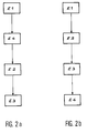
- Figures 2a and 2b each represent a variant of a second embodiment of the method for forming an image according to the invention.
- Bicubic interpolation makes it possible to find a cubic interpolation function for the sampling coordinates x and y of an image I: it preserves the values of the image, of the derivatives first ⁇ I / ⁇ x, ⁇ I / ⁇ y and cross ⁇ 2 I / ⁇ x ⁇ y at the initial sampling points and allow these values to vary continuously at the pixel boundaries.
- the interpolation step bicubic E4 precedes an oversampling step E2.
- This first variant is illustrated in FIG. 2a.
- the bicubic interpolation step E4 allows then to create P1 first intermediate pixels to from each detector pixel and the oversampling step E2 allows to create P2 second pixels intermediaries from each first pixel intermediate, the product PlxP2 being equal to P.
- the bicubic interpolation step is a step Nb ratio interpolation and oversampling step a report interpolation step Ns.
- the interpolation ratios Nb and Ns can be, for example, respectively equal to 6 and 7.
- NbxNs n.
- step E3 of distribution of shots received is carried out after the stage E2.
- the visual impression given by the resulting image is devoid of the effect of pixel border.
- the image formed has a "dive" very close to that obtained by an Anger camera.
- the choice of the respective weights Nb and Ns reports allows to define the report signal to noise of the image formed. Such a choice is a simple and effective means of adjusting the "dive" of the image.
- the interpolation step bicubique follows the randomization step E3. This second variant is illustrated in FIG. 2b.
- step E2 of method of forming an image according to the invention creates N pixels, N being a number less than P.
- the bicubic interpolation step E4 makes it possible to create P3 intermediate pixels from each of the N elementary pixels, the product NxP3 being equal to P.
Landscapes
- Physics & Mathematics (AREA)
- General Physics & Mathematics (AREA)
- Engineering & Computer Science (AREA)
- Theoretical Computer Science (AREA)
- Image Processing (AREA)
- Nuclear Medicine (AREA)
Abstract
Description
- une étape permettant de créer N pixels élémentaires à partir d'un pixel détecteur, N étant un nombre entier inférieur ou égal à P, et
- une étape de répartition aléatoire des coups reçus par chaque pixel détecteur dans les N pixels image qui lui correspondent.
- la figure 1 représente les différentes étapes d'un premier mode de réalisation du procédé de formation d'une image selon l'invention,
- les figures 2a et 2b représentent chacune une variante d'un deuxième mode de réalisation du procédé de formation d'une image selon l'invention.
Claims (10)
- Procédé de formation d'une image (I) obtenue à partir d'un réseau de pixels détecteurs comprenant au moins un pixel détecteur, l'image formée étant constituée d'au moins un ensemble de P pixels image pour chaque pixel détecteur, caractérisé en ce que qu'il comprend successivement :une étape (E2) permettant de créer N pixels élémentaires à partir d'un pixel détecteur, N étant un nombre entier inférieur ou égal à P, et,une étape (E3) de répartition aléatoire des coups reçus par un pixel détecteur dans les N pixels élémentaires qui lui correspondent.
- Procédé selon la revendication 1, caractérisé en ce que l'étape permettant de créer N pixels élémentaires à partir d'un pixel détecteur est une étape de sur-échantillonnage du pixel détecteur de sorte qu'un pixel élémentaire constitue un pixel image (N=P).
- Procédé selon la revendication 1, caractérisé en ce que l'étape (E2) permettant de créer N pixels élémentaires à partir d'un pixel détecteur comprend successivement :une étape d'interpolation (E4) permettant de créer P1 premiers pixels intermédiaires à partir de chaque pixel détecteur et permettant d'atténuer ou de supprimer les limites visibles de chaque pixel détecteur,une étape de sur-échantillonnage (E2) permettant de créer P2 deuxièmes pixels intermédiaires à partir de chaque premier pixel intermédiaire, le produit P1xP2 étant égal à P, de sorte qu'un pixel élémentaire constitue un pixel image (N=P).
- Procédé selon la revendication 3, caractérisé en ce que l'étape d'interpolation (E4) permettant de créer P1 premiers pixels intermédiaires à partir de chaque pixel détecteur et permettant d'atténuer ou de supprimer les limites visibles de chaque pixel détecteur est une étape d'interpolation bicubique.
- Procédé selon la revendication 1, caractérisé en ce qu'il comprend une étape supplémentaire qui succède à l'étape (E3) de répartition aléatoire des coups reçus par un pixel détecteur, l'étape supplémentaire étant une étape d'interpolation (E4) permettant de créer P3 pixels intermédiaires à partir de chacun des N pixels élémentaires et permettant d'atténuer ou de supprimer les limites visibles de chaque pixel détecteur, le produit NxP3 étant égal à P.
- Procédé selon la revendication 5, caractérisé en ce que l'étape d'interpolation (E4) permettant de créer P3 pixels intermédiaires à partir de chacun des N pixels élémentaires et permettant d'atténuer ou de supprimer les limites visibles de chaque pixel détecteur est une étape d'interpolation bicubique.
- Procédé selon l'une quelconque des revendications précédentes, caractérisé en ce que l'étape de répartition aléatoire met en oeuvre la répartition des coups reçus selon une distribution de Poisson.
- Procédé selon l'une quelconque des revendications précédentes, caractérisé en ce que les pixels détecteurs sont des pixels en matériau semi-conducteur CdZnTe ou CdTe.
- Procédé selon l'une quelconque des revendications précédentes, caractérisé en ce qu'un ensemble de P pixels image constitue une matrice carrée de nxn pixels image.
- Procédé selon la revendication 9, caractérisé en ce que n=42.
Applications Claiming Priority (2)
| Application Number | Priority Date | Filing Date | Title |
|---|---|---|---|
| FR9905775A FR2793374B1 (fr) | 1999-05-06 | 1999-05-06 | Procede de formation d'image |
| FR9905775 | 1999-05-06 |
Publications (2)
| Publication Number | Publication Date |
|---|---|
| EP1050763A1 true EP1050763A1 (fr) | 2000-11-08 |
| EP1050763B1 EP1050763B1 (fr) | 2004-03-17 |
Family
ID=9545290
Family Applications (1)
| Application Number | Title | Priority Date | Filing Date |
|---|---|---|---|
| EP00401201A Expired - Lifetime EP1050763B1 (fr) | 1999-05-06 | 2000-05-02 | Procédé de formation d'image |
Country Status (4)
| Country | Link |
|---|---|
| US (1) | US6763147B1 (fr) |
| EP (1) | EP1050763B1 (fr) |
| DE (1) | DE60008958T2 (fr) |
| FR (1) | FR2793374B1 (fr) |
Citations (3)
| Publication number | Priority date | Publication date | Assignee | Title |
|---|---|---|---|---|
| US5491342A (en) * | 1994-11-10 | 1996-02-13 | Trionix Research Laboratory, Inc. | Apparatus and method for nuclear camera calibration |
| US5508524A (en) * | 1994-10-03 | 1996-04-16 | Adac Laboratories, Inc. | Spatially variant PMT cluster constitution and spatially variant PMT weights |
| US5576547A (en) * | 1993-07-27 | 1996-11-19 | Park Medical Systems Inc. | Position calculation and energy correction in the digital scintillation camera |
Family Cites Families (4)
| Publication number | Priority date | Publication date | Assignee | Title |
|---|---|---|---|---|
| FR2546633B1 (fr) * | 1983-05-27 | 1985-07-05 | Thomson Csf | Procede de traitement des impulsions de localisation delivrees par une gammacamera et gammacamera mettant en oeuvre ce procede |
| AU706101B2 (en) * | 1994-12-23 | 1999-06-10 | Digirad | Semiconductor gamma-ray camera and medical imaging system |
| US6025875A (en) * | 1995-10-23 | 2000-02-15 | National Semiconductor Corporation | Analog signal sampler for imaging systems |
| US5847398A (en) * | 1997-07-17 | 1998-12-08 | Imarad Imaging Systems Ltd. | Gamma-ray imaging with sub-pixel resolution |
-
1999
- 1999-05-06 FR FR9905775A patent/FR2793374B1/fr not_active Expired - Fee Related
-
2000
- 2000-04-17 US US09/550,593 patent/US6763147B1/en not_active Expired - Fee Related
- 2000-05-02 DE DE60008958T patent/DE60008958T2/de not_active Expired - Lifetime
- 2000-05-02 EP EP00401201A patent/EP1050763B1/fr not_active Expired - Lifetime
Patent Citations (3)
| Publication number | Priority date | Publication date | Assignee | Title |
|---|---|---|---|---|
| US5576547A (en) * | 1993-07-27 | 1996-11-19 | Park Medical Systems Inc. | Position calculation and energy correction in the digital scintillation camera |
| US5508524A (en) * | 1994-10-03 | 1996-04-16 | Adac Laboratories, Inc. | Spatially variant PMT cluster constitution and spatially variant PMT weights |
| US5491342A (en) * | 1994-11-10 | 1996-02-13 | Trionix Research Laboratory, Inc. | Apparatus and method for nuclear camera calibration |
Also Published As
| Publication number | Publication date |
|---|---|
| FR2793374B1 (fr) | 2001-06-22 |
| EP1050763B1 (fr) | 2004-03-17 |
| DE60008958T2 (de) | 2005-01-27 |
| US6763147B1 (en) | 2004-07-13 |
| DE60008958D1 (de) | 2004-04-22 |
| FR2793374A1 (fr) | 2000-11-10 |
Similar Documents
| Publication | Publication Date | Title |
|---|---|---|
| Magnan | Detection of visible photons in CCD and CMOS: A comparative view | |
| Catrysse et al. | Roadmap for CMOS image sensors: Moore meets Planck and Sommerfeld | |
| FR2537369A1 (fr) | Dispositif analyseur d'image a semi-conducteurs et systeme analyseur l'utilisant | |
| FR2509942A1 (fr) | Camera de television a l'etat solide | |
| EP0977269A1 (fr) | Capteur d'image à réseau de photodiodes | |
| US7990445B2 (en) | Image sensor having differing wavelength filters | |
| FR2593343A1 (fr) | Matrice d'elements photosensibles et son procede de fabrication, procede de lecture associe, et application de cette matrice a la prise de vue d'images | |
| EP1050763B1 (fr) | Procédé de formation d'image | |
| CA2526793C (fr) | Capteur d'image matriciel en technologie cmos | |
| FR2708147A1 (fr) | Capteur d'images à semi-conducteur du type à CCD. | |
| US6628331B1 (en) | Cyan-magenta-yellow-blue color filter array | |
| EP1673932B1 (fr) | Procede de commande d un dispositif photosensible | |
| FR2945667A1 (fr) | Capteur d'image integre a tres grande sensibilite. | |
| US20060186363A1 (en) | Enhanced spectral range imaging sensor | |
| Prest et al. | Improved QE in CMOS image sensors with nano-black antireflection layer | |
| FR2593986A1 (fr) | Systeme de lecture rapide d'un capteur optique matriciel a transfert de charges organise en transfert de trame monocoup pour la detection video d'images breves | |
| FR2666170A1 (fr) | Imageur haute resolution a bas niveau de lumiere. | |
| Ay et al. | CMOS active pixel sensor (APS) imager for scientific applications | |
| FR3011980A1 (fr) | Capteur d'image a multiplication d'electrons et a lecture regroupee de pixels | |
| US5648667A (en) | Image pickup device with and image pickup method by use of two-dimensionally arranged sensors having sensitivities different in certain direction of arrangement | |
| CN108364966A (zh) | 图像传感器及其形成方法 | |
| FR2768554A1 (fr) | Dispositif d'affichage a emission de champ et son procede de commande | |
| FR2513018A1 (fr) | Dispositif semiconducteur de formation d'image couleurs | |
| JPH0759097A (ja) | 多感光領域を有するカラー撮像電荷結合アレイ | |
| Ahrenkiel | The Race to Electronic Photography |
Legal Events
| Date | Code | Title | Description |
|---|---|---|---|
| PUAI | Public reference made under article 153(3) epc to a published international application that has entered the european phase |
Free format text: ORIGINAL CODE: 0009012 |
|
| AK | Designated contracting states |
Kind code of ref document: A1 Designated state(s): DE GB IT |
|
| AX | Request for extension of the european patent |
Free format text: AL;LT;LV;MK;RO;SI |
|
| 17P | Request for examination filed |
Effective date: 20010420 |
|
| AKX | Designation fees paid |
Free format text: DE GB IT |
|
| GRAP | Despatch of communication of intention to grant a patent |
Free format text: ORIGINAL CODE: EPIDOSNIGR1 |
|
| GRAS | Grant fee paid |
Free format text: ORIGINAL CODE: EPIDOSNIGR3 |
|
| GRAA | (expected) grant |
Free format text: ORIGINAL CODE: 0009210 |
|
| AK | Designated contracting states |
Kind code of ref document: B1 Designated state(s): DE GB IT |
|
| REG | Reference to a national code |
Ref country code: GB Ref legal event code: FG4D Free format text: NOT ENGLISH |
|
| REF | Corresponds to: |
Ref document number: 60008958 Country of ref document: DE Date of ref document: 20040422 Kind code of ref document: P |
|
| GBT | Gb: translation of ep patent filed (gb section 77(6)(a)/1977) |
Effective date: 20040614 |
|
| PLBE | No opposition filed within time limit |
Free format text: ORIGINAL CODE: 0009261 |
|
| STAA | Information on the status of an ep patent application or granted ep patent |
Free format text: STATUS: NO OPPOSITION FILED WITHIN TIME LIMIT |
|
| 26N | No opposition filed |
Effective date: 20041220 |
|
| PGFP | Annual fee paid to national office [announced via postgrant information from national office to epo] |
Ref country code: GB Payment date: 20110520 Year of fee payment: 12 |
|
| PGFP | Annual fee paid to national office [announced via postgrant information from national office to epo] |
Ref country code: DE Payment date: 20110520 Year of fee payment: 12 Ref country code: IT Payment date: 20110525 Year of fee payment: 12 |
|
| GBPC | Gb: european patent ceased through non-payment of renewal fee |
Effective date: 20120502 |
|
| PG25 | Lapsed in a contracting state [announced via postgrant information from national office to epo] |
Ref country code: IT Free format text: LAPSE BECAUSE OF NON-PAYMENT OF DUE FEES Effective date: 20120502 |
|
| REG | Reference to a national code |
Ref country code: DE Ref legal event code: R119 Ref document number: 60008958 Country of ref document: DE Effective date: 20121201 |
|
| PG25 | Lapsed in a contracting state [announced via postgrant information from national office to epo] |
Ref country code: GB Free format text: LAPSE BECAUSE OF NON-PAYMENT OF DUE FEES Effective date: 20120502 |
|
| PG25 | Lapsed in a contracting state [announced via postgrant information from national office to epo] |
Ref country code: DE Free format text: LAPSE BECAUSE OF NON-PAYMENT OF DUE FEES Effective date: 20121201 |