EP1049154A2 - Process for forming device isolation region - Google Patents
Process for forming device isolation region Download PDFInfo
- Publication number
- EP1049154A2 EP1049154A2 EP00303599A EP00303599A EP1049154A2 EP 1049154 A2 EP1049154 A2 EP 1049154A2 EP 00303599 A EP00303599 A EP 00303599A EP 00303599 A EP00303599 A EP 00303599A EP 1049154 A2 EP1049154 A2 EP 1049154A2
- Authority
- EP
- European Patent Office
- Prior art keywords
- oxide film
- silicon nitride
- trench
- nitride film
- oxidization
- Prior art date
- Legal status (The legal status is an assumption and is not a legal conclusion. Google has not performed a legal analysis and makes no representation as to the accuracy of the status listed.)
- Granted
Links
Images


Classifications
-
- H—ELECTRICITY
- H10—SEMICONDUCTOR DEVICES; ELECTRIC SOLID-STATE DEVICES NOT OTHERWISE PROVIDED FOR
- H10W—GENERIC PACKAGES, INTERCONNECTIONS, CONNECTORS OR OTHER CONSTRUCTIONAL DETAILS OF DEVICES COVERED BY CLASS H10
- H10W10/00—Isolation regions in semiconductor bodies between components of integrated devices
-
- H—ELECTRICITY
- H10—SEMICONDUCTOR DEVICES; ELECTRIC SOLID-STATE DEVICES NOT OTHERWISE PROVIDED FOR
- H10W—GENERIC PACKAGES, INTERCONNECTIONS, CONNECTORS OR OTHER CONSTRUCTIONAL DETAILS OF DEVICES COVERED BY CLASS H10
- H10W10/00—Isolation regions in semiconductor bodies between components of integrated devices
- H10W10/01—Manufacture or treatment
-
- H—ELECTRICITY
- H10—SEMICONDUCTOR DEVICES; ELECTRIC SOLID-STATE DEVICES NOT OTHERWISE PROVIDED FOR
- H10W—GENERIC PACKAGES, INTERCONNECTIONS, CONNECTORS OR OTHER CONSTRUCTIONAL DETAILS OF DEVICES COVERED BY CLASS H10
- H10W10/00—Isolation regions in semiconductor bodies between components of integrated devices
- H10W10/01—Manufacture or treatment
- H10W10/011—Manufacture or treatment of isolation regions comprising dielectric materials
- H10W10/014—Manufacture or treatment of isolation regions comprising dielectric materials using trench refilling with dielectric materials, e.g. shallow trench isolations
- H10W10/0145—Manufacture or treatment of isolation regions comprising dielectric materials using trench refilling with dielectric materials, e.g. shallow trench isolations of trenches having shapes other than rectangular or V-shape
- H10W10/0147—Manufacture or treatment of isolation regions comprising dielectric materials using trench refilling with dielectric materials, e.g. shallow trench isolations of trenches having shapes other than rectangular or V-shape the shapes being altered by a local oxidation of silicon process, e.g. trench corner rounding by LOCOS
-
- H—ELECTRICITY
- H10—SEMICONDUCTOR DEVICES; ELECTRIC SOLID-STATE DEVICES NOT OTHERWISE PROVIDED FOR
- H10W—GENERIC PACKAGES, INTERCONNECTIONS, CONNECTORS OR OTHER CONSTRUCTIONAL DETAILS OF DEVICES COVERED BY CLASS H10
- H10W10/00—Isolation regions in semiconductor bodies between components of integrated devices
- H10W10/10—Isolation regions comprising dielectric materials
- H10W10/17—Isolation regions comprising dielectric materials formed using trench refilling with dielectric materials, e.g. shallow trench isolations
Definitions
- the present invention relates to a process for forming a device isolation region of a trench structure.
- a pad oxide film 12 of 50 to 200 ⁇ thick and a silicon nitride film 13 of 1000 to 2000 A thick are formed on a silicon substrate 11.
- a resist pattern is formed to cover an active region by a lithography process.
- the silicon nitride film 13 and the pad oxide film 12 in a region for forming a device isolation region are removed by dry etching.
- a trench is formed in the silicon substrate 11 by dry etching as shown in Fig. 5(b).
- the bottom and the sides of the trench formed in the silicon substrate 11 are oxidized by a thickness of 50 to 500 ⁇ at a temperature of 900 to 1100°C.
- a protective film 14 of a silicon oxide film By the oxidization, an opening of the trench in the silicon substrate 11 is rounded and the sides and the bottom of the silicon substrate 11 are covered with a protective film 14 of a silicon oxide film.
- an oxide film 15 is deposited by CVD to completely fill the trench.
- the buried oxide film 15 is flattened by chemical mechanical polishing.
- the silicon nitride film 13 and the pad oxide film 12 are removed as shown in Fig. 6(c).
- a gate oxide film 16 is formed, and a gate electrode material 17 is deposited thereon as seen in Fig. 7(a) and patterned into a gate electrode 17a by lithography and dry etching.
- an edge of the opening of the trench formed in the silicon substrate 11 takes a sharp and almost right-angled form.
- the edge of the trench opening is optimized by oxidizing the edge in a certain oxidizing atmosphere at a certain oxidizing temperature after the formation of the trench so that the edge "a" is rounded.
- the oxidization forms the protective film 14 of a silicon oxide film on the surface of the trench.
- the thickness of the flattened buried oxide film 15 filled in the trench is reduced by removal of the silicon nitride film 13 and the pad oxide film 12.
- a top portion of the buried oxide film in the device isolation region becomes lower than the surface of the silicon substrate in the active region as shown in Fig. 6(c).
- a channel region at a final stage extends to include the edge of the trench opening as shown in Fig. 7(b). Accordingly, if the edge is not sufficiently rounded, a gate electric field strengthens at this portion when a MOS transistor is operated and the transistor assumes apparent characteristics as if parasitic MOS transistors having much lower threshold value arc arranged in parallel. Further, in a non-volatile memory utilizing the gate oxide film 16 as a tunnel oxide film, an F-N tunneling electric field increases in the edge region. Therefore an F-N tunneling current increases locally, and reliability in rewriting the non-volatile memory is deteriorated. Further, a thickness of the gate oxide film is reduced in the region where the edge is not sufficiently rounded, which further accelerates the above problem.
- the optimization of the edge of the trench opening needs to be performed in one oxidization after the trench is formed. Therefore, to oxidize the edge for better roundness, the edge must be oxidized to a greater extent in one time.
- the silicon oxide film formed by oxidizing silicon increases in volume, which causes internal stress to accumulate in the edge region of the trench opening. Therefore, it is problematic because the device characteristics are adversely affected, the profile of the edge is varied due to a remarkable increase of the stress immediately after the oxidization or variations in the profile are increased.
- the present invention is intended to improve flexibility to control the curvature of the edge region of the trench opening provided in the silicon substrate which also serves as an edge portion of an active region, alleviate the stress concentrated on the region and reduce heat hysteresis necessary to obtain a desired profile of the edge region.
- a process for forming a device isolation region comprising the steps of: forming a pad oxide film and a silicon nitride film on a semiconductor substrate; removing the pad oxide film and the silicon nitride film on a region for device isolation and forming a trench in the semiconductor substrate by etching using the remaining pad oxide film and silicon nitride film as an etching mask; forming a first oxide film on the bottom and sidewalls of the trench and below the pad oxide film under an end portion of the silicon nitride film using the silicon nitride film as a mask resistant to oxidization; forming a gap between the silicon nitride film and the semiconductor substrate by removing the first oxide film on the bottom and the sidewalls of the trench and the first oxide film and the pad oxide film below the end portion of the silicon nitride film by etching using the silicon nitride film as an etching mask; forming a second oxide film at least on the bottom and the sidewall
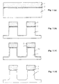
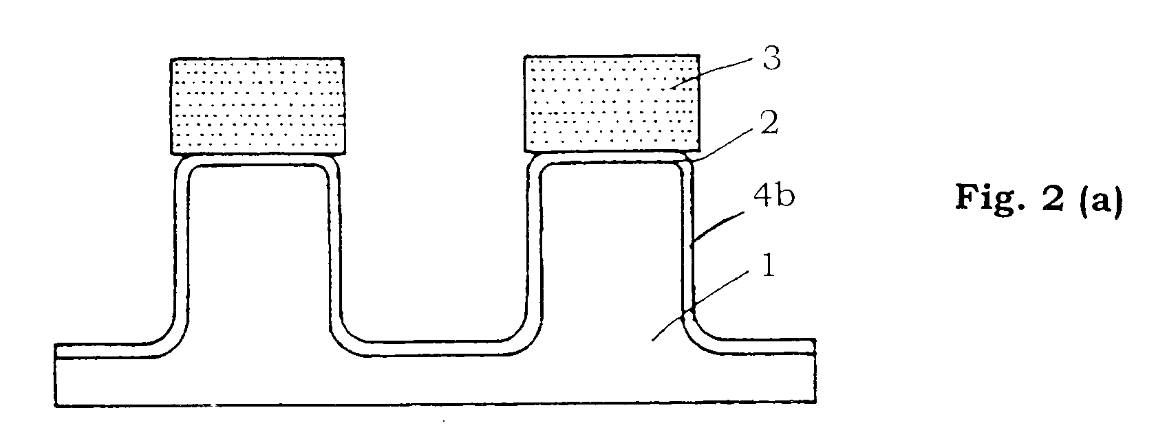
- a pad oxide film 2 of 50 to 200 ⁇ thick and a silicon nitride film 3 of 1000 to 2000 ⁇ thick are formed on a silicon substrate 1.
- the pad oxide film may be formed by a known technique such as thermal oxidization.
- the silicon nitride film may be formed by a known technique such as CVD or sputtering.
- the silicon substrate is used as a semiconductor substrate, but the substrate is not limited thereto.
- a resist pattern (not shown) having an opening in a region for device isolation is formed on the entire surface of the silicon substrate 1 by lithography.
- a trench is formed in the silicon substrate 1, for example, by dry etching using the resist pattern as a mask.
- the depth of the trench is preferably 2000 to 5000 ⁇ .
- a first oxidization is performed to form a first silicon oxide film (a first oxide film) 4a on the sides and the bottom of the trench formed in the silicon substrate 1.
- the obtained silicon oxide film gives greater stress to the circumference thereof than in a second oxidization to be performed later. This is because the silicon substrate 1 and the pad oxide film 2 under the silicon nitride film 3 in an edge region of the trench scarcely have a space therebetween at the first oxidization.
- the first oxidization is desirable to be performed at a low temperature such as 950 °C or low (ex., 400 to 950 °C) so that the stress is suppressed lower.
- the thickness of the resulting first silicon oxide film is desirably thin such as 350 ⁇ (ex., 20 to 500 ⁇ ) so that the stress is suppressed lower. It is needless to say that a portion defined by a top surface of the semiconductor substrate and a side of the trench (hereinafter refereed to as "a corner portion”) is rounded by the first oxidization, but the corner portion is not necessarily rounded to a sufficient extent at this point of time.
- the first silicon oxide film 4a in the trench is removed, for example, by etching with a hydrofluoric acid solution using the silicon nitride film 3 as an etching mask.
- an opening (indicated by "b" in Fig. 4) is formed between the silicon substrate and the end portion of the silicon nitride film in the corner portion.
- Providing the opening is effective in preliminarily eliminating the oxide film which will cause stress in the later second oxidization step. It is also effective in removing defects and contaminants at the sides and the bottom of the trench caused by the etching for forming the trench.
- the above-described etching needs to be performed to such an extent that the silicon substrate at the bottom and the sides of the trench is exposed and the oxide film on the corner portion (the rounded portion in particular) is completely removed. As a result thereof, an end portion of the pad oxide film moves inward from an end portion of the silicon nitride film lying thereon.
- the thickness of the pad oxide film is the same at the end portion and in the neighborhood of the center of the active region.
- the etching is desirably conducted to reduce 25 % or more (ex., 120 to 200 % or more) of the thickness of the oxide film formed by the first oxidization.
- size "c” of the opening "b" becomes larger than the thickness of the pad oxide film.
- the size “c” is preferably larger than the thickness of the pad oxide film by 110 to 200 % of the latter.
- the size "c” is determined according to the thickness of the first oxide film 4a and the oxidization conditions for the first oxide film 4a.
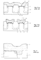
- the corner portion is rounded by the second oxidization using the silicon nitride film as a mask resistant to oxidization and at least the sides and the bottom of the trench are covered with a second silicon oxide film (a second oxide film) 4b. Since the space has been provided between the silicon substrate 1 and the silicon nitride film 3 at the corner portion in the previous step, the space permits the volume expansion of the silicon oxide film grown at the corner portion, which is different from the first oxidization. Therefore, in the second oxidization, the stress due to the volume expansion of the oxide film between the silicon substrate and the silicon nitride film at the corner portion is reduced as compared with the first oxidization. Further, since the opening has been previously provided, an oxidization seed is easily supplied to the corner portion so that the corner portion can be effectively rounded.
- the stress accumulated on the corner portion is restrained to an extent similar to that in the conventional oxidization.
- the stress is more reduced.
- the oxidization temperature in the first oxidization is preferably 950 °C or low and the thickness of the resulting first silicon oxide film is preferably 350 ⁇ or less.
- the second oxidization is preferably performed at a temperature similar to or higher than that for the first oxidization within a range of 900 to 1100 °C.
- the thickness of the second silicon oxide film is preferably similar to or larger than that of the first silicon oxide film within a range of 50 to 500 ⁇ .
- the second oxidization is intended to round the corner portion. Therefore, the second oxidization is preferably performed at about 1100 °C at which viscosity of silicon at a high temperature can be utilized.
- the second oxidization is preferably performed at 950 °C or low. More specifically, where the first oxidization is performed at 920 °C to form the first silicon oxide film of 250 ⁇ thick, the second oxidization may be performed at 1100 °C to form the second silicon oxide film of 350 ⁇ thick. Further, where the first oxidization is performed at 920 °C to form the first silicon oxide film of 250 ⁇ thick, the second oxidization may be performed at 920 °C to form the second silicon oxide film of 350 ⁇ thick.
- a silicon oxide film (a third oxide film) 5 is deposited, for example, by CVD to fill the trench so that a device isolation region is formed.
- the silicon oxide film 5 is flattened by subjecting it to chemical mechanical polishing.
- the pad oxide film 2 and the silicon nitride film 3 are removed to complete the formation of the active region and the device isolation region.
- a gate oxide film 6 and an electrode material 7 of polysilicon or the like arc deposited and patterned by a known technique to form a gate electrode 7a.
- a corner portion of a desired round shape can be obtained while suppressing both stress accumulated on the corner portion and heat hysteresis smaller.
- the suppression of the stress and the heat hysteresis allows preventing generation of defects of silicon, stabilizing the shape of the corner portion, thereby to realize high reliability of semiconductor devices and non-volatile memories as well as high accuracy of threshold value distribution.
- the stress and the heat hysteresis have the same level as the conventional ones, the round corner portion having greater curvature can be obtained.
- an oxide film containing contaminants and defects is entirely removed from a trench formed in a substrate, a silicon substrate with high quality can be prepared.
Landscapes
- Element Separation (AREA)
- Semiconductor Memories (AREA)
- Non-Volatile Memory (AREA)
- Local Oxidation Of Silicon (AREA)
Abstract


Description
Claims (7)
- A process for forming a device isolation region comprising the steps of:forming a pad oxide film and a silicon nitride film on a semiconductor substrate;removing the pad oxide film and the silicon nitride film on a region for device isolation and forming a trench in the semiconductor substrate by etching using the remaining pad oxide film and silicon nitride film as an etching mask;forming a first oxide film at least on the bottom and sidewalls of the trench and below the pad oxide film under an end portion of the silicon nitride film using the silicon nitride film as a mask resistant to oxidization;forming a gap between the silicon nitride film and the semiconductor substrate by removing the first oxide film on the bottom and the sidewalls of the trench and the first oxide film and the pad oxide film below the end portion of the silicon nitride film by etching using the silicon nitride film as an etching mask;forming a second oxide film at least on the bottom and the sidewalls of the trench and in the gap using the silicon nitride film as a mask resistant to oxidization; andforming a third oxide film so as to fill the trench, thereby to form a device isolation region.
- A process according to claim 1, wherein the second oxide film is thicker than the first oxide film.
- A process according to claim 2, wherein the first oxide film has a thickness of 20 to 500 Å and the second oxide film has a thickness of 50 to 500 Å.
- A process according to claim 1, wherein the second oxide film is formed at a temperature higher than a temperature for forming the first oxide film.
- A process according to claim 4, wherein the first oxide film is formed at 400 to 950 °C and the second oxide film is formed at 900 to 1100 °C.
- A process according to claim 1, wherein the first oxide film between the silicon nitride film and the semiconductor substrate is removed toward a width direction of the semiconductor substrate from the end portion of the silicon nitride film by 120 to 200 % or more of the thickness of the first oxide film on the sidewalls of the trench.
- A process according to claim 1, wherein the gap between the end portion of the silicon nitride film and the semiconductor substrate is formed larger than the pad oxide film by 110 to 200 % of the latter in a depth direction of the semiconductor substrate.
Applications Claiming Priority (2)
| Application Number | Priority Date | Filing Date | Title |
|---|---|---|---|
| JP12109599A JP3566880B2 (en) | 1999-04-28 | 1999-04-28 | Method of forming element isolation region |
| JP12109599 | 1999-04-28 |
Publications (3)
| Publication Number | Publication Date |
|---|---|
| EP1049154A2 true EP1049154A2 (en) | 2000-11-02 |
| EP1049154A3 EP1049154A3 (en) | 2002-12-18 |
| EP1049154B1 EP1049154B1 (en) | 2006-02-15 |
Family
ID=14802763
Family Applications (1)
| Application Number | Title | Priority Date | Filing Date |
|---|---|---|---|
| EP00303599A Expired - Lifetime EP1049154B1 (en) | 1999-04-28 | 2000-04-28 | Process for forming device isolation region |
Country Status (6)
| Country | Link |
|---|---|
| US (1) | US6323107B1 (en) |
| EP (1) | EP1049154B1 (en) |
| JP (1) | JP3566880B2 (en) |
| KR (1) | KR100367051B1 (en) |
| DE (1) | DE60025991T2 (en) |
| TW (1) | TW473907B (en) |
Cited By (1)
| Publication number | Priority date | Publication date | Assignee | Title |
|---|---|---|---|---|
| WO2003043078A3 (en) * | 2001-11-13 | 2003-11-06 | Advanced Micro Devices Inc | Preferential corner rounding of trench structures using post-fill oxidation |
Families Citing this family (18)
| Publication number | Priority date | Publication date | Assignee | Title |
|---|---|---|---|---|
| US7289174B1 (en) | 1995-07-17 | 2007-10-30 | Seiko Epson Corporation | Reflective type color liquid crystal device and an electronic apparatus using this |
| JP3702162B2 (en) * | 2000-09-25 | 2005-10-05 | 三洋電機株式会社 | Manufacturing method of semiconductor device |
| JP2003100860A (en) | 2001-09-27 | 2003-04-04 | Toshiba Corp | Semiconductor device |
| KR100426485B1 (en) * | 2001-12-22 | 2004-04-14 | 주식회사 하이닉스반도체 | Method of manufacturing a flash memory cell |
| US7439141B2 (en) * | 2001-12-27 | 2008-10-21 | Spansion, Llc | Shallow trench isolation approach for improved STI corner rounding |
| US6890831B2 (en) * | 2002-06-03 | 2005-05-10 | Sanyo Electric Co., Ltd. | Method of fabricating semiconductor device |
| KR100466189B1 (en) * | 2002-06-04 | 2005-01-13 | 주식회사 하이닉스반도체 | Method of manufacturing a flash memory cell |
| KR100475081B1 (en) * | 2002-07-09 | 2005-03-10 | 삼성전자주식회사 | SONOS type EEPROM and method for fabricating the same |
| JP2004095886A (en) * | 2002-08-30 | 2004-03-25 | Fujitsu Ltd | Semiconductor device and manufacturing method thereof |
| US20040065937A1 (en) * | 2002-10-07 | 2004-04-08 | Chia-Shun Hsiao | Floating gate memory structures and fabrication methods |
| KR100843244B1 (en) * | 2007-04-19 | 2008-07-02 | 삼성전자주식회사 | Semiconductor device and manufacturing method thereof |
| US7812375B2 (en) * | 2003-05-28 | 2010-10-12 | Samsung Electronics Co., Ltd. | Non-volatile memory device and method of fabricating the same |
| KR100719366B1 (en) * | 2005-06-15 | 2007-05-17 | 삼성전자주식회사 | Method of forming a semiconductor device having a trench isolation film |
| US20070262963A1 (en) * | 2006-05-11 | 2007-11-15 | Cypress Semiconductor Corporation | Apparatus and method for recognizing a button operation on a sensing device |
| JP2008103420A (en) * | 2006-10-17 | 2008-05-01 | Elpida Memory Inc | Manufacturing method of semiconductor device |
| US9006079B2 (en) * | 2012-10-19 | 2015-04-14 | Taiwan Semiconductor Manufacturing Company, Ltd. | Methods for forming semiconductor fins with reduced widths |
| CN107026192B (en) * | 2016-02-02 | 2020-05-29 | 中芯国际集成电路制造(上海)有限公司 | Method for manufacturing semiconductor device |
| CN113517296B (en) * | 2020-04-10 | 2025-02-07 | 合肥晶合集成电路股份有限公司 | A non-volatile memory structure and preparation method thereof |
Family Cites Families (9)
| Publication number | Priority date | Publication date | Assignee | Title |
|---|---|---|---|---|
| US5258332A (en) * | 1987-08-28 | 1993-11-02 | Kabushiki Kaisha Toshiba | Method of manufacturing semiconductor devices including rounding of corner portions by etching |
| KR970053470A (en) * | 1995-12-29 | 1997-07-31 | 김주용 | Device Separation Method of Semiconductor Device |
| JP3414590B2 (en) * | 1996-06-20 | 2003-06-09 | 株式会社東芝 | Method for manufacturing semiconductor device |
| US5834358A (en) * | 1996-11-12 | 1998-11-10 | Micron Technology, Inc. | Isolation regions and methods of forming isolation regions |
| US5863827A (en) * | 1997-06-03 | 1999-01-26 | Texas Instruments Incorporated | Oxide deglaze before sidewall oxidation of mesa or trench |
| US5880004A (en) * | 1997-06-10 | 1999-03-09 | Winbond Electronics Corp. | Trench isolation process |
| US6103635A (en) * | 1997-10-28 | 2000-08-15 | Fairchild Semiconductor Corp. | Trench forming process and integrated circuit device including a trench |
| US6054343A (en) * | 1998-01-26 | 2000-04-25 | Texas Instruments Incorporated | Nitride trench fill process for increasing shallow trench isolation (STI) robustness |
| US6074932A (en) * | 1998-01-28 | 2000-06-13 | Texas Instruments - Acer Incorporated | Method for forming a stress-free shallow trench isolation |
-
1999
- 1999-04-28 JP JP12109599A patent/JP3566880B2/en not_active Expired - Fee Related
-
2000
- 2000-04-11 US US09/547,105 patent/US6323107B1/en not_active Expired - Fee Related
- 2000-04-13 TW TW089106881A patent/TW473907B/en not_active IP Right Cessation
- 2000-04-26 KR KR10-2000-0022121A patent/KR100367051B1/en not_active Expired - Fee Related
- 2000-04-28 EP EP00303599A patent/EP1049154B1/en not_active Expired - Lifetime
- 2000-04-28 DE DE60025991T patent/DE60025991T2/en not_active Expired - Lifetime
Cited By (1)
| Publication number | Priority date | Publication date | Assignee | Title |
|---|---|---|---|---|
| WO2003043078A3 (en) * | 2001-11-13 | 2003-11-06 | Advanced Micro Devices Inc | Preferential corner rounding of trench structures using post-fill oxidation |
Also Published As
| Publication number | Publication date |
|---|---|
| US6323107B1 (en) | 2001-11-27 |
| DE60025991T2 (en) | 2006-10-19 |
| KR20000071817A (en) | 2000-11-25 |
| JP2000311938A (en) | 2000-11-07 |
| EP1049154A3 (en) | 2002-12-18 |
| JP3566880B2 (en) | 2004-09-15 |
| EP1049154B1 (en) | 2006-02-15 |
| TW473907B (en) | 2002-01-21 |
| DE60025991D1 (en) | 2006-04-20 |
| KR100367051B1 (en) | 2003-01-09 |
Similar Documents
| Publication | Publication Date | Title |
|---|---|---|
| US6323107B1 (en) | Process for forming device isolation region | |
| US6699773B2 (en) | Shallow trench isolation type semiconductor device and method of forming the same | |
| US5578518A (en) | Method of manufacturing a trench isolation having round corners | |
| US7745904B2 (en) | Shallow trench isolation structure for semiconductor device | |
| US6465866B2 (en) | Trench isolation regions having trench liners with recessed ends | |
| US6995447B2 (en) | Silicon on insulator device having trench isolation layer and method for manufacturing the same | |
| US4373965A (en) | Suppression of parasitic sidewall transistors in locos structures | |
| US5358893A (en) | Isolation method for semiconductor device | |
| KR19990084786A (en) | Trench element isolation | |
| US5472906A (en) | Method of forming isolation | |
| US5512509A (en) | Method for forming an isolation layer in a semiconductor device | |
| US6682986B2 (en) | Method of forming shallow trench isolation and method of manufacturing a semiconductor device using the same | |
| US5972776A (en) | Method of forming a planar isolation structure in an integrated circuit | |
| US5137843A (en) | Isolation method for semiconductor device | |
| US8026133B2 (en) | Method of fabricating a semiconductor device with a non-uniform gate insulating film | |
| US20020160579A1 (en) | Method of manufacturing semiconductor device having shallow trench isolation (STI) | |
| US7485534B2 (en) | Method of manufacture of a trench-gate semiconductor device | |
| US20030082862A1 (en) | Method for fabricating a gate layer stack for an integrated circuit configuration | |
| US20020111046A1 (en) | Semiconductor device fabricating method | |
| US6333242B1 (en) | Method of fabricating semiconductor device without having grooves at edge portions of STI | |
| US20070243681A1 (en) | Method of fabricating flash memory device using sidewall process | |
| JPH07183513A (en) | Method for manufacturing semiconductor device | |
| US7898025B2 (en) | Semiconductor device having recess gate | |
| US7304344B1 (en) | Integrated circuit having independently formed array and peripheral isolation dielectrics | |
| US6444539B1 (en) | Method for producing a shallow trench isolation filled with thermal oxide |
Legal Events
| Date | Code | Title | Description |
|---|---|---|---|
| PUAI | Public reference made under article 153(3) epc to a published international application that has entered the european phase |
Free format text: ORIGINAL CODE: 0009012 |
|
| AK | Designated contracting states |
Kind code of ref document: A2 Designated state(s): AT BE CH CY DE DK ES FI FR GB GR IE IT LI LU MC NL PT SE |
|
| AX | Request for extension of the european patent |
Free format text: AL;LT;LV;MK;RO;SI |
|
| PUAL | Search report despatched |
Free format text: ORIGINAL CODE: 0009013 |
|
| AK | Designated contracting states |
Kind code of ref document: A3 Designated state(s): AT BE CH CY DE DK ES FI FR GB GR IE IT LI LU MC NL PT SE |
|
| AX | Request for extension of the european patent |
Free format text: AL;LT;LV;MK;RO;SI |
|
| 17P | Request for examination filed |
Effective date: 20030226 |
|
| 17Q | First examination report despatched |
Effective date: 20030725 |
|
| AKX | Designation fees paid |
Designated state(s): DE FR GB |
|
| GRAP | Despatch of communication of intention to grant a patent |
Free format text: ORIGINAL CODE: EPIDOSNIGR1 |
|
| GRAS | Grant fee paid |
Free format text: ORIGINAL CODE: EPIDOSNIGR3 |
|
| GRAA | (expected) grant |
Free format text: ORIGINAL CODE: 0009210 |
|
| AK | Designated contracting states |
Kind code of ref document: B1 Designated state(s): DE FR GB |
|
| REG | Reference to a national code |
Ref country code: GB Ref legal event code: FG4D |
|
| REF | Corresponds to: |
Ref document number: 60025991 Country of ref document: DE Date of ref document: 20060420 Kind code of ref document: P |
|
| ET | Fr: translation filed | ||
| PLBE | No opposition filed within time limit |
Free format text: ORIGINAL CODE: 0009261 |
|
| STAA | Information on the status of an ep patent application or granted ep patent |
Free format text: STATUS: NO OPPOSITION FILED WITHIN TIME LIMIT |
|
| 26N | No opposition filed |
Effective date: 20061116 |
|
| PGFP | Annual fee paid to national office [announced via postgrant information from national office to epo] |
Ref country code: GB Payment date: 20130424 Year of fee payment: 14 Ref country code: DE Payment date: 20130508 Year of fee payment: 14 |
|
| PGFP | Annual fee paid to national office [announced via postgrant information from national office to epo] |
Ref country code: FR Payment date: 20130625 Year of fee payment: 14 |
|
| REG | Reference to a national code |
Ref country code: DE Ref legal event code: R119 Ref document number: 60025991 Country of ref document: DE |
|
| GBPC | Gb: european patent ceased through non-payment of renewal fee |
Effective date: 20140428 |
|
| REG | Reference to a national code |
Ref country code: FR Ref legal event code: ST Effective date: 20141231 |
|
| PG25 | Lapsed in a contracting state [announced via postgrant information from national office to epo] |
Ref country code: DE Free format text: LAPSE BECAUSE OF NON-PAYMENT OF DUE FEES Effective date: 20141101 Ref country code: GB Free format text: LAPSE BECAUSE OF NON-PAYMENT OF DUE FEES Effective date: 20140428 |
|
| REG | Reference to a national code |
Ref country code: DE Ref legal event code: R119 Ref document number: 60025991 Country of ref document: DE Effective date: 20141101 |
|
| PG25 | Lapsed in a contracting state [announced via postgrant information from national office to epo] |
Ref country code: FR Free format text: LAPSE BECAUSE OF NON-PAYMENT OF DUE FEES Effective date: 20140430 |