EP1049110A2 - Large area thick film resistors with improved predictability and uniformity and method for producing same - Google Patents
Large area thick film resistors with improved predictability and uniformity and method for producing same Download PDFInfo
- Publication number
- EP1049110A2 EP1049110A2 EP00100840A EP00100840A EP1049110A2 EP 1049110 A2 EP1049110 A2 EP 1049110A2 EP 00100840 A EP00100840 A EP 00100840A EP 00100840 A EP00100840 A EP 00100840A EP 1049110 A2 EP1049110 A2 EP 1049110A2
- Authority
- EP
- European Patent Office
- Prior art keywords
- resistor
- emulsion
- large area
- thick film
- film resistors
- Prior art date
- Legal status (The legal status is an assumption and is not a legal conclusion. Google has not performed a legal analysis and makes no representation as to the accuracy of the status listed.)
- Granted
Links
Images


Classifications
-
- H—ELECTRICITY
- H01—ELECTRIC ELEMENTS
- H01C—RESISTORS
- H01C17/00—Apparatus or processes specially adapted for manufacturing resistors
- H01C17/06—Apparatus or processes specially adapted for manufacturing resistors adapted for coating resistive material on a base
- H01C17/065—Apparatus or processes specially adapted for manufacturing resistors adapted for coating resistive material on a base by thick film techniques, e.g. serigraphy
-
- H—ELECTRICITY
- H05—ELECTRIC TECHNIQUES NOT OTHERWISE PROVIDED FOR
- H05K—PRINTED CIRCUITS; CASINGS OR CONSTRUCTIONAL DETAILS OF ELECTRIC APPARATUS; MANUFACTURE OF ASSEMBLAGES OF ELECTRICAL COMPONENTS
- H05K1/00—Printed circuits
- H05K1/16—Printed circuits incorporating printed electric components, e.g. printed resistors, capacitors or inductors
- H05K1/167—Printed circuits incorporating printed electric components, e.g. printed resistors, capacitors or inductors incorporating printed resistors
-
- H—ELECTRICITY
- H05—ELECTRIC TECHNIQUES NOT OTHERWISE PROVIDED FOR
- H05K—PRINTED CIRCUITS; CASINGS OR CONSTRUCTIONAL DETAILS OF ELECTRIC APPARATUS; MANUFACTURE OF ASSEMBLAGES OF ELECTRICAL COMPONENTS
- H05K3/00—Apparatus or processes for manufacturing printed circuits
- H05K3/10—Apparatus or processes for manufacturing printed circuits in which conductive material is applied to the insulating support in such a manner as to form the desired conductive pattern
- H05K3/12—Apparatus or processes for manufacturing printed circuits in which conductive material is applied to the insulating support in such a manner as to form the desired conductive pattern using thick film techniques, e.g. printing techniques to apply the conductive material or similar techniques for applying conductive paste or ink patterns
- H05K3/1216—Apparatus or processes for manufacturing printed circuits in which conductive material is applied to the insulating support in such a manner as to form the desired conductive pattern using thick film techniques, e.g. printing techniques to apply the conductive material or similar techniques for applying conductive paste or ink patterns by screen printing or stencil printing
- H05K3/1233—Methods or means for supplying the conductive material and for forcing it through the screen or stencil
Definitions
- the present invention relates generally to microcircuits and more particularly to large area thick film resistors.
- Hybrid circuitry generally uses thick film resistors with geometries greater than 30 mils. Other applications of hybrid circuitry and other circuitry may use smaller resistors which provide for a more cost-effective circuit since less area on the ceramic is used.
- the present invention provides large area, thick film resistors with improved predictability and uniformity and method for producing same.
- "Tent poles" are employed during the printing of the large area resistors to prop up the screen mesh to ensure the resultant resistor does not have a scooped out center portion.
- FIG. 1a shows a side view of a representative first step in printing a small resistor.
- An emulsion 120 is disposed upon a substrate 110.
- the substrate 110 can be, for example, 96% alumina.
- Screen wire 130 is disposed upon the emulsion paste 120.
- the distance between the emulsion 120 print is x 1 , where x 1 is less than 40 mils wide.
- a squeegee 140 is moved across the screen 130 and emulsion 120, leaving the resistor 150 (in FIG. 1c).
- the thickness of the small resistor 150 is determined by the thickness of the mesh 130 and emulsion 120.
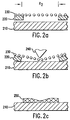
- the distance x 2 is greater than 40 mils wide.
- the mesh 230 Since there is a large span between emulsion prints 220, the only thing supporting the squeegee 240 as it is passed across the material is the mesh 230.
- the resistor 250 that results has a scooped-out middle section. This is commonly referred to as "screen sag.” That is, the thickness at the edges of the large resistor 250 is determined by the thickness of the emulsion 220 and the mesh 230, the thickness of the center portion of the large resistor 250 is determined by the mesh thickness only.
- the large resistor 250 will print thin, resulting in a higher sheet resistance than a comparable aspect-ratio small resistor (see FIG. 1). And, since the large resistor 250 tends to print too thin, the resultant resistor value may be larger than was required. A laser trim cannot solve this overshoot problem since common laser trimming techniques only trim resistance up (i.e., resistance increases).
- a tent pole made of gold 362 is used.
- the technique is to print small gold pads in the interior of the resistor (i.e., between the emulsion 320 prints).
- the gold pads can be printed at the same time as printing the conductors.
- the advantage of this technique is that it is easy and there are no extra prints.
- a tent pole made of resistor 364 is used.
- the technique is to print a small resistor spot in the interior of the resistor (i.e., between the emulsion 320 prints).
- the resistor spot must be printed prior to printing the large resistor.
- the spot 364 should be small, for example, less than 10 x 10 mils.
- the advantage of this technique is that it uses a uniform material and it's extendable (i.e., can print several dry resistor spots on the same area to add height to the tent pole).
- a tent pole made of emulsion 366 is used.
- the technique is to print a small emulsion spot in the interior of the resistor (i.e., between the emulsion 320 prints).
- the emulsion spot can be printed at the same time the other emulsion print is printed.
- the spot 364 should be small, for example, less than 10 x 10 mils.
- the advantage of this technique is that it is self leveling (i.e., spots are exactly the same thickness as the emulsion at the end of the resistor).
Landscapes
- Engineering & Computer Science (AREA)
- Manufacturing & Machinery (AREA)
- Microelectronics & Electronic Packaging (AREA)
- Manufacturing Of Printed Wiring (AREA)
- Apparatuses And Processes For Manufacturing Resistors (AREA)
- Parts Printed On Printed Circuit Boards (AREA)
Abstract
Description
Claims (4)
- A method for printing a large area resistor (150) comprising the steps of:(1) printing an emulsion (120) on a substrate (110), the emulsion print having a void (x1) of predetermined width;(2) placing a tent pole (362, 364, 366) in the void;(3) laying down a screen mesh (330) above the emulsion and tent pole;(4) using a squeegee (140) to finish the print.
- The method of claim 1 wherein the tent pole is a gold pad (362).
- The method of claim 1 wherein the tent pole is a resistor spot (364).
- The method of claim 1 wherein the tent pole is an emulsion spot (366).
Applications Claiming Priority (2)
| Application Number | Priority Date | Filing Date | Title |
|---|---|---|---|
| US09/301,898 US6187372B1 (en) | 1999-04-29 | 1999-04-29 | Method for producing large area thick film resistors with uniform thickness |
| US301898 | 1999-04-29 |
Publications (3)
| Publication Number | Publication Date |
|---|---|
| EP1049110A2 true EP1049110A2 (en) | 2000-11-02 |
| EP1049110A3 EP1049110A3 (en) | 2003-10-15 |
| EP1049110B1 EP1049110B1 (en) | 2005-05-04 |
Family
ID=23165361
Family Applications (1)
| Application Number | Title | Priority Date | Filing Date |
|---|---|---|---|
| EP00100840A Expired - Lifetime EP1049110B1 (en) | 1999-04-29 | 2000-01-17 | Large area thick film resistors with improved predictability and uniformity and method for producing same |
Country Status (4)
| Country | Link |
|---|---|
| US (1) | US6187372B1 (en) |
| EP (1) | EP1049110B1 (en) |
| JP (1) | JP2000353609A (en) |
| DE (1) | DE60019842T2 (en) |
Families Citing this family (4)
| Publication number | Priority date | Publication date | Assignee | Title |
|---|---|---|---|---|
| EP1567302B8 (en) * | 2002-11-21 | 2013-05-15 | Hadco Santa Clara, Inc. | Laser trimming of resistors |
| US7297896B2 (en) * | 2002-11-21 | 2007-11-20 | Hadco Santa Clara, Inc. | Laser trimming of resistors |
| US6972391B2 (en) * | 2002-11-21 | 2005-12-06 | Hadco Santa Clara, Inc. | Laser trimming of annular passive components |
| TWI370464B (en) * | 2007-04-19 | 2012-08-11 | Ind Tech Res Inst | Resistance layout structure and manufacture method thereof |
Family Cites Families (4)
| Publication number | Priority date | Publication date | Assignee | Title |
|---|---|---|---|---|
| US4183136A (en) * | 1977-08-03 | 1980-01-15 | Johnson Controls, Inc. | Temperature sensing resistance device |
| US4242401A (en) * | 1978-01-24 | 1980-12-30 | Mitani Electronics Industry Corp. | Screen-printing mask |
| US4338351A (en) * | 1980-09-10 | 1982-07-06 | Cts Corporation | Apparatus and method for producing uniform fired resistors |
| GB8705075D0 (en) * | 1987-03-04 | 1987-04-08 | Pilkington Brothers Plc | Printing |
-
1999
- 1999-04-29 US US09/301,898 patent/US6187372B1/en not_active Expired - Fee Related
-
2000
- 2000-01-17 DE DE60019842T patent/DE60019842T2/en not_active Expired - Fee Related
- 2000-01-17 EP EP00100840A patent/EP1049110B1/en not_active Expired - Lifetime
- 2000-04-27 JP JP2000127874A patent/JP2000353609A/en active Pending
Also Published As
| Publication number | Publication date |
|---|---|
| JP2000353609A (en) | 2000-12-19 |
| DE60019842T2 (en) | 2006-04-27 |
| DE60019842D1 (en) | 2005-06-09 |
| EP1049110A3 (en) | 2003-10-15 |
| US6187372B1 (en) | 2001-02-13 |
| EP1049110B1 (en) | 2005-05-04 |
Similar Documents
| Publication | Publication Date | Title |
|---|---|---|
| US4678531A (en) | Method and apparatus for screen printing solder paste onto a substrate with device premounted thereon | |
| US6352026B1 (en) | Screen printing apparatus for printing layers having different thicknesses | |
| JPH0524231A (en) | Thermal head and electronic equipment using the same | |
| US6187372B1 (en) | Method for producing large area thick film resistors with uniform thickness | |
| EP0347824B1 (en) | A thick film forming process | |
| US20040075520A1 (en) | Strip conductor having an additional layer in a curved section | |
| JPS59215763A (en) | Printer for thick film | |
| JP2002059534A (en) | Screen printing method and screen printing machine | |
| JPH0364094A (en) | Conductive layer pattern forming equipment on green sheets | |
| JPH06340103A (en) | Thermal head | |
| JPH03281391A (en) | Screen for electronic device | |
| JPH10313153A (en) | Printed board | |
| JPH1134473A (en) | Pattern printing method | |
| JPS58159301A (en) | printed resistance device | |
| JPH02312203A (en) | Method of trimming thick film resistor | |
| JP2000340345A (en) | Heating body | |
| JPH03185789A (en) | Formation of electric circuit | |
| JPH08139381A (en) | Method for forming electrodes of piezoelectric transformer | |
| JPH03114756A (en) | Heating element | |
| JP2001102715A (en) | Parts structure for conductive adhesive | |
| JPH0837355A (en) | Thick film resistance element | |
| JPH05135918A (en) | Indication forming part of resistor | |
| JPS59152876A (en) | Thermal head apparatus | |
| JPH0714668U (en) | Circuit board device | |
| JPH07304198A (en) | Thermal print head and manufacturing method thereof |
Legal Events
| Date | Code | Title | Description |
|---|---|---|---|
| PUAI | Public reference made under article 153(3) epc to a published international application that has entered the european phase |
Free format text: ORIGINAL CODE: 0009012 |
|
| AK | Designated contracting states |
Kind code of ref document: A2 Designated state(s): AT BE CH CY DE DK ES FI FR GB GR IE IT LI LU MC NL PT SE |
|
| AX | Request for extension of the european patent |
Free format text: AL;LT;LV;MK;RO;SI |
|
| RAP1 | Party data changed (applicant data changed or rights of an application transferred) |
Owner name: AGILENT TECHNOLOGIES INC |
|
| RAP1 | Party data changed (applicant data changed or rights of an application transferred) |
Owner name: AGILENT TECHNOLOGIES INC. |
|
| RAP1 | Party data changed (applicant data changed or rights of an application transferred) |
Owner name: AGILENT TECHNOLOGIES INC. A DELAWARE CORPORATION |
|
| RAP1 | Party data changed (applicant data changed or rights of an application transferred) |
Owner name: AGILENT TECHNOLOGIES, INC. (A DELAWARE CORPORATION |
|
| PUAL | Search report despatched |
Free format text: ORIGINAL CODE: 0009013 |
|
| AK | Designated contracting states |
Kind code of ref document: A3 Designated state(s): AT BE CH CY DE DK ES FI FR GB GR IE IT LI LU MC NL PT SE |
|
| AX | Request for extension of the european patent |
Extension state: AL LT LV MK RO SI |
|
| RIC1 | Information provided on ipc code assigned before grant |
Ipc: 7H 01C 17/065 A |
|
| 17P | Request for examination filed |
Effective date: 20031024 |
|
| AKX | Designation fees paid |
Designated state(s): DE GB |
|
| GRAP | Despatch of communication of intention to grant a patent |
Free format text: ORIGINAL CODE: EPIDOSNIGR1 |
|
| GRAS | Grant fee paid |
Free format text: ORIGINAL CODE: EPIDOSNIGR3 |
|
| GRAA | (expected) grant |
Free format text: ORIGINAL CODE: 0009210 |
|
| AK | Designated contracting states |
Kind code of ref document: B1 Designated state(s): DE GB |
|
| REG | Reference to a national code |
Ref country code: GB Ref legal event code: FG4D |
|
| REG | Reference to a national code |
Ref country code: IE Ref legal event code: FG4D |
|
| REF | Corresponds to: |
Ref document number: 60019842 Country of ref document: DE Date of ref document: 20050609 Kind code of ref document: P |
|
| PGFP | Annual fee paid to national office [announced via postgrant information from national office to epo] |
Ref country code: DE Payment date: 20060228 Year of fee payment: 7 |
|
| PLBE | No opposition filed within time limit |
Free format text: ORIGINAL CODE: 0009261 |
|
| STAA | Information on the status of an ep patent application or granted ep patent |
Free format text: STATUS: NO OPPOSITION FILED WITHIN TIME LIMIT |
|
| 26N | No opposition filed |
Effective date: 20060207 |
|
| PG25 | Lapsed in a contracting state [announced via postgrant information from national office to epo] |
Ref country code: DE Free format text: LAPSE BECAUSE OF NON-PAYMENT OF DUE FEES Effective date: 20070801 |
|
| GBPC | Gb: european patent ceased through non-payment of renewal fee |
Effective date: 20070117 |
|
| PG25 | Lapsed in a contracting state [announced via postgrant information from national office to epo] |
Ref country code: GB Free format text: LAPSE BECAUSE OF NON-PAYMENT OF DUE FEES Effective date: 20070117 |
|
| PGFP | Annual fee paid to national office [announced via postgrant information from national office to epo] |
Ref country code: GB Payment date: 20060113 Year of fee payment: 7 |