EP1049023A2 - Device and method for controlling data packet transfer - Google Patents
Device and method for controlling data packet transfer Download PDFInfo
- Publication number
- EP1049023A2 EP1049023A2 EP00302271A EP00302271A EP1049023A2 EP 1049023 A2 EP1049023 A2 EP 1049023A2 EP 00302271 A EP00302271 A EP 00302271A EP 00302271 A EP00302271 A EP 00302271A EP 1049023 A2 EP1049023 A2 EP 1049023A2
- Authority
- EP
- European Patent Office
- Prior art keywords
- data
- transfer
- packets
- initialization
- nodes
- Prior art date
- Legal status (The legal status is an assumption and is not a legal conclusion. Google has not performed a legal analysis and makes no representation as to the accuracy of the status listed.)
- Granted
Links
Images


Classifications
-
- H—ELECTRICITY
- H04—ELECTRIC COMMUNICATION TECHNIQUE
- H04L—TRANSMISSION OF DIGITAL INFORMATION, e.g. TELEGRAPHIC COMMUNICATION
- H04L12/00—Data switching networks
- H04L12/28—Data switching networks characterised by path configuration, e.g. LAN [Local Area Networks] or WAN [Wide Area Networks]
- H04L12/40—Bus networks
- H04L12/40052—High-speed IEEE 1394 serial bus
- H04L12/40058—Isochronous transmission
-
- H—ELECTRICITY
- H04—ELECTRIC COMMUNICATION TECHNIQUE
- H04L—TRANSMISSION OF DIGITAL INFORMATION, e.g. TELEGRAPHIC COMMUNICATION
- H04L12/00—Data switching networks
- H04L12/28—Data switching networks characterised by path configuration, e.g. LAN [Local Area Networks] or WAN [Wide Area Networks]
- H04L12/40—Bus networks
- H04L12/40052—High-speed IEEE 1394 serial bus
- H04L12/40117—Interconnection of audio or video/imaging devices
-
- H—ELECTRICITY
- H04—ELECTRIC COMMUNICATION TECHNIQUE
- H04L—TRANSMISSION OF DIGITAL INFORMATION, e.g. TELEGRAPHIC COMMUNICATION
- H04L9/00—Cryptographic mechanisms or cryptographic arrangements for secret or secure communications; Network security protocols
- H04L9/40—Network security protocols
-
- H—ELECTRICITY
- H04—ELECTRIC COMMUNICATION TECHNIQUE
- H04L—TRANSMISSION OF DIGITAL INFORMATION, e.g. TELEGRAPHIC COMMUNICATION
- H04L69/00—Network arrangements, protocols or services independent of the application payload and not provided for in the other groups of this subclass
- H04L69/30—Definitions, standards or architectural aspects of layered protocol stacks
- H04L69/32—Architecture of open systems interconnection [OSI] 7-layer type protocol stacks, e.g. the interfaces between the data link level and the physical level
- H04L69/322—Intralayer communication protocols among peer entities or protocol data unit [PDU] definitions
- H04L69/324—Intralayer communication protocols among peer entities or protocol data unit [PDU] definitions in the data link layer [OSI layer 2], e.g. HDLC
Definitions
- the present invention relates to a device and a method for controlling packet transfer, and for example, to a packet transfer controller that complies with the IEEE 1394 interface standard.
- the IEEE 1394 standard is used in controllers that transfer large and continuous amounts of data, such as dynamic image data, at high speeds.
- isochronous data transfer is performed every 125 ⁇ s.
- An irregularity in the transfer timing of the dynamic image data results in insufficient continuity of the reproduced dynamic image. This causes the reproduced dynamic image to lack reality.
- isochronous transfer is performed by dividing the dynamic image data into a plurality of packets and continuously transferring the packets at equal intervals. This allows the reproduced dynamic image to look real.
- Hot plugging is standardized by the IEEE 1394 and refers to the connection or disconnection of one or more devices (nodes) to an IEEE 1394 bus while power is being supplied to the bus. Further, hot plugging results in topology changes.
- a prior art transfer controller When the topology changes, a prior art transfer controller performs initialization or bus reset to map the topology even while packets are being transferred.
- the initialization interrupts the transfer of packets and interferes with the reproduction of real looking dynamic images (i.e.., smooth motion video ).
- a packet transfer device used to transfer data between a plurality of nodes.
- the packet transfer device includes a processor for storing a series of data in a plurality of packets.
- the series of data is divided into a plurality of blocks, each stored in one of the packets.
- the packets are transferred at equal intervals.
- An initialization prohibition unit prohibits initialization of the nodes during the transfer of the data.
- Another aspect of the present invention provides a packet transfer method for transferring a series of data between a plurality of nodes.
- the method includes the steps of dividing the series of data, storing the divided data in a plurality of packets, sequentially transferring the packets at equal intervals, and prohibiting initialization of the nodes during the transfer of the packets.
- a further aspect of the present invention provides a packet transfer controller for controlling the transfer of a series of data packets between nodes connected to each other by a bus cable.
- the nodes and the bus cable define a bus topology.
- the controller includes a socket for mating with a plug of the bus cable. When the plug mates with the socket, the bus cable is electrically connected to the controller.
- a processing circuit connected to the socket, transmits packets to and receives packets from the bus cable.
- a host processor is connected to the processing circuit to receive packets therefrom and transmitting packets thereto.
- a monitor circuit monitors the transfer of the series of data packets between the nodes. While a series of packets is being transferred between the nodes, the monitoring circuit inhibits reinitialization caused by changing the bus topology.
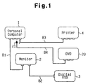
- the computer system illustrated in Fig. 1 uses IEEE 1394 compatible bus cables B1-B4.
- the bus cable B1 connects a monitor 2 to a personal computer 1.
- the bus cable B2 connects a digital VTR 3 to the monitor 2.
- the bus cable B3 connects a printer 4 to the computer 1.
- the bus cable B4 is connected to a DVD device 23, but not connected to the computer 1.
- Fig. 2 is a schematic block diagram showing a packet transfer controller 11, which is incorporated in the computer 1.
- the monitor 2, the digital VTR 3, and the printer 4 are each also provided with the same packet transfer controller 11.
- the packet transfer controller 11 includes a socket 12, a physical layer processing circuit 13, a link layer processing circuit 14, a monitoring circuit 15, a host processor 16, a comparator 17, a register 18, a lock mechanism 19, and an indicator 20.
- the socket 12 is connected to the physical layer processing circuit 13.
- the physical layer processing circuit 13 is connected to the link layer processing circuit 14.
- the link layer processing circuit 14 is connected to the monitoring circuit 15.
- the monitoring circuit 15 is connected to the host processor 16.
- the host processor 16 is connected to the comparator 17 and the register 18.
- the register 18 is connected to the comparator 17.
- the comparator 17 is connected to the monitoring circuit 15, the lock mechanism 19, and the indicator 20.
- the socket 12 is connected to a plug 21 of the bus cable B1.
- the computer 1 includes a number of sockets 12 which correspond to the number of ports of the node (computer 1). As shown in Fig. 1, the computer 1 is provided with four of the sockets 12.
- Packets transferred from other nodes are provided to the physical layer processing circuit 13 via the socket 12.
- the physical layer processing circuit 13 converts the electrical signals of each packet to logic signals and provides the logic signals to the link layer processing circuit 14.
- the physical layer processing circuit 13 also converts logic signals from the link layer processing circuit 14 and converts them to electrical signals that are transferred to other nodes via the cable B1.
- the link layer processing circuit 14 checks the format of the input packet. During the format check, the link layer processing circuit 14 determines whether the packet is addressed to its node from the contents of a header, which is included in the packet. If the packet is addressed to its node, the link layer processing circuit 14 passes the packet through the monitoring circuit 15 to the host processor 16.
- the host processor 16 divides the data into a plurality of blocks. Each block is stored in a packet, which is generated by the host processor 16. The packets are provided to the link layer processing circuit 14 at equal intervals (125 ⁇ s).
- the host processor 16 has a cycle timer register (CTR) 22.
- the CTR 22 is provided with a timer (not shown) to measure time.
- the host processor 16 outputs the packets at equal intervals based on the measured time. Further, the host processor 16 computes the time length required for the completion of isochronous data transfer based on the data amount. The host processor 16 then calculates the completion time of the isochronous data transfer using the time measured by the CTR 22 and stores the completion time information in the register 18.
- CTR cycle timer register
- the comparator 17 detects the completion of the isochronous data transfer, or the timing for cancelling topology lock cancellation timing, upon completion of the isochronous data transfer.
- the comparator 17 compares the data transfer completion time stored in the register 18 with the current time kept by the CTR 22. If the time kept by the CTR 22 has not reached the transfer completion time, the comparator 17 provides a lock signal R to the monitoring circuit 15, the lock mechanism 19, and the indicator 20. If the time kept by the CTR 22 has reached the transfer completion time, the comparator 17 provides an unlock signal /R to the monitoring circuit 15, the lock mechanism 19, and the indicator 20.
- the monitoring circuit 15 monitors the signals received from the host processor 16 when activated in response to the lock signal R.
- the unlock signal /R deactivates the monitoring circuit 15 and prevents it from monitoring the signals from the host processor 16. More specifically, when the host processor 16 provides an initialization signal to the physical layer processing circuit 13, the monitoring circuit 15, when activated, inhibits the signal, and when deactivated, permits all of the command signals from the upstream devices to be provided to the physical layer processing circuit 13.
- the initialization signal is a command generated by the host processor 16 or a device upstream of the host processor 16. Upon receipt of the command, the physical layer processing circuit 13 begins initialization, or bus reset, to map the new topology created by adding a new node.
- the lock mechanism 19 When activated by the lock signal R, the lock mechanism 19 physically prohibits connection of the plug 21 to the socket 12 and disconnection of the plug 21 from the socket 12 (hot plugging).
- the unlock signal /R deactivates the lock mechanism 19 so that connection of the plug 21 to the socket 12 and disconnection of the plug 21 from the socket 12 (hot plugging) is permitted.
- the indicator 20 includes an LED lamp arranged near the socket 12. The indicator 20 is lit in response to the lock signal R to indicate that data is being transferred and turned off in response to the unlock signal /R to indicate that data is not being transferred.
- the comparator 17, the monitoring circuit 15, the lock mechanism 19, the indicator 20, and the CTR 22 form an initialization prohibition unit.
- the packet transfer controller 11 where the isochronous packet originates, performs steps S1-S14, which are illustrated in Figs. 3 and 4.
- the host processor 16 computes the length of time required to complete the transfer of the data packets.
- step S2 the host processor 16 determines whether the lock signal R is being output by the comparator 17. If the lock signal R is not being output, the host processor 16 proceeds to step S3.
- the host processor 16 adds the time length obtained in step S1 to the, time measured by the CTR 22 and provides the sum to the register 18.
- the sum is also contained in packets provided to the link layer processing circuit 14 by the host processor 16.
- the completion time of the data transfer is stored in the register 18 of the packet transfer controller 11 and in the registers 18 of packet transfer controllers 11 incorporated in other nodes.
- the data transfer completion time is stored in a start request packet of a cycle start packet (CS packet).
- the start request packet stores information used to transmit the CS packet to a root node.
- the root node that receives the information transmits the CS packet to each node at equal intervals (125 ⁇ s).
- the comparator 17 provides the lock signal R to the monitoring circuit 15, the lock mechanism 19, and the indicator 20 when the time value of the CTR 22 is smiler than that stored in the register 18. This activates the monitoring circuit 15. In this state, the monitoring circuit 15 monitors the signals sent to the link layer processing circuit 14 from the host processor 16. The indicator 20 is lit in response to the lock signal R to indicate that data is being isochronously transferred. The lock signal R also activates the lock mechanism 19. This prohibits changes in the connection state of the socket 12 and the plug 21. Thus, the topology is maintained and bus reset is prohibited.
- step S2 if the lock signal R is active, that is, if data is already being isochronously transferred between nodes, the host processor 16 proceeds to step S5.
- step S5 the host processor 16 recalculates the time value of the register 18 since the value obtained in step S1 is greater than the time value of the register 18 indicating that the isochronous transfer time still has to be extended. More specifically, the host processor 16 adds the time length obtained in step S1 to the time of the CTR 22 and updates the transfer completion time stored in the register 18 with the obtained value.
- the host processor 16 provides the updated value in a renewed request packet to the link layer processing circuit 14.
- step S6 the comparator 17 determines whether the time value stored in the register 18 is greater than the time value of the CTR 22. If the time value of the CTR 22 is equal to or less than the time value of the register 18, the host processor 16 proceeds to step S7.
- the packet transfer controller 11 performs a packet transfer process. More specifically, the host processor 16 transmits packets to the link layer processing circuit 14 in response to the CS packet and receives packets from other nodes. After the packet transfer process is completed, the host processor 16 proceeds to step S8.
- step S8 the host processor 16 determines whether a received packet is a renewed request packet. If the packet is a renewed request packet, the host processor 16 proceeds to step S9.
- the host processor 16 adds the time value of the renewed request packet to the time value of the CTR 22 to update the transfer completion time stored in the register 18.
- the monitoring circuit 15 determines whether the host processor 16 is providing an initialization command signal to the physical layer processing circuit 13. If the initialization command signal is being provided, the host processor 16 proceeds to step S11. At step S11, the monitoring circuit 15 inhibits the initialization command signal. The host processor 16 then returns to step S6. If the initialization command signal is not being provided in step S10, the host processor 16 returns to step S6. This prevents bus reset.
- step S6 If the comparator 17 determines that the time value stored in the register 18 is greater than that of the CTR 22 in step S6, the host processor 16 proceeds to step S12.
- the comparator 17 outputs the unlock signal /R.
- the indicator 20 is turned off and the lock mechanism 19 is deactivated. This permits changes in the connection state of the plug 21 and the socket 12.
- the deactivated monitoring circuit 15 determines whether the initialization command signal has been inhibited in step S11. If the initialization command signal is being held, the host processor 16 proceeds to step S14. At step S14, the monitoring circuit 15 provides the initialization command signal to the link layer processing circuit 14. This starts the initialization process, after the completion of isochronous transfer.
- the host processor 16 When the host processor 16 receives packets of image data or the like at equal intervals, the host processor 16, the comparator 17, and the monitoring circuit 15 perform steps S21, S22, and S6-S14, which are illustrated in Figs- 4 and 5.
- the host processor 16 refers to the start request packet of the CS packet and adds the time length required to complete the transfer of data to the time of the CTR 22 and provides the sum to the register 18.
- the register 18 of the node that receives packets stores the completion time of the data packet transfer.
- the comparator 17 provides the lock signal R to the monitoring circuit 15, the lock mechanism 19, and the indicator 20 (since the time value of the CTR 22 is smaller than that of the register 18).
- the lock mechanism 19 In response to the lock signal R, the lock mechanism 19 physically prohibits hot plugging of the plug 21 relative to the socket 12. This prevents bus reset, which is caused by hot plugging.
- the indicator 20 is lit in response to the lock signal R to indicate that data is being transferred isochronously.
- the host processor 16 then proceeds to step S6 and performs steps S6-S14.
- the digital VTR 3 isochronously transfers a series of data (image data) to the computer 1.
- the host processor 16 of the packet transfer controller 11 incorporated in the digital VTR 3 receives a command signal, which enables data transfer to the computer 1, from an upstream circuit. Then, the host processor 16 divides the series of data into a plurality of blocks and stores each block in a packet.
- the host processor 16 computes the time required to transfer all of the packets.
- step S2 the host processor 16 determines that the lock signal R is not being output.
- the host processor 16 adds the time length to the time of the CTR 22 and stores the sum in the register 18.
- the obtained data transfer completion time is stored in the start request packet of a CS packet and transmitted to the nodes 1, 2, 4.
- the time value of the CTR 22 is smaller than the time value of the register 18.
- the comparator 17 provides the lock signal R to the monitoring circuit 15, the lock mechanism 19, and the indicator 20. This activates the monitoring circuit 15 and lights the indicator 20.
- the lock mechanism 19 prohibits the connection state of the socket 12 and the plug 21 of the bus cables B1-B3 from being changed. In this state, referring to Fig. 1, the bus cable B4 extending from the DVD device 23 cannot be connected to the socket 12 of the computer 1. Further, the plug 21 of the bus cable B3, which connects the printer 4 and the computer 1, cannot be disconnected from the socket 12 of the computer 1. Thus, the bus topology is maintained.
- one of the data packets is transmitted to the link layer processing circuit 14 from the host processor 16.
- the transmitted packet passes through the link layer processing circuit 14 and the physical layer processing circuit 13 and is output from the packet transfer controller 11 of the digital VTR 3.
- the packet is then transmitted to the packet transfer controller 11 of the computer 1 via the bus cables B2, B1.
- Steps S6 to S11 are repeated until the comparator 17 determines that the time value of the CTR 22 is greater than that of the register 18 in step S6.
- step S7 is repeated until the transmission of all of the packets, in which the divided series of data are stored, is completed.
- step S9 When a renewed request packet is received from the other nodes 1, 3, 4 while step S7 is being repeated, the time value of the register 18 is updated to a value obtained by adding the time value of the CTR 22 to the time value of the renewed request packet (step S9). If an initialization command signal is received by the monitoring circuit 15 when step S7 is being repeated, the monitoring circuit 15 inhibits the command signal (step S11).
- the time value of the CTR 22 becomes greater than that of the register 18 upon completion of the data transfer.
- the comparator 17 provides the unlock signal /R to the monitoring circuit 15, the lock mechanism 19, and the indicator 20. This deactivates the lock mechanism 19 and turns off the indicator 20.
- the lock mechanism 19 permits the connection state of the socket 12 and the plug 21 to be changed. This allows changes in the bus topology.
- the monitoring circuit 15 now provides the command signal to the link layer processing circuit 14 (step S14).
- the link layer processing circuit 14 then provides the initialization command signal to the physical layer processing circuit 13 to perform initialization after completion of the isochronous transfer.
- the monitor 2 isochronously transfers a series of data (image data) to the computer 1 when packet transfer is being performed between the computer 1 and the printer 4.
- the comparator 17 of the printer 4 since data is being isochronously transferred, the comparator 17 of the printer 4 is already outputting the lock signal R. Thus, the monitoring circuit 15 is activated and the indicator 20 is lit. Further, the lock mechanism 19 prevents the bus topology from being changed.
- the host processor 16 of the digital VTR 3 computes the time required to transfer the series of data.
- the host processor 16 determines whether the lock signal R is being output.
- the host processor 16 updates the value of the register 18. The updated data transfer completion time is stored in a renewed request packet and transmitted to each of the nodes 1, 2, 4.
- one of the packets is transmitted to the link layer processing circuit 14 from the host processor 16 of the digital VTR 3 in response to the CS packet.
- the transmitted packet is transmitted from the link layer processing circuit 14 to the physical layer processing circuit 13 and is then transferred to the packet transfer controller 11 of the computer 1 via the bus cables B2, B1. Afterward, data is isochronously transferred between each of the nodes 1-4.
- the transfer time of the first packet and the transfer time of the last packet may be provided to the other nodes 1, 2, 4. Initialization is also prohibited when packets are being transferred.
- Initialization may be prohibited when the CS packet is being transferred, and the initialization may be performed when the CS packet has not transferred for more than a predetermined time.
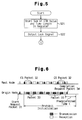
- a start request packet 31 of a CS packet is transmitted from an origin node, or a node where the data to be transferred originates.
- the root node transmits the CS packet 33 at equal intervals.
- the origin node transmits a completion request packet 34 of the CS packet in response to the next CS packet 32 after the transfer of the final packet 33 is completed.
- the root node receives the packet 34, the transmission of the CS packet 32 is stopped.
- the initialization of each of the nodes is permitted.
- This embodiment also has the advantages (1) to (3) of the first embodiment. Further, all of the nodes acknowledge the completion of data transfer without using special packets.
- one or more of the following operations are performed when data is being transferred, (a) maintaining the bus topology, (b) inhibiting the initialization command signal from the host processor 16, and (c) turning the LED lamp on.
- the lock mechanism 19 may be eliminated and replaced by a known connector having hooks to prevent the disconnection of the plug. In this case, if the plug 21 is connected to the socket 12 during the isochronous transfer of data, initialization is prevented if the connector is not electrically connected to the physical layer processing circuit 13.
- the indicator 20 may be arranged at other locations and devices other than the LED may be used as the indicator.
- part of the monitor 2 may be used to indicate that data is being transferred.
- the CTR 22 may be provided in the link layer processing circuit 14.
- the time length may be stored in a packet other than the start request packet of the CS packet and provided to the other nodes.
- the monitoring circuit 15 may be arranged between the link layer processing circuit 14 and the physical layer processing circuit 13.
Landscapes
- Engineering & Computer Science (AREA)
- Computer Networks & Wireless Communication (AREA)
- Signal Processing (AREA)
- Computer Security & Cryptography (AREA)
- Multimedia (AREA)
- Small-Scale Networks (AREA)
- Communication Control (AREA)
- Data Exchanges In Wide-Area Networks (AREA)
Abstract
Description
Claims (18)
- A packet transfer device (11) used to transfer data between a plurality of nodes (1, 2, 3, 4, 23), the packet transfer device including a processor (16) for storing a series of data in a plurality of packets, wherein the series of data is divided into a plurality of blocks, each stored in one of the packets, and wherein the packets are transferred at equal intervals, characterized byan initialization prohibition unit (15, 17, 18, 19, 20, 22) for prohibiting initialization of the nodes during the transfer of the data.
- The device according to claim 1, wherein a bus cable (B1, B2, B3, B4) is connected to the packet transfer device, the device characterized in that the initialization prohibition unit includes a lock mechanism (19) for prohibiting the disconnection of the bus cable during the transfer of data.
- The device according to claims 1 or 2, characterized in that the initialization prohibition unit includes an indicator (20) that indicates when data is being transferred.
- The device according to claims 1, 2 or 3, wherein the processor generates a logic data signal and an initialization command signal, the packet transfer device further characterized by a physical layer processing circuit (13) for receiving the logic data signal and the initialization command signal, and a monitoring circuit (15) that monitors the initialization command signal transmitted to the physical layer processing circuit from the processor.
- The device according to claim 4, characterized in that the monitoring circuit inhibits the transmission of the initialization command signal to the physical layer processing circuit while data is being transferred.
- The device according to claim 5, characterized in that the monitoring circuit transmits the inhibited command signal after completion of the transfer of the series of data.
- The device according to claims 4,5 or 6, charcterized in that the processor computes the length of time required to transfer the series of data and notifies each of the nodes of said time length, and wherein the initialization prohibition unit inhibits the initialization command signal for the computed time length.
- The device according to claim 7, characterized in that the processor uses the computed time length to compute the time at which the transfer of data is completed, and wherein the initialization prohibition unit includes:a register (17) connected to the processor for storing the data transfer completion time;a cycle time register (22) for storing the current time; anda comparator (17) connected to the register and the cycle time register, wherein the comparator compares the current time of the cycle time register with the data transfer completion time of the register and generates a lock signal for inhibiting the initialization command signal in accordance with the comparison result.
- The device according to claims 7 or 8, characterized in that the transfer of data is performed isochronously and includes the transfer of a cycle start packet, wherein the initialization prohibition unit prohibits the initialization in accordance with the cycle start packet and permits the initialization a predetermined time after the cycle start packet has been transferred.
- A packet transfer method for transferring a series of data between a plurality of nodes, the method characterized by the steps of:dividing the series of data;storing the divided data in a plurality of packets;sequentially transferring the packets at equal intervals; andprohibiting initialization of the nodes during the transfer of the packets.
- The method according to claim 10, further comprising the steps of:computing the time length required to transfer all of the packets;notifying each of the nodes of the computed time length; andprohibiting the initialization of the nodes for the computed time length.
- The method according to claim 11, further characterized by the step of inhibiting an initialization command generated by one of the nodes during the computed time length.
- The method according to claims 10,11 or 12, further characterized by the step of permitting initialization subsequent to the packet transfer step.
- A packet transfer controller (11) for controlling the transfer of a series of data packets between nodes (1, 2, 3, 4, 23) connected to each other by a bus cable (B1, B2, B3, B4), wherein the nodes and the bus cable define a bus topology, the controller characterized by:a socket (12) for mating with a plug (21) of the bus cable, wherein when the plug mates with the socket, the bus cable is electrically connected to the controller;a processing circuit (13), connected to the socket, for transmitting packets to and receiving packets from the bus cable;a host processor (16) connected to the processing circuit for receiving packets therefrom and transmitting packets thereto; anda monitor circuit (15) for monitoring the transfer of the series of data packets between the nodes, wherein while a series of packets is being transferred between the nodes, the monitoring circuit inhibits reinitialization caused by changing the bus topology.
- The packet transfer controller of claim 14, wherein the monitor circuit generates a lock signal when the series of packets is being transferred between the nodes, the controller further characterized by:a lock mechanism (19) connected to the socket and the monitor circuit and receiving the lock signal from the monitor circuit, wherein when the lock signal is active, the lock mechanism prevents the plug from being disconnected from the socket.
- The packet transfer controller of claim 14, wherein the monitor circuit generates a lock signal when the series of packets is being transferred between the nodes, the controller further characterized by:an indicator (20) connected to the monitor circuit and receiving the lock signal from the monitor circuit, wherein when the lock signal is active, the indicator is activated, thereby notifying a user that the series of packets is being transferred and that the plug should not be disconnected from the socket.
- The packet transfer controller of claim 16, characterized in that the indicator comprises an LED.
- The packet transfer controller of claim 16, further characterized by:a lock mechanism (19) connected to the socket and the monitor circuit and receiving the lock signal from the monitor circuit, wherein when the lock signal is active, the lock mechanism prevents the plug from being disconnected from the socket.
Applications Claiming Priority (2)
| Application Number | Priority Date | Filing Date | Title |
|---|---|---|---|
| JP11915899 | 1999-04-27 | ||
| JP11915899A JP4237865B2 (en) | 1999-04-27 | 1999-04-27 | Packet transfer control apparatus and method |
Publications (3)
| Publication Number | Publication Date |
|---|---|
| EP1049023A2 true EP1049023A2 (en) | 2000-11-02 |
| EP1049023A3 EP1049023A3 (en) | 2004-06-23 |
| EP1049023B1 EP1049023B1 (en) | 2006-10-11 |
Family
ID=14754366
Family Applications (1)
| Application Number | Title | Priority Date | Filing Date |
|---|---|---|---|
| EP20000302271 Expired - Lifetime EP1049023B1 (en) | 1999-04-27 | 2000-03-21 | Device and method for controlling data packet transfer |
Country Status (5)
| Country | Link |
|---|---|
| US (1) | US6598096B1 (en) |
| EP (1) | EP1049023B1 (en) |
| JP (1) | JP4237865B2 (en) |
| DE (1) | DE60031194T2 (en) |
| TW (1) | TW457789B (en) |
Cited By (1)
| Publication number | Priority date | Publication date | Assignee | Title |
|---|---|---|---|---|
| CN1313940C (en) * | 2003-07-15 | 2007-05-02 | 明基电通股份有限公司 | Method for transmitting display data |
Families Citing this family (4)
| Publication number | Priority date | Publication date | Assignee | Title |
|---|---|---|---|---|
| US7631313B2 (en) * | 2002-06-17 | 2009-12-08 | David Mayhew | System and method for transferring data |
| JP5919729B2 (en) * | 2011-10-27 | 2016-05-18 | セイコーエプソン株式会社 | Peripheral device status monitoring method, device driver and network system |
| US10649418B2 (en) | 2013-12-11 | 2020-05-12 | Ademco Inc. | Building automation controller with configurable audio/visual cues |
| CN104317685A (en) * | 2014-10-14 | 2015-01-28 | 英业达科技有限公司 | Starting method of calculator system |
Family Cites Families (11)
| Publication number | Priority date | Publication date | Assignee | Title |
|---|---|---|---|---|
| US4398230A (en) * | 1980-09-23 | 1983-08-09 | Souriau & Cie. | Protection device for electrical connectors |
| US4517641A (en) * | 1982-04-30 | 1985-05-14 | International Business Machines Corporation | Lookahead I/O device control subsystem |
| US5335325A (en) * | 1987-12-22 | 1994-08-02 | Kendall Square Research Corporation | High-speed packet switching apparatus and method |
| US5461720A (en) * | 1992-09-23 | 1995-10-24 | International Business Machines Corporation | System for increasing the efficiency of communications between controller and plurality of host computers by prohibiting retransmission of the same message for predetermined period of time |
| US5519877A (en) * | 1993-01-12 | 1996-05-21 | Matsushita Electric Industrial Co., Ltd. | Apparatus for synchronizing parallel processing among a plurality of processors |
| JP3249334B2 (en) * | 1995-04-06 | 2002-01-21 | 株式会社東芝 | Digital interface device and digital interface method |
| US6081852A (en) * | 1996-04-26 | 2000-06-27 | Texas Instruments Incorporated | Packet data transferring system for autonomously operating a DMA by autonomous boot mode select signal wherein the DMA is enabled to at least one program control list |
| JPH09331342A (en) | 1996-06-11 | 1997-12-22 | Toshiba Corp | Bus state management device |
| DE69837356T2 (en) * | 1997-02-14 | 2007-11-29 | Canon K.K. | Apparatus, system and method for data transmission and apparatus for image processing |
| WO2000003519A1 (en) * | 1998-07-09 | 2000-01-20 | Sony Corporation | Communication control method, communication system, and electronic device |
| US6202103B1 (en) * | 1998-11-23 | 2001-03-13 | 3A International, Inc. | Bus data analyzer including a modular bus interface |
-
1999
- 1999-04-27 JP JP11915899A patent/JP4237865B2/en not_active Expired - Fee Related
-
2000
- 2000-03-14 TW TW89104618A patent/TW457789B/en not_active IP Right Cessation
- 2000-03-16 US US09/526,750 patent/US6598096B1/en not_active Expired - Lifetime
- 2000-03-21 DE DE2000631194 patent/DE60031194T2/en not_active Expired - Lifetime
- 2000-03-21 EP EP20000302271 patent/EP1049023B1/en not_active Expired - Lifetime
Cited By (1)
| Publication number | Priority date | Publication date | Assignee | Title |
|---|---|---|---|---|
| CN1313940C (en) * | 2003-07-15 | 2007-05-02 | 明基电通股份有限公司 | Method for transmitting display data |
Also Published As
| Publication number | Publication date |
|---|---|
| DE60031194D1 (en) | 2006-11-23 |
| JP2000312214A (en) | 2000-11-07 |
| US6598096B1 (en) | 2003-07-22 |
| TW457789B (en) | 2001-10-01 |
| EP1049023A3 (en) | 2004-06-23 |
| DE60031194T2 (en) | 2007-02-15 |
| JP4237865B2 (en) | 2009-03-11 |
| EP1049023B1 (en) | 2006-10-11 |
Similar Documents
| Publication | Publication Date | Title |
|---|---|---|
| US5764896A (en) | Method and system for reducing transfer latency when transferring data from a network to a computer system | |
| US7401213B2 (en) | Data communication apparatus and method of a device that supports plural communication methods | |
| JP4124873B2 (en) | Power control system | |
| KR19990072918A (en) | Data communication system, data communication method, and data communication apparatus | |
| JPH10243327A (en) | Image input device, control method thereof, and image input / output system | |
| CN1190834A (en) | Communication method and electronic device using the method | |
| US6412076B1 (en) | Signal processing apparatus and image sensing apparatus | |
| KR100407095B1 (en) | Data communication system and data communication method | |
| EP1282265A2 (en) | Media converter and transmission system using the same | |
| EP1049023B1 (en) | Device and method for controlling data packet transfer | |
| JP3630971B2 (en) | Data communication method, apparatus, system, and storage medium | |
| JP3599048B2 (en) | Data transfer control system, electronic device, program, and data transfer control method | |
| US7203787B2 (en) | Information processing apparatus and method that utilizes stored information about a mountable device | |
| US6732262B1 (en) | Method and system for controlling reset of IEEE 1394 network | |
| US20100142562A1 (en) | Interface apparatus and resynchronization method | |
| US20020019868A1 (en) | Method of constructing network topology and interface circuit | |
| US7233592B1 (en) | Packet transfer control circuit | |
| JP4377033B2 (en) | Data transfer control method and apparatus | |
| US7397574B1 (en) | Image processing controlling distribution of work among apparatuses based on apparatus performance | |
| EP1487164A2 (en) | Communication apparatus, method, program and recording medium, where the legality of a disconnection request is judged | |
| US20060017811A1 (en) | Communication system, electronic apparatus, control apparatus, and computer-readable storage medium | |
| CN112685346B (en) | Multi-device data synchronization method based on ARINC429 bus | |
| JP3495879B2 (en) | Data processing method, data processing device, and computer-readable recording medium | |
| JP3495878B2 (en) | Data processing method, data processing device and printer | |
| JP2715137B2 (en) | Communication network control method |
Legal Events
| Date | Code | Title | Description |
|---|---|---|---|
| PUAI | Public reference made under article 153(3) epc to a published international application that has entered the european phase |
Free format text: ORIGINAL CODE: 0009012 |
|
| AK | Designated contracting states |
Kind code of ref document: A2 Designated state(s): AT BE CH CY DE DK ES FI FR GB GR IE IT LI LU MC NL PT SE |
|
| AX | Request for extension of the european patent |
Free format text: AL;LT;LV;MK;RO;SI |
|
| PUAL | Search report despatched |
Free format text: ORIGINAL CODE: 0009013 |
|
| AK | Designated contracting states |
Kind code of ref document: A3 Designated state(s): AT BE CH CY DE DK ES FI FR GB GR IE IT LI LU MC NL PT SE |
|
| AX | Request for extension of the european patent |
Extension state: AL LT LV MK RO SI |
|
| 17P | Request for examination filed |
Effective date: 20041215 |
|
| AKX | Designation fees paid |
Designated state(s): DE FR GB |
|
| 17Q | First examination report despatched |
Effective date: 20050503 |
|
| GRAP | Despatch of communication of intention to grant a patent |
Free format text: ORIGINAL CODE: EPIDOSNIGR1 |
|
| GRAS | Grant fee paid |
Free format text: ORIGINAL CODE: EPIDOSNIGR3 |
|
| GRAA | (expected) grant |
Free format text: ORIGINAL CODE: 0009210 |
|
| AK | Designated contracting states |
Kind code of ref document: B1 Designated state(s): DE FR GB |
|
| REG | Reference to a national code |
Ref country code: GB Ref legal event code: FG4D |
|
| REF | Corresponds to: |
Ref document number: 60031194 Country of ref document: DE Date of ref document: 20061123 Kind code of ref document: P |
|
| ET | Fr: translation filed | ||
| PLBE | No opposition filed within time limit |
Free format text: ORIGINAL CODE: 0009261 |
|
| STAA | Information on the status of an ep patent application or granted ep patent |
Free format text: STATUS: NO OPPOSITION FILED WITHIN TIME LIMIT |
|
| 26N | No opposition filed |
Effective date: 20070712 |
|
| REG | Reference to a national code |
Ref country code: GB Ref legal event code: 732E |
|
| REG | Reference to a national code |
Ref country code: FR Ref legal event code: TP |
|
| PGFP | Annual fee paid to national office [announced via postgrant information from national office to epo] |
Ref country code: GB Payment date: 20090318 Year of fee payment: 10 |
|
| PGFP | Annual fee paid to national office [announced via postgrant information from national office to epo] |
Ref country code: FR Payment date: 20090316 Year of fee payment: 10 |
|
| GBPC | Gb: european patent ceased through non-payment of renewal fee |
Effective date: 20100321 |
|
| REG | Reference to a national code |
Ref country code: FR Ref legal event code: ST Effective date: 20101130 |
|
| PG25 | Lapsed in a contracting state [announced via postgrant information from national office to epo] |
Ref country code: FR Free format text: LAPSE BECAUSE OF NON-PAYMENT OF DUE FEES Effective date: 20100331 |
|
| PG25 | Lapsed in a contracting state [announced via postgrant information from national office to epo] |
Ref country code: GB Free format text: LAPSE BECAUSE OF NON-PAYMENT OF DUE FEES Effective date: 20100321 |
|
| REG | Reference to a national code |
Ref country code: DE Ref legal event code: R082 Ref document number: 60031194 Country of ref document: DE Representative=s name: REICHERT & LINDNER PARTNERSCHAFT PATENTANWAELT, DE |
|
| REG | Reference to a national code |
Ref country code: DE Ref legal event code: R081 Ref document number: 60031194 Country of ref document: DE Owner name: SOCIONEXT INC., YOKOHAMA-SHI, JP Free format text: FORMER OWNER: FUJITSU SEMICONDUCTOR LTD., YOKOHAMA, KANAGAWA, JP Effective date: 20150512 Ref country code: DE Ref legal event code: R082 Ref document number: 60031194 Country of ref document: DE Representative=s name: REICHERT & LINDNER PARTNERSCHAFT PATENTANWAELT, DE Effective date: 20150512 |
|
| PGFP | Annual fee paid to national office [announced via postgrant information from national office to epo] |
Ref country code: DE Payment date: 20170314 Year of fee payment: 18 |
|
| REG | Reference to a national code |
Ref country code: DE Ref legal event code: R119 Ref document number: 60031194 Country of ref document: DE |
|
| PG25 | Lapsed in a contracting state [announced via postgrant information from national office to epo] |
Ref country code: DE Free format text: LAPSE BECAUSE OF NON-PAYMENT OF DUE FEES Effective date: 20181002 |