EP1047294A1 - Isoliertes metallisches Substrat für Leiterplatten - Google Patents
Isoliertes metallisches Substrat für Leiterplatten Download PDFInfo
- Publication number
- EP1047294A1 EP1047294A1 EP99108065A EP99108065A EP1047294A1 EP 1047294 A1 EP1047294 A1 EP 1047294A1 EP 99108065 A EP99108065 A EP 99108065A EP 99108065 A EP99108065 A EP 99108065A EP 1047294 A1 EP1047294 A1 EP 1047294A1
- Authority
- EP
- European Patent Office
- Prior art keywords
- substrate
- base substrate
- channel
- cooling
- electrical
- Prior art date
- Legal status (The legal status is an assumption and is not a legal conclusion. Google has not performed a legal analysis and makes no representation as to the accuracy of the status listed.)
- Withdrawn
Links
Images

Classifications
-
- H—ELECTRICITY
- H05—ELECTRIC TECHNIQUES NOT OTHERWISE PROVIDED FOR
- H05K—PRINTED CIRCUITS; CASINGS OR CONSTRUCTIONAL DETAILS OF ELECTRIC APPARATUS; MANUFACTURE OF ASSEMBLAGES OF ELECTRICAL COMPONENTS
- H05K7/00—Constructional details common to different types of electric apparatus
- H05K7/20—Modifications to facilitate cooling, ventilating, or heating
- H05K7/20218—Modifications to facilitate cooling, ventilating, or heating using a liquid coolant without phase change in electronic enclosures
- H05K7/20254—Cold plates transferring heat from heat source to coolant
-
- F—MECHANICAL ENGINEERING; LIGHTING; HEATING; WEAPONS; BLASTING
- F28—HEAT EXCHANGE IN GENERAL
- F28F—DETAILS OF HEAT-EXCHANGE AND HEAT-TRANSFER APPARATUS, OF GENERAL APPLICATION
- F28F3/00—Plate-like or laminated elements; Assemblies of plate-like or laminated elements
- F28F3/12—Elements constructed in the shape of a hollow panel, e.g. with channels
-
- H—ELECTRICITY
- H05—ELECTRIC TECHNIQUES NOT OTHERWISE PROVIDED FOR
- H05K—PRINTED CIRCUITS; CASINGS OR CONSTRUCTIONAL DETAILS OF ELECTRIC APPARATUS; MANUFACTURE OF ASSEMBLAGES OF ELECTRICAL COMPONENTS
- H05K1/00—Printed circuits
- H05K1/02—Details
- H05K1/0272—Adaptations for fluid transport, e.g. channels, holes
Definitions
- the present invention relates to a substrate for printed circuits intended to allow efficient dissipation of the heat dissipated by surface mounted electronic components, particularly components power electronics. More particularly, the present invention is relating to a substrate capable of receiving an electrical arrangement in printed circuit and comprising a base substrate made of a material thermally conductive metal on one side of which are arranged means intended, on the one hand, to electrically isolate the electrical arrangement in printed circuit of the base substrate, and, on the other hand, to ensure a transfer to the base substrate of heat dissipated by components electronics mounted on the electrical circuit board arrangement.
- a substrate for printed circuits meeting this definition is commonly known by the name isolated metallic substrate or SMI.
- Such plates typically include an electrical arrangement in a printed circuit on which electronic components are mounted.
- These electronic components commonly known as surface-mounted electronic components or SMD ( S urface- M ount D evice) components, are commonly mounted on these printed circuit arrangements with increasing density and are increasingly characterized by high operating powers. . It has thus become crucial to have supports or substrates which are not only capable of withstanding the heat dissipated by the electronic components mounted on the surface but above all capable of dissipating this heat efficiently and quickly.
- SMI technology S ubstrat M étallique I sodia
- a substrate known as an insulated metal substrate comprising a base substrate made of a thermally conductive metallic material on one face of which is deposited a layer or a superposition of specific layers intended to receive the electrical arrangement forming the printed circuit.
- This or these specific layers form means making it possible, on the one hand, to electrically isolate the electrical arrangement in printed circuit from the base substrate, and, on the other hand, to ensure a transfer to this base substrate of the heat dissipated by the electronic components mounted on the electrical arrangement.
- these means will be qualified as electrical insulation and thermal conduction means.
- the heat dissipated by the electronic components mounted on the electrical circuit arrangement printed is thus transmitted by means of electrical insulation and of thermal conduction in the base substrate while ensuring good electrical insulation between the printed circuit and the base substrate.
- the means of electrical insulation and thermal conduction comprise a single layer, for example a polyimide film (amide) or an epoxy resin containing particles promoting good thermal conductivity, such as in particular glass or ceramic particles.
- This layer is made integral with the basic substrate by hot pressing or by the use, if necessary, of a adhesive film.
- These means may however consist of a superposition of various layers having properties separately or in combination electrically insulating and electrically conductive thermal. These various layers can also be made integral from each other by hot pressing or by the use of films adhesives.
- the substrate base may be insufficient to evacuate enough and enough quickly the heat dissipated by the electronic components mounted on the electrical arrangement in a printed circuit.
- the platelets to printed circuit using SMI technology are typically arranged on an additional heat dissipation element or radiator element, the base substrate being brought into contact with this radiator element.
- this radiator element which has large dimensions, involves additional assembly operations with the SMI printed circuit.
- the flatness of the surfaces in contact between the base substrate and the radiator is as good as possible to limit the presence of air pockets between these surfaces.
- the presence of air pockets between contacting surfaces in fact cause degradation heat exchange between the base substrate and the radiator element.
- oils or fats thermal, such as silicone arranged between the contact surfaces of the base substrate and radiator element. Besides the disadvantage linked to their use, these fats deteriorate with age and the thermal efficiency of the whole thus degrades over time.
- An object of the present invention is thus to propose a substrate insulated metal for printed circuits, particularly suitable for applications at high or very high power, which does not have the disadvantages above, namely in particular an insulated metal substrate for circuits prints that do not require a heat dissipation element additional.
- the subject of the present invention is a substrate capable of to receive an electrical arrangement in a printed circuit, the features are listed in claim 1.
- the solution recommended by the present invention thus makes it possible to achieve an SMI printed circuit board particularly suitable for applications high or very high power and which, for a similar efficiency, reduced dimensions compared to structures known in the art anterior which commonly employ heat dissipation elements additional.
- the present invention thus makes it possible to overcome such additional elements and thereby avoid any use binding of thermal oils or greases.
- the substrate according to the present invention can furthermore, by virtue of its low thickness, be advantageously handled by conventional machines surface mounting of electronic components, or at least does not involve major and costly modifications to these mounting.
- the substrate according to the present invention can thus be handled as than a conventional insulated metal substrate would be.
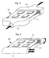
- Figures 1 and 2 illustrate an example of a printed circuit board SMI comprising a substrate constituting a first embodiment of the present invention.
- the reference numeral 1 designates the substrate according to the present invention and the reference numeral 2 denotes a electrical circuit arrangement for receiving components surface mounted electronics.
- an electronic component 3 arranged on the surface of the arrangement electrical circuit board 2.
- the substrate 1 comprises on the one hand a base substrate 11 made of a thermally conductive material and on the other hand, means of electrical insulation and thermal conduction, indicated by the reference numeral 12, making it possible to ensure the transfer towards the base substrate 11 of the heat dissipated by the components electronic.
- these means 12 comprise, arranged on one face of the base substrate 11, a layer having both electrical insulating properties and thermally conductive.
- means of isolation electrical and thermal conduction can advantageously be arranged on either side of the base substrate 11 so as to allow the provision of an electrical arrangement in printed circuit on each of the faces of the substrate of the present invention.
- the electrical arrangement in printed circuit 2 includes a deposit metallic conductive 21 deposited on the surface of the insulation means electric and thermal conduction 12, and forming connection tracks electrical 22 for electronic components.
- the electronic component 3 disposed on the surface of the electrical arrangement in printed circuit 2 thus comprises connection lugs 31 respectively connected to the electrical connection tracks 22.
- the conductive metallic deposit 21 is preferably made of copper and can for example be formed from a sheet made integral with the substrate or be obtained by electrodeposition. Conventional training processes of printed circuits, well known to those skilled in the art, allow by elsewhere to form the electrical connection tracks 22 from this deposit metallic.
- the base substrate 11 can be made of a good material thermally conductive such as a selected metallic material in the group of materials comprising in particular aluminum AI, copper Cu, steel, and alloys or combinations of these materials. Note that this list is not exhaustive because other equivalent materials having good thermal conductivity can be used.
- the substrate of base 11 is preferably made of aluminum because it combines material advantageously a low weight and excellent thermal conductivity.
- the layer forming the means of electrical insulation and thermal conduction 12 for example it is necessary to use an epoxy resin or a polyimide film (amide) charged with particles promoting good thermal conductivity such as ceramic particles or glass fibers for example.
- an epoxy resin or a polyimide film (amide) charged with particles promoting good thermal conductivity such as ceramic particles or glass fibers for example.
- the means of electrical insulation and heat conduction 12 may include a plurality of layers superimposed having in combination insulating properties from the point of view electric and thermally conductive.
- combinations of epoxy films and polyimide (amide) films can be considered.
- adhesives used to secure the different layers of the substrate and the printed circuit can also enter into the composition of these means of electrical insulation and thermal conduction.
- the base substrate 11 includes heat removal means formed in this example of a plurality of channels 15 formed in the plane of the base substrate 11 and which are understood in a direction D or direction of flow indicated by an arrow in the figures.
- These channels 15 are intended to allow the circulation of a cooling, such as a gaseous compound or preferably a liquid, of so as to ensure a heat exchange between this coolant and the base substrate 11 and thus more efficiently dissipate the heat transmitted in the base substrate 11 by the electronic components mounted in area .
- a cooling such as a gaseous compound or preferably a liquid
- the base substrate 11 is subjected directly to the cooling action of the coolant.
- the capacity of thermal evacuation of the substrate according to the present invention is thus increased.
- the channels 15 are formed in the thickness of the base substrate 11 and therefore have a closed section.
- the section of these channels can have very diverse shapes (elliptical sections, oblong, rectangular, polygonal, etc.). More specifically, the shape of these channels is determined, on the one hand, by the thermal requirements, to know the amount of heat to be removed from the substrate, and, on the other hand, by the process for manufacturing or machining the substrate.
- the base substrate 11 can for example very advantageously be produced by a conventional extrusion process of a profile made of material metallic. This manufacturing process makes it possible in particular to produce metal plates of great length and constant section at relatively low costs. As such, it should be noted that aluminum lends itself particularly good at this type of manufacturing process.
- the substrate according to the present invention thus has the advantage to be of smaller dimensions compared to the structures of the prior art which require the addition of an additional radiator element.
- the substrate according to the present invention has a heat removal efficiency of up to a factor of 1 to 2 orders of magnitude higher than the efficiency of an SMI substrate conventional when the coolant used is a liquid.
- the application of an unforced gas or a pulsed gas already allows to increase significantly the effectiveness of the substrate.
- the channels 15 therefore preferably have a cross-section of small area and are produced in large numbers. It should also be noted that the realization of small diameter channels promotes flow turbulent coolant regime.
- the production by extrusion of a metal profile is particularly suitable for producing a base substrate having the characteristics mentioned above. Note, however, that it is possible to use other manufacturing techniques to make a base substrate comprising cooling channels. For example, it would possible to use a sintering process, that is to say molding of metallic powders to obtain a base substrate having similar characteristics.
- the channels 15 are preferably formed in the base substrate 11 so as to be distant from the face on which the means rest of electrical insulation and thermal conduction 12 by a determined distance e as illustrated in figure 2.
- This distance e between the channels 15 and the means 12 defines an area in a first thickness of the base substrate 11 for temporarily accumulating heat dissipated by electronic components. This area of the base substrate is thus intended to play the role of a thermal mass.
- this thermal mass are determined mainly according to the power dissipated by the components electronic devices mounted on the surface as well as on the surface of the printed circuit. It must allow the heat dissipated on the surface to be "drained” quickly by electronic components, especially when these generate short warm-ups. Indeed, if this thermal mass is insufficiently dimensioned, the heat dissipated momentarily by the electronic components can remain localized on the surface and cause damage to the printed circuit and electronic components.
- the mass thermal thus ensures that the heat dissipated by the components surface mounted electronics be removed from the surface as quickly as possible of the printed circuit to be first accumulated in the substrate of base 11, then be evacuated under the action of the circulating coolant through channels 15.
- this thermal mass should be dimensioned with a thickness e of l '' from 2 to 5 mm.
- FIG. 3 a device will be described making it possible to integrate in a cooling circuit an electronic module, indicated by the reference numeral 50, formed on an insulated metal substrate according to the present invention.
- an input connector 61 is connected to a end of the electronic module 50, and an output connector 62 is connected to the other end of module 50, so that the circulation coolant in the direction of flow indicated by the arrow is ensured through the channels (not shown in this figure) formed in the base substrate, indicated by the reference numeral 11, of the module 50.
- FIG. 4 illustrates another example of a base substrate that can be considered in the context of the present invention.
- This figure thus illustrates a base substrate 11A comprising a plurality of channels 15A located in an upper part of the base substrate 11A and at least one channel 15B located in a lower part of the base substrate 11A.
- channels 15A are intended to ensure the circulation of the coolant in a first direction flow
- the channel 15B is intended to ensure the circulation of this fluid in a direction opposite to this direction of flow.
- Channels 15A and 15B thus form respectively a outward journey and a return journey for the coolant passing through the base substrate 11A.
- FIG. 5 illustrates a device making it possible to integrate into a circuit of cooling an electronic module, indicated by the reference numeral 50A, formed on a metal substrate comprising a base substrate of the type illustrated in Figure 4 and indicated by the same reference numeral 11A.
- an input-output connector 71 is connected to one end of the module 50A, and a return connector 72 is disposed at the other end of the module 50A.
- the input-output connector 71 is arranged so as to connect, at the input, the channels located in the upper part of the base substrate 11A of the module 50A (namely the channels 15A in FIG. 4) and, at the outlet, the channel or channels located in the lower part of the base substrate 11A (namely the channel 15B in the figure 4).
- the return connector 72 ensures a connection between the upper and lower channels of the substrate.
- input connectors 61 and output and 62 of figure 3 can be formulated regarding input-output connectors 71 and return connectors 72.
- these connectors can for example be made of material plastic or metallic material.
- a connector input-output and a return connector to integrate into a circuit cooling a module produced on a substrate of the type illustrated in the figures 1 and 2.
- part of the channels will be used to ensure the circulation go of the coolant and the other part of the channels will used to ensure the return circulation of the cooling fluid.
- the input-output and return connectors will naturally be made of so that the channels are properly connected.
- the isolated metal substrate according to the present invention advantageously makes it possible to get rid of the use of an additional radiator element, in particular in high or very high power applications.
- the solution according to this invention thus frees both sides of the base substrate and thus authorizes the arrangement of two electrical arrangements in circuit printed on both sides of the insulated metal substrate which was not possible with the solutions of the prior art, or at least was not possible at such small dimensions.
Priority Applications (1)
| Application Number | Priority Date | Filing Date | Title |
|---|---|---|---|
| EP99108065A EP1047294A1 (de) | 1999-04-23 | 1999-04-23 | Isoliertes metallisches Substrat für Leiterplatten |
Applications Claiming Priority (1)
| Application Number | Priority Date | Filing Date | Title |
|---|---|---|---|
| EP99108065A EP1047294A1 (de) | 1999-04-23 | 1999-04-23 | Isoliertes metallisches Substrat für Leiterplatten |
Publications (1)
| Publication Number | Publication Date |
|---|---|
| EP1047294A1 true EP1047294A1 (de) | 2000-10-25 |
Family
ID=8238031
Family Applications (1)
| Application Number | Title | Priority Date | Filing Date |
|---|---|---|---|
| EP99108065A Withdrawn EP1047294A1 (de) | 1999-04-23 | 1999-04-23 | Isoliertes metallisches Substrat für Leiterplatten |
Country Status (1)
| Country | Link |
|---|---|
| EP (1) | EP1047294A1 (de) |
Cited By (15)
| Publication number | Priority date | Publication date | Assignee | Title |
|---|---|---|---|---|
| WO2002039241A2 (de) * | 2000-11-13 | 2002-05-16 | P21 - Power For The 21St Century Gmbh | Elektrisches bauteil |
| WO2003025476A2 (en) * | 2001-09-07 | 2003-03-27 | Raytheon Company | Microelectronic system with integral cyrocooler, and its fabrication and use |
| DE10203238A1 (de) * | 2002-01-28 | 2003-06-05 | Siemens Ag | Kühlbaustein |
| DE10203239A1 (de) * | 2002-01-28 | 2003-06-05 | Siemens Ag | Kühlbaustein |
| WO2003063567A1 (en) * | 2002-01-16 | 2003-07-31 | Rockwell Automation Technologies, Inc. | Modular power converter having fluid cooled support |
| DE10338469A1 (de) * | 2003-08-21 | 2004-11-25 | Siemens Ag | Stromrichtermodul mit einer rückwärtigen Kühlplatte |
| EP1837909A1 (de) * | 2005-01-14 | 2007-09-26 | Mitsubishi Denki Kabushiki Kaisha | Kühlkörper und kühleinheit damit |
| DE102007053090A1 (de) * | 2007-11-07 | 2009-05-20 | Rohde & Schwarz Gmbh & Co. Kg | Kühlkörper für elektronische Bauelemente und Verfahren zur Herstellung eines Kühlkörpers für elektronische Bauelemente |
| WO2012146335A1 (de) * | 2011-04-28 | 2012-11-01 | Sew-Eurodrive Gmbh & Co. Kg | Anordnung zum temperieren, insbesondere kühlen, von wärmeerzeugenden bauelementen mit einer kühlplatte |
| EP2226550B1 (de) * | 2009-03-04 | 2015-03-04 | Zumtobel Lighting GmbH | LED-Leuchte mit Kühlkanal |
| WO2015160910A1 (en) * | 2014-04-16 | 2015-10-22 | Raytheon Company | Monolithic multi-module electronics chassis with multi-planar embedded fluid cooling channels |
| CN107613653A (zh) * | 2017-09-20 | 2018-01-19 | 四川海英电子科技有限公司 | 高多阶hdi印刷电路板的制作方法 |
| CN107613652A (zh) * | 2017-09-20 | 2018-01-19 | 四川海英电子科技有限公司 | 高密度互联印刷电路板的制造方法 |
| CN107660067A (zh) * | 2017-11-07 | 2018-02-02 | 百硕电脑(苏州)有限公司 | 大功率led线路板 |
| CN112996232A (zh) * | 2021-02-26 | 2021-06-18 | 赣州新联兴科技有限公司 | 一种pcb基材及5g基站用高频高速pcb板 |
Citations (5)
| Publication number | Priority date | Publication date | Assignee | Title |
|---|---|---|---|---|
| US4718163A (en) * | 1981-12-31 | 1988-01-12 | Thomson-Csf | Process for producing cooling device for printed circuit card |
| US4767674A (en) * | 1984-01-27 | 1988-08-30 | Dainichi-Nippon Cables, Ltd. | Metal cored board and method for manufacturing same |
| DE4019743A1 (de) * | 1990-06-21 | 1992-01-02 | Standard Elektrik Lorenz Ag | Kuehlmittelanschlussvorrichtung fuer ein- oder mehrlagige leiterplatten mit einer kuehlvorrichtung |
| JPH0461193A (ja) * | 1990-06-22 | 1992-02-27 | Murata Mfg Co Ltd | 金属ベース配線基板の製造方法 |
| DE29805944U1 (de) * | 1998-03-26 | 1998-06-10 | Abb Daimler Benz Transp | Stranghohlprofil für wassergekühlte, leistungselektronische Komponenten |
-
1999
- 1999-04-23 EP EP99108065A patent/EP1047294A1/de not_active Withdrawn
Patent Citations (5)
| Publication number | Priority date | Publication date | Assignee | Title |
|---|---|---|---|---|
| US4718163A (en) * | 1981-12-31 | 1988-01-12 | Thomson-Csf | Process for producing cooling device for printed circuit card |
| US4767674A (en) * | 1984-01-27 | 1988-08-30 | Dainichi-Nippon Cables, Ltd. | Metal cored board and method for manufacturing same |
| DE4019743A1 (de) * | 1990-06-21 | 1992-01-02 | Standard Elektrik Lorenz Ag | Kuehlmittelanschlussvorrichtung fuer ein- oder mehrlagige leiterplatten mit einer kuehlvorrichtung |
| JPH0461193A (ja) * | 1990-06-22 | 1992-02-27 | Murata Mfg Co Ltd | 金属ベース配線基板の製造方法 |
| DE29805944U1 (de) * | 1998-03-26 | 1998-06-10 | Abb Daimler Benz Transp | Stranghohlprofil für wassergekühlte, leistungselektronische Komponenten |
Non-Patent Citations (1)
| Title |
|---|
| PATENT ABSTRACTS OF JAPAN vol. 016, no. 263 (E - 1216) 15 June 1992 (1992-06-15) * |
Cited By (24)
| Publication number | Priority date | Publication date | Assignee | Title |
|---|---|---|---|---|
| WO2002039241A2 (de) * | 2000-11-13 | 2002-05-16 | P21 - Power For The 21St Century Gmbh | Elektrisches bauteil |
| WO2002039241A3 (de) * | 2000-11-13 | 2003-02-27 | P21 Gmbh | Elektrisches bauteil |
| WO2003025476A2 (en) * | 2001-09-07 | 2003-03-27 | Raytheon Company | Microelectronic system with integral cyrocooler, and its fabrication and use |
| WO2003025476A3 (en) * | 2001-09-07 | 2004-02-05 | Raytheon Co | Microelectronic system with integral cyrocooler, and its fabrication and use |
| WO2003063567A1 (en) * | 2002-01-16 | 2003-07-31 | Rockwell Automation Technologies, Inc. | Modular power converter having fluid cooled support |
| US6940715B2 (en) | 2002-01-16 | 2005-09-06 | Rockwell Automation Technologies, Inc. | Modular power converter having fluid cooled support |
| DE10203238A1 (de) * | 2002-01-28 | 2003-06-05 | Siemens Ag | Kühlbaustein |
| DE10203239A1 (de) * | 2002-01-28 | 2003-06-05 | Siemens Ag | Kühlbaustein |
| DE10338469A1 (de) * | 2003-08-21 | 2004-11-25 | Siemens Ag | Stromrichtermodul mit einer rückwärtigen Kühlplatte |
| EP1837909A1 (de) * | 2005-01-14 | 2007-09-26 | Mitsubishi Denki Kabushiki Kaisha | Kühlkörper und kühleinheit damit |
| US8225854B2 (en) | 2005-01-14 | 2012-07-24 | Mitsubishi Denki Kabushiki Kaisha | Heat sink and cooling unit using the same |
| EP1837909A4 (de) * | 2005-01-14 | 2011-03-02 | Mitsubishi Electric Corp | Kühlkörper und kühleinheit damit |
| DE102007053090B4 (de) * | 2007-11-07 | 2011-12-15 | Rohde & Schwarz Gmbh & Co. Kg | Kühlkörper und Kühlanordnung für elektrische Komponenten und Verfahren zur Herstellung eines Kühlkörpers und einer Kühlanordnung für elektrische Komponenten |
| DE102007053090A1 (de) * | 2007-11-07 | 2009-05-20 | Rohde & Schwarz Gmbh & Co. Kg | Kühlkörper für elektronische Bauelemente und Verfahren zur Herstellung eines Kühlkörpers für elektronische Bauelemente |
| EP2226550B1 (de) * | 2009-03-04 | 2015-03-04 | Zumtobel Lighting GmbH | LED-Leuchte mit Kühlkanal |
| WO2012146335A1 (de) * | 2011-04-28 | 2012-11-01 | Sew-Eurodrive Gmbh & Co. Kg | Anordnung zum temperieren, insbesondere kühlen, von wärmeerzeugenden bauelementen mit einer kühlplatte |
| EP2702845B1 (de) * | 2011-04-28 | 2017-08-16 | Sew-Eurodrive GmbH & Co. KG | Anordnung zum temperieren, insbesondere kühlen, von wärmeerzeugenden bauelementen mit einer kühlplatte |
| WO2015160910A1 (en) * | 2014-04-16 | 2015-10-22 | Raytheon Company | Monolithic multi-module electronics chassis with multi-planar embedded fluid cooling channels |
| US9468131B2 (en) | 2014-04-16 | 2016-10-11 | Raytheon Company | Monolithic multi-module electronics chassis with multi-planar embedded fluid cooling channels |
| CN107613653A (zh) * | 2017-09-20 | 2018-01-19 | 四川海英电子科技有限公司 | 高多阶hdi印刷电路板的制作方法 |
| CN107613652A (zh) * | 2017-09-20 | 2018-01-19 | 四川海英电子科技有限公司 | 高密度互联印刷电路板的制造方法 |
| CN107660067A (zh) * | 2017-11-07 | 2018-02-02 | 百硕电脑(苏州)有限公司 | 大功率led线路板 |
| CN112996232A (zh) * | 2021-02-26 | 2021-06-18 | 赣州新联兴科技有限公司 | 一种pcb基材及5g基站用高频高速pcb板 |
| CN112996232B (zh) * | 2021-02-26 | 2022-02-18 | 赣州新联兴科技有限公司 | 一种5g基站用高频高速pcb板 |
Similar Documents
| Publication | Publication Date | Title |
|---|---|---|
| EP1243169B1 (de) | Elektronische baugruppe mit hohem kühlungsvermögen | |
| EP1047294A1 (de) | Isoliertes metallisches Substrat für Leiterplatten | |
| EP1792526B1 (de) | Mit integriertem wärmeverteiler ausgestattete elektronische einrichtung | |
| FR2741196A1 (fr) | Module de conversion thermoelectrique et procede de fabrication d'un tel module | |
| FR2829874A1 (fr) | Systeme a semi-conducteur a boitier et enveloppe | |
| EP0197817A1 (de) | Gedruckte Schaltplatte mit Wärmeumtauscher und Verfahren zu deren Herstellung | |
| FR2744873A1 (fr) | Corps de refroidissement pour composants electriques ou electroniques | |
| FR3018989A1 (fr) | Module electronique, notamment pour un appareil de commande de boite de vitesses | |
| EP1550361B1 (de) | Dreidimensionales elektronisches modul | |
| EP1116424B1 (de) | Elektronische baugruppe mit einer wärmeplatte | |
| EP1239515B1 (de) | Substrat für elektronische Leistungsschaltung und elektronisches Leistungsmodul mit diesem | |
| FR2793990A1 (fr) | Boitier electronique sur plaque et procede de fabrication d'un tel boitier | |
| EP0779775B1 (de) | Elektronische Baugruppe mit Wärmeabführung, besonders für Hochspannungsumwandler einer Entladungslampe von Scheinwerfer | |
| EP3966850B1 (de) | Verfahren zur herstellung eines elektronischen leistungsmoduls | |
| FR2706730A1 (fr) | Module électronique de puissance ayant un support d'évacuation de la chaleur. | |
| WO2003096414A2 (fr) | Assemblage de composants de puissance sur un circuit imprime ainsi qu'un procede d'un tel assemblage | |
| WO2002078088A1 (fr) | Assemblage de composants d'epaisseurs diverses | |
| WO2020021197A1 (fr) | Procede de fabrication d'un module electronique de puissance | |
| EP3966851B1 (de) | Verfahren zur herstellung eines elektronischen leistungsmoduls | |
| FR2523397A1 (fr) | Procede de montage de composants electroniques sur un support et produit realisable par le procede | |
| EP3731612B1 (de) | Bedienvorrichtung mit verbesserter kühlung für elektrisches stellglied | |
| EP0090727A1 (de) | Elektrische und thermische gedruckte Leiterplatte, Verfahren zur Herstellung einer solchen Platte, sowie elektrisches und thermisches Steckverbindungssystem unter Verwendung einer solchen Platte | |
| FR2699039A1 (fr) | Carte électronique à substrat multicouche. | |
| WO2022128457A1 (fr) | Module thermoélectrique et échangeur thermique associé | |
| EP2500937B1 (de) | Elektronischer Schaltkreis mit Doppelisolierschicht, und sein Herstellungsverfahren |
Legal Events
| Date | Code | Title | Description |
|---|---|---|---|
| PUAI | Public reference made under article 153(3) epc to a published international application that has entered the european phase |
Free format text: ORIGINAL CODE: 0009012 |
|
| AK | Designated contracting states |
Kind code of ref document: A1 Designated state(s): AT BE CH CY DE DK ES FI FR GB GR IE IT LI LU MC NL PT SE |
|
| AX | Request for extension of the european patent |
Free format text: AL;LT;LV;MK;RO;SI |
|
| AKX | Designation fees paid | ||
| STAA | Information on the status of an ep patent application or granted ep patent |
Free format text: STATUS: THE APPLICATION IS DEEMED TO BE WITHDRAWN |
|
| 18D | Application deemed to be withdrawn |
Effective date: 20010426 |
|
| REG | Reference to a national code |
Ref country code: DE Ref legal event code: 8566 |