EP1047290A2 - Printing wiring board - Google Patents
Printing wiring board Download PDFInfo
- Publication number
- EP1047290A2 EP1047290A2 EP00303444A EP00303444A EP1047290A2 EP 1047290 A2 EP1047290 A2 EP 1047290A2 EP 00303444 A EP00303444 A EP 00303444A EP 00303444 A EP00303444 A EP 00303444A EP 1047290 A2 EP1047290 A2 EP 1047290A2
- Authority
- EP
- European Patent Office
- Prior art keywords
- wiring board
- printed wiring
- communication lines
- layer
- common mode
- Prior art date
- Legal status (The legal status is an assumption and is not a legal conclusion. Google has not performed a legal analysis and makes no representation as to the accuracy of the status listed.)
- Withdrawn
Links
- 238000004891 communication Methods 0.000 claims abstract description 40
- 239000003990 capacitor Substances 0.000 claims abstract description 16
- 230000004907 flux Effects 0.000 abstract description 38
- 239000007787 solid Substances 0.000 description 16
- 230000000694 effects Effects 0.000 description 6
- 238000010586 diagram Methods 0.000 description 5
- 230000002238 attenuated effect Effects 0.000 description 4
- 230000005855 radiation Effects 0.000 description 3
- 238000000034 method Methods 0.000 description 2
- 230000007613 environmental effect Effects 0.000 description 1
- 239000012212 insulator Substances 0.000 description 1
- 230000010354 integration Effects 0.000 description 1
- 238000010030 laminating Methods 0.000 description 1
- 238000012986 modification Methods 0.000 description 1
- 230000004048 modification Effects 0.000 description 1
- 230000002265 prevention Effects 0.000 description 1
- 230000002285 radioactive effect Effects 0.000 description 1
Images



Classifications
-
- H—ELECTRICITY
- H05—ELECTRIC TECHNIQUES NOT OTHERWISE PROVIDED FOR
- H05K—PRINTED CIRCUITS; CASINGS OR CONSTRUCTIONAL DETAILS OF ELECTRIC APPARATUS; MANUFACTURE OF ASSEMBLAGES OF ELECTRICAL COMPONENTS
- H05K1/00—Printed circuits
- H05K1/02—Details
- H05K1/0213—Electrical arrangements not otherwise provided for
- H05K1/0216—Reduction of cross-talk, noise or electromagnetic interference
- H05K1/023—Reduction of cross-talk, noise or electromagnetic interference using auxiliary mounted passive components or auxiliary substances
- H05K1/0231—Capacitors or dielectric substances
-
- H—ELECTRICITY
- H05—ELECTRIC TECHNIQUES NOT OTHERWISE PROVIDED FOR
- H05K—PRINTED CIRCUITS; CASINGS OR CONSTRUCTIONAL DETAILS OF ELECTRIC APPARATUS; MANUFACTURE OF ASSEMBLAGES OF ELECTRICAL COMPONENTS
- H05K2201/00—Indexing scheme relating to printed circuits covered by H05K1/00
- H05K2201/09—Shape and layout
- H05K2201/09209—Shape and layout details of conductors
- H05K2201/0929—Conductive planes
- H05K2201/093—Layout of power planes, ground planes or power supply conductors, e.g. having special clearance holes therein
-
- H—ELECTRICITY
- H05—ELECTRIC TECHNIQUES NOT OTHERWISE PROVIDED FOR
- H05K—PRINTED CIRCUITS; CASINGS OR CONSTRUCTIONAL DETAILS OF ELECTRIC APPARATUS; MANUFACTURE OF ASSEMBLAGES OF ELECTRICAL COMPONENTS
- H05K2201/00—Indexing scheme relating to printed circuits covered by H05K1/00
- H05K2201/09—Shape and layout
- H05K2201/09209—Shape and layout details of conductors
- H05K2201/09654—Shape and layout details of conductors covering at least two types of conductors provided for in H05K2201/09218 - H05K2201/095
- H05K2201/0969—Apertured conductors
-
- H—ELECTRICITY
- H05—ELECTRIC TECHNIQUES NOT OTHERWISE PROVIDED FOR
- H05K—PRINTED CIRCUITS; CASINGS OR CONSTRUCTIONAL DETAILS OF ELECTRIC APPARATUS; MANUFACTURE OF ASSEMBLAGES OF ELECTRICAL COMPONENTS
- H05K2201/00—Indexing scheme relating to printed circuits covered by H05K1/00
- H05K2201/10—Details of components or other objects attached to or integrated in a printed circuit board
- H05K2201/10613—Details of electrical connections of non-printed components, e.g. special leads
- H05K2201/10621—Components characterised by their electrical contacts
- H05K2201/10689—Leaded Integrated Circuit [IC] package, e.g. dual-in-line [DIL]
Definitions
- This invention relates to a printed wiring board.
- a particular printed wiring board to be described below by way of example in illustration of the present invention has a structure which facilitates the improvement of its electromagnetic environmental compatibility (hereinafter abbreviated to EMC).
- Such high-speed digital circuits carry digital signals containing many high-frequenc components. Consequently, it is necessary to suppress radioactive noise due to unnecessary radiation from a printed wiring board having a digital circuit.
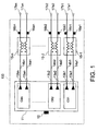
- reference numeral 11 denotes an LSI.
- the LSI 11 has circuit blocks CB1-CBn which are connected to pins 13a1, 13b1 to 13an, 13bn for communication lines and a common E (earth or ground) pin 12.
- the pins 13a1,13b1 to 13an, 13bn for the communication lines are connected to common mode chokes 15-1 to 15-n the prevention of common mode noise via the communication lines 14a1, 14b1 to 14an, 14bn.
- Capacitors 16a1, 16b1 to 16an,16bn having high-frequency characteristics are connected to portions of the communication lines between the common mode chokes 15-1 to 15-n and terminals 17a1, 17b1 to 17an, 17bn.
- the other terminals of the capacitors 16a1, 16b1 to 16an, 16bn are connected to a solid E (earth) layer 32 illustrated in Fig. 2.
- a common mode current la passing through the communication line 14a1 flows along a path which passes via the common mode choke 15-1, capacitor 16a1, solid E layer 32 and communication pin 13a1. Thereby, the common mode current la generates magnetic flux ⁇ a.
- a common mode current Ib passing through the communication line 14b1 flows along a path which passes via the common mode choke 15-1, capacitor 16b1, solid E layer 32 and communication pin 13b1.
- the common mode current Ib generates magnetic flux ⁇ b.
- a printed circuit wiring board will be described below by way of example in illustration of the present invention which is capable of suppressing common mode noise without the use of expensive components, such as a common mode choke as an EMC improving device.
- a printed circuit wiring board has a laminate formed of a pattern-wired layer on which plural communication lines are print-wired, an insulating layer, and a ground layer, the printed wiring board including slotted portions (groove portions) in the sections of the ground layer which are positioned under two parallel-print-wired communication lines, and capacitors between the slotted portions and external connecting terminals of the printed wiring board, the capacitors being connected at one terminal thereof to the communication lines, and at the other terminal thereof to the ground layer via a through hole provided in the insulating layer.
- the width of each of the slotted portions of the first-described printed wiring board is determined on the basis of the distance between the two parallel-print-wired communication lines.
- each of the capacitors in the first-described printed wiring board may be formed by the pattern-wired layer, an insulator being provided on the insulating layer and having a dielectric constant different from that of the insulating layer, and the ground layer.
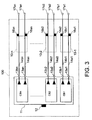
- Fig. 3 illustrates a plan view of a printed circuit wiring board
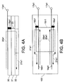
- Fig. 4 illustrates common mode currents flowing in the circuit of the printed circuit wiring board of Fig. 1,
- Fig. 5 is a schematic diagram illustrating the intensity of an electromagnetic wave occurring due to the loop currents shown in Figs. 4,
- Fig. 6 is a schematic diagram illustrating the magnetic flux occurring due to the loop currents shown in Fig. 4,
- Fig. 7 is a plan view of the printed wiring board of Fig. 3 showing two pairs of signal lines print wired adjacently to each other and the common mode currents, and
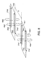
- Fig. 8 is a schematic diagram illustrating the magnetic flux occurring due to the common mode currents of Fig. 7.
- the printed circuit wiring board has elements which are common to those of the previously proposed printed circuit wiring board illustrated in Fig. 1 and which are designated by the same reference numerals, and therefore no further description of them will be made.
- reference numerals 10-1 to 10-n denote slotted portions (or groove portions) provided in a solid E layer 32.
- the slotted portions 10-1 to 10-n are provided so that they are positioned under paired print-wired communication lines 14a1, 14b1 to 14an, and 14bn.
- Fig. 4 illustrates common mode currents 20a1, 20b1 flowing along the communication lines 14a1, 14b1, and common mode currents 21a1, 21b1 flowing through the solid E layer 32. The same applies to the other pairs of communication lines; they are therefore not described here.
- a printed circuit wiring board 100 is formed by laminating a pattern-wired layer 30, on which a wire pattern and parts are provided, an insulating layer 31, and a solid E layer 32.
- the communication line 14a1 is print-wired onto the pattern-wired layer 30. Further, a capacitor 16a1 is connected to the communication line 14a1, and is coupled to the solid E layer 32 via a through hole 33 of the insulating layer 31 at the other terminal thereof. In this case, the communication line 14b1 and a capacitor 16b1 are also connected in the same manner.
- Fig. 5 is a schematic diagram illustrating the intensity of the electromagnetic wave occurring when the common mode currents 20a1, 20b1 flow.
- the intensity E of the electromagnetic wave in a position spaced by a distance (d) from the centre of a loop area S and formed by a frequency (f) and a current I is defined as follows.
- E Kx (Sxlxf 2 /d) sin ⁇
- S represents the area (m 2 ) of a current loop
- I the loop current value (A)
- f the frequency (Hz) of the current loop
- d the distance (m) from the centre of the current loop
- ⁇ the radiation angle (rad) with respect to the Z-axis of the electromagnetic wave
- K a constant.
- the area S, the current I and the frequency (f) must be reduced, and the distance (d) must be increased in order to reduce the intensity of unnecessary radiation due to one loop current.
- Fig. 6 is a schematic diagram illustrating the magnetic flux occurring due to loop currents formed by the common mode currents 20a1, 20b1 flowing in the communication lines 14a1, 14b1 and the common mode currents 21a1, 21b1 flowing through the solid E layer 32.
- the loop current formed by the common mode currents 20a1, 21a1 generate a magnetic flux 40a1 in the slotted portion 10-1.
- the current 21a1 flowing through the solid E layer 32 generates a magnetic flux 41a1. However, this magnetic flux passes through the solid E layer 32.
- this magnetic flux is shielded by the solid E layer 32 and attenuated or caused to decay. Thereby, the intensity thereof is lowered. Consequently, the magnetic flux generated by the loop currents 20a1, 21a1 is constituted mainly by the magnetic flux 40a1 occurring in the slotted portion 10-1.
- the magnetic fluxes 40b1, 41 b1 are generated in the same manner as mentioned above, due to a loop current formed by the common mode currents 20b1, 21 b1. However, the magnetic flux 41 b1 is attenuated due to the shielding effect of the solid E layer 32.
- the magnetic flux occurring due to this loop current is mainly constituted by the magnetic flux 40b1 generated in the slotted portions 10-1.
- the directions of the magnetic fluxes 40a1, 40b1 passing through the slotted portion 10-1 are opposite to each other, and the levels of the same magnetic flux are equal. Therefore, the magnetic fluxes 40a1, 40b1 offset or cancel each other, and have the same effect as that obtained when the magnetic flux ⁇ a, and ⁇ b occurring due to the common mode choke 15-1 offset or cancel each other. This causes the common mode noise level to become lower.
- Fig. 5 illustrates paired adjacently arranged communication lines 14a1, 14b1 and 14a2, 14b2, and Fig. 6 illustrates the magnetic flux occurring due to a loop current flowing in each communication line.
- the slotted portions 10-1 and 10-2 are spaced from each other by a distance D.
- the magnetic flux 40b1 is generated by the common mode current 20b1 on the side of the slotted portion (or groove portion) 10-1 which is adjacent to the slotted portion 10-2.
- the magnetic flux 41 b1 occurring due to the common mode current 21 b1 is attenuated by the shielding effect of the solid E layer 32 as mentioned above. Consequently, only the magnetic flux 40b1 remains.
- magnetic flux 40a2 is generated by a current 20a2, and magnetic flux 41a2 (not shown) is generated by a current 21a2.
- the distance D may be increased by such an amount that it does not cause the magnetic fluxes 41 b1, 41a2 to influence one another other due to the shielding effect of the solid E layer. Thereby, the units of magnetic flux 40a1, 40b1 and 40a2, 40b2 offset or cancel each other, and any common mode noise can be minimised.
Landscapes
- Physics & Mathematics (AREA)
- Electromagnetism (AREA)
- Engineering & Computer Science (AREA)
- Microelectronics & Electronic Packaging (AREA)
- Structure Of Printed Boards (AREA)
- Shielding Devices Or Components To Electric Or Magnetic Fields (AREA)
- Parts Printed On Printed Circuit Boards (AREA)
- Production Of Multi-Layered Print Wiring Board (AREA)
Abstract
Description
Claims (8)
- A printed wiring board, including a ground layer, an insulating layer the ground layer, a pattern wired layer on the insulating layer, a pair of communication lines on the pattern wired layer, a slotted or grooved portion in the ground layer, which portion is positioned under the communication lines, and capacitors between the slotted or grooved portion and external connecting terminals of the printed wiring board.
- A printed wiring board as claimed in claim 1, wherein each of the capacitors is connected to each of the communication lines at one terminal, and is coupled to the ground layer via a through hole at the other terminal.
- A printed wiring board as claimed in claim 2, wherein the through hole is provided in the insulating layer.
- A printed wiring board as claimed in claim 1, wherein the communication lines are connected to a circuit block in an integrated circuit, the integrated circuit being arranged on the printed wiring board.
- A printed wiring board, including, a ground layer, an insulating layer on the ground layer, a pattern wired layer on the insulating layer, plural pairs of communication lines on the pattern wired layer, slotted or grooved portions in the ground layer which portions are positioned under the communication lines, and capacitors between the respective slotted portions and external connecting terminals of the printed wiring board, the widths of the slotted or grooved portions being determined upon the basis of the distance between the respective adjacent pair of communication lines.
- A printed wiring board as claimed in claim 5, wherein each of the capacitors is connected to each of the communication lines at one terminal, and is coupled to the ground layer via a through hole at the other terminal.
- A printed wiring board as claimed in claim 6, wherein the through hole is provided in the insulating layer.
- A printed wiring board as claimed in claim 5, wherein the communication lines are connected to circuit blocks in an integrated circuit, the integrated circuit being arranged on the printed wiring board.
Applications Claiming Priority (2)
| Application Number | Priority Date | Filing Date | Title |
|---|---|---|---|
| JP11420199A JP3456442B2 (en) | 1999-04-21 | 1999-04-21 | Printed wiring board |
| JP11420199 | 1999-04-21 |
Publications (2)
| Publication Number | Publication Date |
|---|---|
| EP1047290A2 true EP1047290A2 (en) | 2000-10-25 |
| EP1047290A3 EP1047290A3 (en) | 2003-05-02 |
Family
ID=14631748
Family Applications (1)
| Application Number | Title | Priority Date | Filing Date |
|---|---|---|---|
| EP00303444A Withdrawn EP1047290A3 (en) | 1999-04-21 | 2000-04-25 | Printing wiring board |
Country Status (6)
| Country | Link |
|---|---|
| US (1) | US6335865B1 (en) |
| EP (1) | EP1047290A3 (en) |
| JP (1) | JP3456442B2 (en) |
| CN (1) | CN1225949C (en) |
| AU (1) | AU761909B2 (en) |
| SG (1) | SG91272A1 (en) |
Families Citing this family (9)
| Publication number | Priority date | Publication date | Assignee | Title |
|---|---|---|---|---|
| JP4562504B2 (en) * | 2004-12-01 | 2010-10-13 | 株式会社リコー | Printed wiring board |
| JP2007309682A (en) * | 2006-05-16 | 2007-11-29 | Renesas Technology Corp | Transmission circuit, connection sheet, probe sheet, probe card, semiconductor inspection apparatus, and semiconductor device manufacturing method |
| KR100834826B1 (en) * | 2007-01-25 | 2008-06-03 | 삼성전자주식회사 | Integrated circuit module structure with reduced handling damage and terminal resistor arrangement method |
| US20100283124A1 (en) * | 2008-02-01 | 2010-11-11 | Renesas Electronics Corporation | Semiconductor device |
| CN102014602B (en) * | 2010-12-17 | 2013-03-06 | 惠州市科信达电子有限公司 | Design method for improving electromagnetic compatibility performance of high-power element and high-power element module |
| CN102080171A (en) * | 2011-02-21 | 2011-06-01 | 美的集团有限公司 | Composite material for manufacturing electric vacuum device |
| CN104378908B (en) * | 2013-08-12 | 2017-06-16 | 鸿富锦精密工业(深圳)有限公司 | Printed circuit board (PCB) |
| JP6563081B1 (en) * | 2018-06-20 | 2019-08-21 | 三菱電機株式会社 | Power converter |
| JP7193510B2 (en) * | 2020-09-28 | 2022-12-20 | 矢崎総業株式会社 | Laminated circuit board device |
Family Cites Families (8)
| Publication number | Priority date | Publication date | Assignee | Title |
|---|---|---|---|---|
| JP2819775B2 (en) * | 1990-05-21 | 1998-11-05 | 日本電気株式会社 | Hybrid integrated circuit device |
| US5068631A (en) * | 1990-08-09 | 1991-11-26 | At&T Bell Laboratories | Sub power plane to provide EMC filtering for VLSI devices |
| JP3265669B2 (en) * | 1993-01-19 | 2002-03-11 | 株式会社デンソー | Printed board |
| DE9412794U1 (en) * | 1994-08-09 | 1995-09-07 | Krone Ag, 14167 Berlin | PCB for connectors |
| JP3513333B2 (en) * | 1995-09-29 | 2004-03-31 | キヤノン株式会社 | Multilayer printed wiring board and electronic equipment mounting the same |
| JP3473319B2 (en) * | 1997-04-30 | 2003-12-02 | 株式会社村田製作所 | Multilayer circuit board |
| JP3476351B2 (en) * | 1997-11-27 | 2003-12-10 | シャープ株式会社 | Low noise amplifier |
| US6488540B2 (en) * | 2000-09-08 | 2002-12-03 | Heyco, Inc. | Multi-receptacle electrical outlet |
-
1999
- 1999-04-21 JP JP11420199A patent/JP3456442B2/en not_active Expired - Fee Related
-
2000
- 2000-04-20 SG SG200002258A patent/SG91272A1/en unknown
- 2000-04-20 US US09/553,478 patent/US6335865B1/en not_active Expired - Fee Related
- 2000-04-20 CN CN00106091.0A patent/CN1225949C/en not_active Expired - Fee Related
- 2000-04-20 AU AU28938/00A patent/AU761909B2/en not_active Ceased
- 2000-04-25 EP EP00303444A patent/EP1047290A3/en not_active Withdrawn
Also Published As
| Publication number | Publication date |
|---|---|
| CN1225949C (en) | 2005-11-02 |
| US6335865B1 (en) | 2002-01-01 |
| SG91272A1 (en) | 2002-09-17 |
| CN1271248A (en) | 2000-10-25 |
| JP2000307205A (en) | 2000-11-02 |
| EP1047290A3 (en) | 2003-05-02 |
| JP3456442B2 (en) | 2003-10-14 |
| AU761909B2 (en) | 2003-06-12 |
| AU2893800A (en) | 2000-10-26 |
Similar Documents
| Publication | Publication Date | Title |
|---|---|---|
| KR920005068B1 (en) | Printed wiring board | |
| JP5409312B2 (en) | Multilayer printed circuit board | |
| EP1047290A2 (en) | Printing wiring board | |
| KR19980087247A (en) | Printed wiring board | |
| EP1255334A1 (en) | Fault tolerant electrical circuit and method | |
| TWM377827U (en) | Ground termination with dampened resonance | |
| KR101656719B1 (en) | Inductor element and integrated circuit device | |
| JP6422395B2 (en) | Circuit board | |
| US6448863B1 (en) | Differential transmission cable and joint with specific distances | |
| JP3666967B2 (en) | Ground connection structure | |
| JP5756910B2 (en) | Printed circuit boards, current sensors and distribution boards | |
| JP5311669B2 (en) | Wiring board | |
| US20100283124A1 (en) | Semiconductor device | |
| JP4371766B2 (en) | Printed wiring board | |
| JPH11177274A (en) | Method of connecting printed wiring board to cable and housing, and electronic device | |
| JP4957543B2 (en) | Printed circuit board | |
| CN109328486A (en) | Shielded three-layer patterned ground structure | |
| JP2008078156A (en) | Modular connector | |
| US20210153342A1 (en) | Printed circuit board structure and method for inductive noise cancellation | |
| JPH0468598A (en) | multilayer wiring circuit board | |
| JP2002171047A (en) | Electronic equipment and flat cable mounting method | |
| JP6399969B2 (en) | Printed board | |
| JP7840587B2 (en) | Current sensor | |
| US12388359B2 (en) | Power conversion device | |
| JP2008078157A (en) | Modular connector |
Legal Events
| Date | Code | Title | Description |
|---|---|---|---|
| PUAI | Public reference made under article 153(3) epc to a published international application that has entered the european phase |
Free format text: ORIGINAL CODE: 0009012 |
|
| AK | Designated contracting states |
Kind code of ref document: A2 Designated state(s): AT BE CH CY DE DK ES FI FR GB GR IE IT LI LU MC NL PT SE |
|
| AX | Request for extension of the european patent |
Free format text: AL;LT;LV;MK;RO;SI |
|
| PUAL | Search report despatched |
Free format text: ORIGINAL CODE: 0009013 |
|
| AK | Designated contracting states |
Designated state(s): AT BE CH CY DE DK ES FI FR GB GR IE IT LI LU MC NL PT SE |
|
| AX | Request for extension of the european patent |
Extension state: AL LT LV MK RO SI |
|
| 17P | Request for examination filed |
Effective date: 20030321 |
|
| AKX | Designation fees paid |
Designated state(s): FR GB IT |
|
| REG | Reference to a national code |
Ref country code: DE Ref legal event code: 8566 |
|
| STAA | Information on the status of an ep patent application or granted ep patent |
Free format text: STATUS: THE APPLICATION HAS BEEN WITHDRAWN |
|
| 18W | Application withdrawn |
Effective date: 20051229 |