EP1047189A2 - Piezoelectric resonator - Google Patents
Piezoelectric resonator Download PDFInfo
- Publication number
- EP1047189A2 EP1047189A2 EP00108101A EP00108101A EP1047189A2 EP 1047189 A2 EP1047189 A2 EP 1047189A2 EP 00108101 A EP00108101 A EP 00108101A EP 00108101 A EP00108101 A EP 00108101A EP 1047189 A2 EP1047189 A2 EP 1047189A2
- Authority
- EP
- European Patent Office
- Prior art keywords
- piezoelectric thin
- piezoelectric
- thin
- film layers
- film
- Prior art date
- Legal status (The legal status is an assumption and is not a legal conclusion. Google has not performed a legal analysis and makes no representation as to the accuracy of the status listed.)
- Granted
Links
- 239000010409 thin film Substances 0.000 claims abstract description 181
- 238000000034 method Methods 0.000 claims description 18
- 239000000463 material Substances 0.000 claims description 9
- XLOMVQKBTHCTTD-UHFFFAOYSA-N Zinc monoxide Chemical compound [Zn]=O XLOMVQKBTHCTTD-UHFFFAOYSA-N 0.000 description 18
- 238000010276 construction Methods 0.000 description 14
- VYPSYNLAJGMNEJ-UHFFFAOYSA-N Silicium dioxide Chemical compound O=[Si]=O VYPSYNLAJGMNEJ-UHFFFAOYSA-N 0.000 description 8
- 239000011787 zinc oxide Substances 0.000 description 8
- 230000005284 excitation Effects 0.000 description 7
- 229910052814 silicon oxide Inorganic materials 0.000 description 7
- 239000000758 substrate Substances 0.000 description 7
- 230000005684 electric field Effects 0.000 description 6
- 230000000644 propagated effect Effects 0.000 description 6
- 230000008878 coupling Effects 0.000 description 4
- 238000010168 coupling process Methods 0.000 description 4
- 238000005859 coupling reaction Methods 0.000 description 4
- 230000010287 polarization Effects 0.000 description 4
- XUIMIQQOPSSXEZ-UHFFFAOYSA-N Silicon Chemical compound [Si] XUIMIQQOPSSXEZ-UHFFFAOYSA-N 0.000 description 3
- 239000010408 film Substances 0.000 description 3
- 229910052710 silicon Inorganic materials 0.000 description 3
- 239000010703 silicon Substances 0.000 description 3
- 230000000052 comparative effect Effects 0.000 description 2
- 238000006073 displacement reaction Methods 0.000 description 2
- HFGPZNIAWCZYJU-UHFFFAOYSA-N lead zirconate titanate Chemical compound [O-2].[O-2].[O-2].[O-2].[O-2].[Ti+4].[Zr+4].[Pb+2] HFGPZNIAWCZYJU-UHFFFAOYSA-N 0.000 description 2
- 238000004088 simulation Methods 0.000 description 2
- VYZAMTAEIAYCRO-UHFFFAOYSA-N Chromium Chemical compound [Cr] VYZAMTAEIAYCRO-UHFFFAOYSA-N 0.000 description 1
- RYGMFSIKBFXOCR-UHFFFAOYSA-N Copper Chemical compound [Cu] RYGMFSIKBFXOCR-UHFFFAOYSA-N 0.000 description 1
- 229910003327 LiNbO3 Inorganic materials 0.000 description 1
- XAGFODPZIPBFFR-UHFFFAOYSA-N aluminium Chemical compound [Al] XAGFODPZIPBFFR-UHFFFAOYSA-N 0.000 description 1
- 229910052782 aluminium Inorganic materials 0.000 description 1
- 238000004364 calculation method Methods 0.000 description 1
- 238000005229 chemical vapour deposition Methods 0.000 description 1
- 229910052804 chromium Inorganic materials 0.000 description 1
- 239000011651 chromium Substances 0.000 description 1
- 239000002131 composite material Substances 0.000 description 1
- 229910052802 copper Inorganic materials 0.000 description 1
- 239000010949 copper Substances 0.000 description 1
- 238000013016 damping Methods 0.000 description 1
- 230000007423 decrease Effects 0.000 description 1
- 230000000593 degrading effect Effects 0.000 description 1
- 238000005530 etching Methods 0.000 description 1
- PCHJSUWPFVWCPO-UHFFFAOYSA-N gold Chemical compound [Au] PCHJSUWPFVWCPO-UHFFFAOYSA-N 0.000 description 1
- 229910052737 gold Inorganic materials 0.000 description 1
- 239000010931 gold Substances 0.000 description 1
- 238000010030 laminating Methods 0.000 description 1
- 238000001259 photo etching Methods 0.000 description 1
- 239000010453 quartz Substances 0.000 description 1
- 239000007787 solid Substances 0.000 description 1
- 238000004544 sputter deposition Methods 0.000 description 1
- 230000000087 stabilizing effect Effects 0.000 description 1
- 238000007736 thin film deposition technique Methods 0.000 description 1
- 238000007738 vacuum evaporation Methods 0.000 description 1
Images


Classifications
-
- H—ELECTRICITY
- H03—ELECTRONIC CIRCUITRY
- H03H—IMPEDANCE NETWORKS, e.g. RESONANT CIRCUITS; RESONATORS
- H03H9/00—Networks comprising electromechanical or electro-acoustic elements; Electromechanical resonators
- H03H9/02—Details
- H03H9/02007—Details of bulk acoustic wave devices
- H03H9/02015—Characteristics of piezoelectric layers, e.g. cutting angles
-
- H—ELECTRICITY
- H03—ELECTRONIC CIRCUITRY
- H03H—IMPEDANCE NETWORKS, e.g. RESONANT CIRCUITS; RESONATORS
- H03H3/00—Apparatus or processes specially adapted for the manufacture of impedance networks, resonating circuits, resonators
- H03H3/007—Apparatus or processes specially adapted for the manufacture of impedance networks, resonating circuits, resonators for the manufacture of electromechanical resonators or networks
- H03H3/02—Apparatus or processes specially adapted for the manufacture of impedance networks, resonating circuits, resonators for the manufacture of electromechanical resonators or networks for the manufacture of piezoelectric or electrostrictive resonators or networks
-
- H—ELECTRICITY
- H03—ELECTRONIC CIRCUITRY
- H03H—IMPEDANCE NETWORKS, e.g. RESONANT CIRCUITS; RESONATORS
- H03H9/00—Networks comprising electromechanical or electro-acoustic elements; Electromechanical resonators
- H03H9/15—Constructional features of resonators consisting of piezoelectric or electrostrictive material
- H03H9/17—Constructional features of resonators consisting of piezoelectric or electrostrictive material having a single resonator
- H03H9/178—Constructional features of resonators consisting of piezoelectric or electrostrictive material having a single resonator of a laminated structure of multiple piezoelectric layers with inner electrodes
-
- H—ELECTRICITY
- H03—ELECTRONIC CIRCUITRY
- H03H—IMPEDANCE NETWORKS, e.g. RESONANT CIRCUITS; RESONATORS
- H03H9/00—Networks comprising electromechanical or electro-acoustic elements; Electromechanical resonators
- H03H9/02—Details
- H03H9/02007—Details of bulk acoustic wave devices
- H03H9/02062—Details relating to the vibration mode
- H03H9/02078—Details relating to the vibration mode the vibration mode being overmoded
-
- H—ELECTRICITY
- H03—ELECTRONIC CIRCUITRY
- H03H—IMPEDANCE NETWORKS, e.g. RESONANT CIRCUITS; RESONATORS
- H03H9/00—Networks comprising electromechanical or electro-acoustic elements; Electromechanical resonators
- H03H9/02—Details
- H03H9/02007—Details of bulk acoustic wave devices
- H03H9/02086—Means for compensation or elimination of undesirable effects
-
- H—ELECTRICITY
- H03—ELECTRONIC CIRCUITRY
- H03H—IMPEDANCE NETWORKS, e.g. RESONANT CIRCUITS; RESONATORS
- H03H9/00—Networks comprising electromechanical or electro-acoustic elements; Electromechanical resonators
- H03H9/15—Constructional features of resonators consisting of piezoelectric or electrostrictive material
- H03H9/17—Constructional features of resonators consisting of piezoelectric or electrostrictive material having a single resonator
- H03H9/171—Constructional features of resonators consisting of piezoelectric or electrostrictive material having a single resonator implemented with thin-film techniques, i.e. of the film bulk acoustic resonator [FBAR] type
-
- H—ELECTRICITY
- H03—ELECTRONIC CIRCUITRY
- H03H—IMPEDANCE NETWORKS, e.g. RESONANT CIRCUITS; RESONATORS
- H03H9/00—Networks comprising electromechanical or electro-acoustic elements; Electromechanical resonators
- H03H9/02—Details
- H03H9/02007—Details of bulk acoustic wave devices
- H03H9/02086—Means for compensation or elimination of undesirable effects
- H03H9/02094—Means for compensation or elimination of undesirable effects of adherence
-
- H—ELECTRICITY
- H03—ELECTRONIC CIRCUITRY
- H03H—IMPEDANCE NETWORKS, e.g. RESONANT CIRCUITS; RESONATORS
- H03H9/00—Networks comprising electromechanical or electro-acoustic elements; Electromechanical resonators
- H03H9/15—Constructional features of resonators consisting of piezoelectric or electrostrictive material
- H03H9/17—Constructional features of resonators consisting of piezoelectric or electrostrictive material having a single resonator
- H03H9/171—Constructional features of resonators consisting of piezoelectric or electrostrictive material having a single resonator implemented with thin-film techniques, i.e. of the film bulk acoustic resonator [FBAR] type
- H03H9/172—Means for mounting on a substrate, i.e. means constituting the material interface confining the waves to a volume
- H03H9/173—Air-gaps
-
- H—ELECTRICITY
- H03—ELECTRONIC CIRCUITRY
- H03H—IMPEDANCE NETWORKS, e.g. RESONANT CIRCUITS; RESONATORS
- H03H9/00—Networks comprising electromechanical or electro-acoustic elements; Electromechanical resonators
- H03H9/15—Constructional features of resonators consisting of piezoelectric or electrostrictive material
- H03H9/17—Constructional features of resonators consisting of piezoelectric or electrostrictive material having a single resonator
- H03H9/171—Constructional features of resonators consisting of piezoelectric or electrostrictive material having a single resonator implemented with thin-film techniques, i.e. of the film bulk acoustic resonator [FBAR] type
- H03H9/172—Means for mounting on a substrate, i.e. means constituting the material interface confining the waves to a volume
- H03H9/174—Membranes
Definitions
- the present invention relates to a multilayer piezoelectric resonator making use of a higher-order vibration mode which is to be used, for example, in an oscillator, filter, etc.
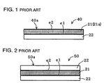
- a conventional piezoelectric resonator 40 using a thickness extensional vibration mode is shown in Fig. 1.
- a vibrator portion 40a is formed by a piezoelectric thin-film layer 21 (having thin-film electrodes e1 and e2 laminated on opposite sides of a piezoelectric thin film 21a) and an insulating thin film layer 22.
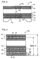
- Another conventional piezoelectric resonator is shown in Fig. 2.
- a vibrator portion 50a is formed by laminating an insulating thin film layer 22, a piezoelectric thin-film layer 21, and an insulating thin film layer 22.
- the term "thin-film” refers to films having a thickness in the range of about 0.01 to 100 ⁇ m.
- the thickness of the vibrator portions 40a and 50a must be reduced because the resonance frequencies are inversely proportional to the thickness of the vibrator portions 40a and 50a.
- the thickness of the vibrator portion 40a when zinc oxide (ZnO) is used for the piezoelectric thin film 21a, the thickness of the vibrator portion 40a must be made as thin as about 4.7 ⁇ m in order to realize a resonance frequency of 650 MHz.
- the mechanical strength of the vibrator portion 40a decreases and the vibrator portion 40a becomes easily damaged.
- the ratio of the thickness of the thin-film electrodes e2 and e2 to the thickness of the vibrator portions 40a and 50a increases, there is also a problem that the damping is increased and the mechanical Q of the resonance is reduced.
- the present invention provides a piezoelectric resonator which can effectively operate in a higher-order vibration mode with a high resonance frequency while maintaining the mechanical strength of the vibrator portion.
- the piezoelectric resonator is used in conjunction with a voltage source, the combination comprising:
- the invention comprises a method for exciting a piezoelectric resonator in a thickness extensional vibration mode, the piezoelectric resonator comprising a vibrator portion made up of n layers of piezoelectric thin-film, n being an integer greater of equal to 2, each of the piezoelectric thin-film layers being separated by a respective insulating thin-film layer, the method comprising:
- the vibrator portion preferably has a thickness t equal to half the first (basic) resonance wavelength of a thickness extensional vibration mode of the resonator.
- the resonator is excited in a nth (second or higher) higher-order vibration mode by applying appropriate alternating voltages to the piezoelectric thin-film layer.
- the alternating voltages are applied in such a manner that the vibrations induced in adjacent piezoelectric thin-film layers are opposite in phase. This can be done, for example, by applying alternating voltages of opposite phase to the adjacent piezoelectric thin-film layers when the polarization direction of those layers is the same.
- alternating voltages of the same phase can be applied to adjacent piezoelectric thin film layers when the polarization direction of those layers is opposite to one another.
- Each of the piezoelectric thin-film layers is preferably formed at a respective nodal point of the nth higher-order vibration mode.
- the first (basic) vibration mode or lower-order vibration modes lower than the nth mode disappear or attenuate by canceling each other due to the interference of opposite phase mechanical vibrations of the piezoelectric thin-film layers, and only the nth higher-order vibration mode is predominantly excited.
- the electromechanical coupling coefficient of the piezoelectric resonator is large and a sharp resonance curve can be obtained.
- the thickness t of vibrator portion is equal to one half of the resonance wavelength of the basic vibration mode, high resonance frequencies of short wavelengths can be obtained for a given thickness of the vibrator portion. This makes it possible to produce vibrations having higher frequencies without degrading the strength of the vibrator portion.
- the piezoelectric thin-films and insulating thin film layers are preferably composed of materials where the temperature coefficient of the elastic constants is of opposite sign. As a result, the temperature coefficient of the elastic constants of the piezoelectric thin-film layers and insulating thin film layers offset one another, thereby stabilizing the frequency-temperature characteristics of the piezoelectric portion.
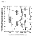
- a piezoelectric resonator 10 of an embodiment of the present invention is described with reference to Fig. 3.
- a silicon supporting substrate 11 has n + 1 layers (n being an integer greater than or equal to 2) of silicon oxide (SiO 2 ) film 12 and n layers of piezoelectric thin-film 1 through n formed thereon.
- Thin-film electrodes e1 and e2 are formed respectively on opposite surfaces of each piezoelectric thin-film layer.
- the piezoelectric resonator 10 of this multilayer construction is preferably formed by appropriately using thin-film deposition techniques such as sputtering, chemical vapor deposition, vacuum evaporation, etc. and photo etching techniques.
- the process is initiated by providing a silicon substrate (a master substrate formed of the supporting material 11).
- An insulating thin film 12 is deposited on the top surface of the substrate 11.
- An electrode thin film such as copper, aluminum, gold/chromium, etc. is then deposited on that layer to form a thin-film electrode e1 of an appropriate shape.
- a piezoelectric thin film composed of piezoelectric materials such as zinc oxide (ZnO), lead titanate zirconate, etc. is deposited on the electrode e1 and the exposed portion of the lower insulating thin film 12.
- An electrode thin film is deposited on the piezoelectric thin film and is appropriately patterned to form a thin-film electrode e2.
- the thin-film electrode e1 (as a lower-layer) and the thin-film electrode e2 (as an upper-layer) overlap one another through the piezoelectric thin film so as to form a piezoelectric thin-film layer 1.
- This process is repeated for each of the n piezoelectric thin-film layers so that a multilayer construction composed of (n + 1) layers of insulating thin films 12 and n layers of piezoelectric thin-films is formed.
- Each layer of piezoelectric thin-film layers is insulated from its neighboring piezoelectric thin-film layer by the insulating thin film layer 12 located between them.
- the hole 11a is formed by through-etching the central portion of the silicon substrate support 11. Because of the presence of this hole 11a, the portion where each layer of the thin-film electrodes e1 and e2 overlie one upon another constitutes a vibration portion 10a. Furthermore, the thin-film electrodes e1 and e2 of each layer extend to the outer periphery of the piezoelectric resonator 10, although this is not illustrated.
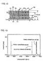
- the preferred arrangement of the piezoelectric thin-films 1 through n is determined as shown in Fig. 4.
- the vibrator portion 10a is made to vibrate at an n th higher-order mode and is made up of n piezoelectric thin-film layers 1 through n.
- Each piezoelectric thin-film layer is located at a respective distance d from one side (the lower side in Fig. 1) of the vibrator portion 10a as measured in the thickness direction thereof.
- Neighboring piezoelectric thin-film layers 1 through n are preferably arranged so that the orientation axis (the C axis) is in the thickness direction of the vibrator portion 10a when the piezoelectric materials zinc oxide.
- the polarization direction is made in the thickness direction.
- the polarization directions of adjacent piezoelectric thin-film layers 1 through n are selected such that they are polarized either in the same direction or in opposite directions from one another. In the case where adjacent piezoelectric thin-film layers 1 through n are polarized in the same direction, voltages are applied to adjacent piezoelectric thin-films 1 through n with opposite phases as each other. In the case where adjacent piezoelectric thin-films 1 through n are polarized in the opposite direction, voltages are applied to adjacent piezoelectric thin-films 1 through n with the same phase as each other. In both cases, the adjacent piezoelectric thin-films 1 through n are excited in opposite phases.
- piezoelectric thin-films which have temperature coefficient of the elastic constant which are opposite to one another.
- different materials of positive and negative temperature coefficients as in a group of ZnO (- 161 ppm/°C, LiNbO 3 (- 153 ppm/°C), and quartz (- 188 ppm/°C) on the one hand and a group of SiO 2 (+ 239 ppm/°C) and AlN(+ 100 ppm/°C) on the other. By doing so, the temperature characteristics of the frequency of the piezoelectric resonator is stabilized.
- the piezoelectric resonator When the piezoelectric resonator is made to, as shown in Fig. 4, the resonator is excited at a nth mode by applying voltages to the piezoelectric thin-films 1 through n as explained above.
- the piezoelectric thin-film layers 1 through n at the nodal points of the vibration and exciting the neighboring piezoelectric thin-film layers 1 through n in opposite phase, it is possible to increase the electromechanical coupling coefficient at the nth higher-order vibration mode and strongly excite the nth higher-order vibration mode.
- Waveform A shows the first (basic) vibration mode of a conventional piezoelectric resonator composed of one layer of piezoelectric thin-film 1.
- Waveforms B through E show the second through fifth higher-order vibration modes in the piezoelectric resonator according to the present invention where voltages of opposite phase are applied to the neighboring piezoelectric thin-films 1 through n.
- the thickness of the vibrator portion is set to be half of the resonance wavelength 2 of the first(basic) vibration mode.
- Figs. 6 and 9 show two piezoelectric resonators 20 having the same structure. However, the piezoelectric resonator 20 shown in Fig. 6 is driven so that the adjacent piezoelectric thin film layers are excited with the same phase, thereby constituting a comparative example. The piezoelectric resonator 20 shown in Fig. 9 is driven so that the adjacent piezoelectric thin film layers are excited with opposite in accordance with the preferred embodiments of the present invention.
- the vibrator portion 20a of this piezoelectric resonator 20 is composed of two layers of piezoelectric thin-films 1a and 2a and three layers of insulating thin films 13 which are alternately laminated to one another.
- ZnO is used for the piezoelectric thin-films 1a and 2a
- SiO 2 is used for the insulating thin films 12.
- the both of the ZnO layers have an orientation axis in the thickness direction of the piezoelectric vibrator portion.
- the thickness of the vibrator portion is 10 ⁇ m.
- the thickness of each of the piezoelectric thin-film layers 1a and 2a is 3 ⁇ m.
- the thickness of each of the insulating thin film layers 13 is 4/3 ⁇ m.
- the vibration generated at the piezoelectric thin-film layer 1a is propagated in the direction of the solid arrow toward the piezoelectric thin-film layer 2a along the excitation cosine curve shown by the solid line. Further, the vibration generated at the piezoelectric thin-film layer 2a is propagated in the direction of the broken line arrow toward the piezoelectric thin-film layer 1a along the excitation cosine curve shown in broken line.
- a resonance of the fundamental (first) vibration mode occurs around 250 MHz as shown in Fig. 8. Because mechanical vibrations of opposite phase are generated by the piezoelectric thin-film layers 1a and 2a in the second vibration mode, these vibrations cancel each other with the result that no response is brought around the frequency of the second vibration mode.
- a piezoelectric resonator 20 having the same construction as the piezoelectric resonator shown in Fig. 6, electric fields in opposite direction to each other are applied to the neighboring piezoelectric thin-film layers 1a and 2a as shown by the arrows in Fig. 9.
- the vibration generated by the piezoelectric thin-film layer 1a is propagated in the direction of the piezoelectric thin-film layer 2a on the excitation cosine curve shown by an arrow of solid line
- the vibration generated at the piezoelectric thin-film layer 2a is propagated in the direction of the piezoelectric thin-film layer 1a on the excitation cosine curve shown by an arrow of broken line.
- a resonance characteristic as shown in Fig. 11 can be obtained.
- a resonance based on the second vibration mode occurs around 580 MHz. This resonance occurs because the mechanical vibrations of the piezoelectric thin-film layers 1a and 2a become of the same phase and strengthen each other in the second vibration mode. In contrast, the responses due to the first vibration mode cancel each other to disappear or attenuate.
- the vibrator portion 30a of this piezoelectric resonator 30 is composed of three piezoelectric thin-film layers 1b through 3b and four insulating thin film layers 14 which are alternately laminated to one another.
- ZnO is used for the piezoelectric thin films of the piezoelectric thin-film layers 1b through 3b
- SiO 2 is used for the insulating thin film layers 14.
- the piezoelectric thin film layers (ZnO) of 1b through 3b have their orientation axis in the thickness direction.
- the thickness of the vibrator portion 30a is 10 ⁇ m.
- the thickness of the piezoelectric thin-film layers 1b through 3b are each 2 ⁇ m.
- Each of the insulating thin film layers 14 is 1 ⁇ m.
- the reason why the relationship of an even or odd multiple is not established between the frequency of the above first vibration mode and the frequency of the second vibration mode or third vibration mode is a composite construction of ZnO and SiO 2 and their different ratio of film thicknesses and velocity of sound.
Landscapes
- Physics & Mathematics (AREA)
- Acoustics & Sound (AREA)
- Engineering & Computer Science (AREA)
- Manufacturing & Machinery (AREA)
- Piezo-Electric Or Mechanical Vibrators, Or Delay Or Filter Circuits (AREA)
Abstract
Description
| Order | Formula | Calculation | Absolute Difference |
| First order | 5 | 5.4 | 0.4 |
| Second order | 2.5 | 2.43 | 0.07 |
| 7.5 | 7.15 | 0.35 | |
| Third order | 1.7 | 1.6 | 0.1 |
| 5 | 4.52 | 0.48 | |
| 8.3 | 7.86 | 0.44 | |
| Fourth order | 1.25 | 1.25 | 0 |
| 3.75 | 3.54 | 0.21 | |
| 6.25 | 5.91 | 0.34 | |
| 8.75 | 8.4 | 0.35 | |
| | 1 | 0.97 | 0.03 |
| 3 | 3 | 0 | |
| 5 | 5.02 | 0.02 | |
| 7 | 7.02 | 0.02 | |
| 9 | 9.03 | 0.03 |
Claims (32)
- A piezoelectric resonator using a thickness extensional vibration mode, the piezoelectric resonator comprising a vibrator portion (10a; 20a; 30a) made up of n layers of piezoelectric thin-film (1, 2, ..., n; 1a, 2a; 1b, 2b, 3b), n being an integer greater of equal to 2, each of the piezoelectric thin-film layers (1, ..., n; 1a, 2a; 1b - 3b) being separated by a respective insulating thin-film layer (12; 13; 14), the distance d of the nth piezoelectric thin-film layer (n) from a first side of the vibrator portion (10a; 20a; 30a), being determined by the formula
- A piezoelectric resonator as claimed in claim 1, wherein each of the piezoelectric thin-film layers (1, ..., n; 1a, 2a; 1b - 3b) comprises a generally planar piezoelectric thin-film having electrodes (e1, e2) formed on opposite sides thereof.
- A piezoelectric resonator as claimed in claim 2, wherein each of the piezoelectric thin-film layers (1, ..., n; 1a, 2a, 1b - 3b) and each of the insulating thin-film layers (12; 13; 14) are generally planar and extend parallel to one another.
- A piezoelectric resonator as claimed in claim 2 or 3, wherein the piezoelectric thin-films (1, ..., n; 1a, 2a; 1b - 3b) and the insulating thin film layers (12; 13; 14) are made up of materials having temperature coefficients of the elastic constant whose sign is opposite to one another.
- A piezoelectric resonator as claimed in any of claims 1 to 4, wherein adjacent piezoelectric thin-film layers (1, ..., n; 1a, 2a; 1b - 3b) are polarized in the same direction.
- A piezoelectric resonator as claimed in any of claims 1 to 4, wherein adjacent piezoelectric thin-films (1, ..., n; 1a, 2a; 1b - 3b) are polarized in opposite directions.
- A piezoelectric resonator as claimed in claim 1, wherein the thickness t is equal to one half of the wave length of the first resonance wavelength of the thickness extension vibration mode.
- The combination of a piezoelectric resonator and a voltage source, the combination comprising:a piezoelectric resonator using a thickness extensional vibration mode, the piezoelectric resonator comprising a vibrator portion (10a; 20a; 30a) made up of n layers of piezoelectric thin-film (1, ..., n; 1a, 2a; 1b - 3b), n being an integer greater of equal to 2, each of the piezoelectric thin-film layers (1, ..., n; 1a, 2a; 1b - 3b) being separated by a respective insulating thin-film layer (12; 13; 14); anda voltage source for applying alternating voltages to the piezoelectric resonator in such a manner that the predominant vibration mode excited in the piezoelectric resonator is a higher-order vibration mode.
- The combination according to claim 8, wherein the alternating voltages are independently applied to each of the piezoelectric thin-film layers (1, ..., n; 1a, 2a; 1b - 3b).
- The combination of claim 8 or 9, wherein the higher-order vibration mode is the nth vibration mode.
- The combination of claim 10, wherein the distance d of the nth piezoelectric thin-film layer (n) from a first side of the vibrator portion (10a; 20a; 30a) is determined by the formula
- The combination of claim 11, wherein each of the piezoelectric thin-film layers (1, ..., n; 1a, 2a; 1b - 3b) comprises a generally planar piezoelectric thin-film having electrodes (e1, e2) formed on opposite sides thereof.
- The combination of claim 12 wherein each of the piezoelectric thin-film layers (1, ..., n; 1a, 2a; 1b - 3b) and each of the insulating thin-film layers (12; 13; 14) are generally planar and extend parallel to one another.
- The combination of claim 13, wherein the piezoelectric thin-films (1, ..., n; 1a, 2a; 1b - 3b) and the insulating thin film layers (12; 13; 14) are made up of materials having temperature coefficients of the elastic constant whose sign is opposite to one another.
- The combination of any of claims 8 to 14, wherein adjacent piezoelectric thin-film layers (1, ..., n; 1a, 2a; 1b - 3b) are polarized in the same direction and the voltage source applies alternating voltages of the opposite phase to adjacent piezoelectric thin-film layers (1, ..., n; 1a, 2a; 1b - 3b).
- The combination of any of claims 8 to 14 wherein adjacent piezoelectric thin-film layers (1, ..., n; 1a, 2a; 1b - 3b) are polarized in opposite directions and the voltage source applies alternating voltages of the same phase to each of the piezoelectric thin-film layers (1, ..., n; 1a, 2a; 1b - 3b).
- The combination of any of claims 8 to 16, wherein the voltage source applies alternating voltages to the piezoelectric thin-film layers (1, ..., n; 1a, 2a; 1b - 3b) in such a manner that vibrations of opposite phase are induced in adjacent piezoelectric thin-film layers.
- The combination of any of claims 11 to 17, wherein the thickness t is equal to one half of the wave length of the first resonance wavelength of the thickness extension vibration mode.
- A method for exciting a piezoelectric resonator in a thickness extensional vibration mode, the piezoelectric resonator comprising a vibrator portion (10a; 20a; 30a) made up of n layers of piezoelectric thin-film (1, ..., n; 1a, 2a; 1b - 3b), n being an integer greater of equal to 2, each of the piezoelectric thin-film layers (1, ..., n; 1a, 2a; 1b - 3b) being separated by a respective insulating thin-film layer (12; 13; 14), the method comprising:applying alternating voltages to the piezoelectric thin film layers (1, ..., n; 1a, 2a; 1b - 3b) in such a manner that the predominant vibration mode excited in the piezoelectric resonator is a higher-order vibration mode.
- The method of claim 19, wherein the alternating voltages are independently applied to each of the piezoelectric thin-film layers (1, ..., n; 1a, 2a; 1b - 3b).
- The method of claim 19, wherein the higher-order vibration mode is the nth vibration mode.
- The method of claim 21, wherein the distance d of the nth piezoelectric thin-film layer (1, ..., n; 1a, 2a; 1b - 3b) from a first side of the vibrator portion is determined by the formula
- The method of claim 22, wherein each of the piezoelectric thin-film layers (1, ..., n; 1a, 2a; 1b - 3b) comprises a generally planar piezoelectric thin-film having electrodes (e1, e2) formed on opposite sides thereof.
- The method of claim 23 wherein each of the piezoelectric thin-film layers (1, ..., n; 1a, 2a; 1b - 3b) and each of the insulating thin-film layers (12; 13; 14) are generally planar and extend parallel to one another.
- The method of claim 24, wherein the piezoelectric thin-films (1, ..., n; 1a, 2a; 1b - 3b) and the insulating thin film layers (12; 13; 14) are made up of materials having temperature coefficients of the elastic constant whose sign is opposite to one another.
- The method of any of claims 19 to 25, wherein adjacent piezoelectric thin-film layers (1, ..., n; 1a, 2a; 1b - 3b) are polarized in the same direction and alternating voltages of the opposite phase are applied to adjacent piezoelectric thin-film layers (1, ..., n; 1a, 2a; 1b - 3b).
- The method of any of claims 19 to 25, wherein adjacent piezoelectric thin-film layers (1, ..., n; 1a, 2a; 1b - 3b) are polarized in opposite directions and alternating voltages of the same phase are applied to each of the piezoelectric thin-film layers (1, ..., n; 1a, 2a; 1b - 3b).
- The method of any of claims 19 to 27, wherein alternating voltages are applied to the piezoelectric thin-film layers (1, ..., n; 1a, 2a; 1b - 3b) in such a manner that vibrations of opposite phase are induced in adjacent piezoelectric thin-film layers (1, ..., n; 1a, 2a; 1b - 3b).
- The method of any of claims 22 to 28, wherein the thickness t is equal to one half of the wave length of the first resonance wavelength of the thickness extension vibration mode.
- The piezoelectric vibrator according to any of claims 1 to 7, wherein the distance d of each piezoelectric thin-film layer (1, ..., n; 1a, 2a; 1b - 3b) from the first side of the vibrator portion (10a; 20a; 30a) is measured at the center of the piezoelectric thin-film layer (1, ..., n; 1a, 2a; 1b - 3b) in the thickness direction thereof.
- The combination of any of claims 11 to 18, wherein the distance d of each piezoelectric thin-film layer (1, ..., n; 1a, 2a; 1b - 3b) from the first side of the vibrator portion (10a; 20a; 30a) is measured at the center of the piezoelectric thin-film layer (1, ..., n; 1a, 2a; 1b - 3b) in the thickness direction thereof.
- The method of any of claims 20 to 29, wherein the distance d of each piezoelectric thin-film layer (1, ..., n; 1a, 2a; 1b - 3b) from the first side of the vibrator portion (10a; 20a; 30a) is measured at the center of the piezoelectric thin-film layer (1, ..., n; 1a, 2a; 1b - 3b) in the thickness direction thereof.
Applications Claiming Priority (2)
| Application Number | Priority Date | Filing Date | Title |
|---|---|---|---|
| JP11129999A JP3531522B2 (en) | 1999-04-19 | 1999-04-19 | Piezoelectric resonator |
| JP11129999 | 1999-04-19 |
Publications (3)
| Publication Number | Publication Date |
|---|---|
| EP1047189A2 true EP1047189A2 (en) | 2000-10-25 |
| EP1047189A3 EP1047189A3 (en) | 2001-09-19 |
| EP1047189B1 EP1047189B1 (en) | 2011-02-16 |
Family
ID=14557712
Family Applications (1)
| Application Number | Title | Priority Date | Filing Date |
|---|---|---|---|
| EP00108101A Expired - Lifetime EP1047189B1 (en) | 1999-04-19 | 2000-04-12 | Piezoelectric resonator |
Country Status (5)
| Country | Link |
|---|---|
| US (1) | US6437482B1 (en) |
| EP (1) | EP1047189B1 (en) |
| JP (1) | JP3531522B2 (en) |
| KR (1) | KR100503664B1 (en) |
| DE (1) | DE60045628D1 (en) |
Cited By (29)
| Publication number | Priority date | Publication date | Assignee | Title |
|---|---|---|---|---|
| EP1100196A3 (en) * | 1999-11-11 | 2002-02-13 | Murata Manufacturing Co., Ltd. | Piezoelectric Resonator |
| WO2003032486A1 (en) * | 2001-10-08 | 2003-04-17 | Infineon Technologies Ag | Baw resonator |
| WO2003043188A1 (en) * | 2001-11-14 | 2003-05-22 | Infineon Technologies Ag | Passivated baw resonator and baw filter |
| US7242270B2 (en) | 2003-10-30 | 2007-07-10 | Avago Technologies Wireless Ip (Singapore) Pte. Ltd. | Decoupled stacked bulk acoustic resonator-based band-pass filter |
| GB2423428B (en) * | 2003-10-30 | 2007-09-05 | Agilent Technologies Inc | Temperature-compensated film bulk acoustic resonator (fbar) devices |
| US7367095B2 (en) | 2003-10-30 | 2008-05-06 | Avago Technologies General Ip Pte Ltd | Method of making an acoustically coupled transformer |
| US7369013B2 (en) | 2005-04-06 | 2008-05-06 | Avago Technologies Wireless Ip Pte Ltd | Acoustic resonator performance enhancement using filled recessed region |
| US7388454B2 (en) | 2004-10-01 | 2008-06-17 | Avago Technologies Wireless Ip Pte Ltd | Acoustic resonator performance enhancement using alternating frame structure |
| US7388455B2 (en) | 2003-10-30 | 2008-06-17 | Avago Technologies Wireless Ip Pte Ltd | Film acoustically-coupled transformer with increased common mode rejection |
| US7391286B2 (en) | 2005-10-06 | 2008-06-24 | Avago Wireless Ip Pte Ltd | Impedance matching and parasitic capacitor resonance of FBAR resonators and coupled filters |
| US7423503B2 (en) | 2005-10-18 | 2008-09-09 | Avago Technologies Wireless Ip (Singapore) Pte. Ltd. | Acoustic galvanic isolator incorporating film acoustically-coupled transformer |
| US7424772B2 (en) | 2003-10-30 | 2008-09-16 | Avago Technologies Wireless Ip (Singapore) Pte. Ltd. | Stacked bulk acoustic resonator band-pass filter with controllable pass bandwidth |
| US7427819B2 (en) | 2005-03-04 | 2008-09-23 | Avago Wireless Ip Pte Ltd | Film-bulk acoustic wave resonator with motion plate and method |
| US7436269B2 (en) | 2005-04-18 | 2008-10-14 | Avago Technologies Wireless Ip (Singapore) Pte. Ltd. | Acoustically coupled resonators and method of making the same |
| US7443269B2 (en) | 2005-07-27 | 2008-10-28 | Avago Technologies General Ip (Singapore) Pte. Ltd. | Method and apparatus for selectively blocking radio frequency (RF) signals in a radio frequency (RF) switching circuit |
| US7463499B2 (en) | 2005-10-31 | 2008-12-09 | Avago Technologies General Ip (Singapore) Pte Ltd. | AC-DC power converter |
| US7508286B2 (en) | 2006-09-28 | 2009-03-24 | Avago Technologies Wireless Ip (Singapore) Pte. Ltd. | HBAR oscillator and method of manufacture |
| US7561009B2 (en) | 2005-11-30 | 2009-07-14 | Avago Technologies General Ip (Singapore) Pte. Ltd. | Film bulk acoustic resonator (FBAR) devices with temperature compensation |
| US7615833B2 (en) | 2004-07-13 | 2009-11-10 | Avago Technologies Wireless Ip (Singapore) Pte. Ltd. | Film bulk acoustic resonator package and method of fabricating same |
| US7629865B2 (en) | 2006-05-31 | 2009-12-08 | Avago Technologies Wireless Ip (Singapore) Pte. Ltd. | Piezoelectric resonator structures and electrical filters |
| US7675390B2 (en) | 2005-10-18 | 2010-03-09 | Avago Technologies Wireless Ip (Singapore) Pte. Ltd. | Acoustic galvanic isolator incorporating single decoupled stacked bulk acoustic resonator |
| US7732977B2 (en) | 2008-04-30 | 2010-06-08 | Avago Technologies Wireless Ip (Singapore) | Transceiver circuit for film bulk acoustic resonator (FBAR) transducers |
| US7746677B2 (en) | 2006-03-09 | 2010-06-29 | Avago Technologies Wireless Ip (Singapore) Pte. Ltd. | AC-DC converter circuit and power supply |
| US7791434B2 (en) | 2004-12-22 | 2010-09-07 | Avago Technologies Wireless Ip (Singapore) Pte. Ltd. | Acoustic resonator performance enhancement using selective metal etch and having a trench in the piezoelectric |
| US7791435B2 (en) | 2007-09-28 | 2010-09-07 | Avago Technologies Wireless Ip (Singapore) Pte. Ltd. | Single stack coupled resonators having differential output |
| US7802349B2 (en) | 2003-03-07 | 2010-09-28 | Avago Technologies Wireless Ip (Singapore) Pte. Ltd. | Manufacturing process for thin film bulk acoustic resonator (FBAR) filters |
| US7868522B2 (en) | 2005-09-09 | 2011-01-11 | Avago Technologies Wireless Ip (Singapore) Pte. Ltd. | Adjusted frequency temperature coefficient resonator |
| EP1911157B1 (en) * | 2005-07-29 | 2013-05-22 | Compagnie Generale Des Etablissements Michelin | Hybrid resonant structure for verifying parameters of a tyre |
| US9859205B2 (en) | 2011-01-31 | 2018-01-02 | Avago Technologies General Ip (Singapore) Pte. Ltd. | Semiconductor device having an airbridge and method of fabricating the same |
Families Citing this family (37)
| Publication number | Priority date | Publication date | Assignee | Title |
|---|---|---|---|---|
| JP3903842B2 (en) * | 2001-07-03 | 2007-04-11 | 株式会社村田製作所 | Piezoelectric resonator, filter and electronic communication device |
| US6936954B2 (en) * | 2001-08-29 | 2005-08-30 | Honeywell International Inc. | Bulk resonator |
| US6670866B2 (en) * | 2002-01-09 | 2003-12-30 | Nokia Corporation | Bulk acoustic wave resonator with two piezoelectric layers as balun in filters and duplexers |
| KR20030073842A (en) * | 2002-03-13 | 2003-09-19 | 엘지이노텍 주식회사 | Flim bulk acoustic resonator filter and manufacturing method for the same |
| US7362198B2 (en) | 2003-10-30 | 2008-04-22 | Avago Technologies Wireless Ip (Singapore) Pte. Ltd | Pass bandwidth control in decoupled stacked bulk acoustic resonator devices |
| JPWO2005107066A1 (en) | 2004-04-30 | 2008-03-21 | 株式会社村田製作所 | Piezoelectric thin film resonator |
| US8981876B2 (en) | 2004-11-15 | 2015-03-17 | Avago Technologies General Ip (Singapore) Pte. Ltd. | Piezoelectric resonator structures and electrical filters having frame elements |
| US7202560B2 (en) | 2004-12-15 | 2007-04-10 | Avago Technologies Wireless Ip (Singapore) Pte. Ltd. | Wafer bonding of micro-electro mechanical systems to active circuitry |
| JP2006203304A (en) * | 2005-01-18 | 2006-08-03 | Hitachi Media Electoronics Co Ltd | Piezoelectric thin film resonator, oscillator using the same, and semiconductor integrated circuit incorporating the same |
| US7934884B2 (en) * | 2005-04-27 | 2011-05-03 | Lockhart Industries, Inc. | Ring binder cover |
| US7737807B2 (en) | 2005-10-18 | 2010-06-15 | Avago Technologies Wireless Ip (Singapore) Pte. Ltd. | Acoustic galvanic isolator incorporating series-connected decoupled stacked bulk acoustic resonators |
| US7525398B2 (en) | 2005-10-18 | 2009-04-28 | Avago Technologies General Ip (Singapore) Pte. Ltd. | Acoustically communicating data signals across an electrical isolation barrier |
| US7425787B2 (en) | 2005-10-18 | 2008-09-16 | Avago Technologies Wireless Ip (Singapore) Pte. Ltd. | Acoustic galvanic isolator incorporating single insulated decoupled stacked bulk acoustic resonator with acoustically-resonant electrical insulator |
| KR100718095B1 (en) | 2005-12-19 | 2007-05-16 | 삼성전자주식회사 | Coupling Resonance Filter and its Manufacturing Method |
| US7612636B2 (en) | 2006-01-30 | 2009-11-03 | Avago Technologies Wireless Ip (Singapore) Pte. Ltd. | Impedance transforming bulk acoustic wave baluns |
| US7479685B2 (en) | 2006-03-10 | 2009-01-20 | Avago Technologies General Ip (Singapore) Pte. Ltd. | Electronic device on substrate with cavity and mitigated parasitic leakage path |
| US7515018B2 (en) | 2006-08-31 | 2009-04-07 | Martin Handtmann | Acoustic resonator |
| DE102007042663A1 (en) * | 2007-09-10 | 2009-03-12 | Krohne Ag | ultrasound probe |
| US7855618B2 (en) | 2008-04-30 | 2010-12-21 | Avago Technologies Wireless Ip (Singapore) Pte. Ltd. | Bulk acoustic resonator electrical impedance transformers |
| US8902023B2 (en) | 2009-06-24 | 2014-12-02 | Avago Technologies General Ip (Singapore) Pte. Ltd. | Acoustic resonator structure having an electrode with a cantilevered portion |
| US8248185B2 (en) | 2009-06-24 | 2012-08-21 | Avago Technologies Wireless Ip (Singapore) Pte. Ltd. | Acoustic resonator structure comprising a bridge |
| US8193877B2 (en) | 2009-11-30 | 2012-06-05 | Avago Technologies Wireless Ip (Singapore) Pte. Ltd. | Duplexer with negative phase shifting circuit |
| US8796904B2 (en) | 2011-10-31 | 2014-08-05 | Avago Technologies General Ip (Singapore) Pte. Ltd. | Bulk acoustic resonator comprising piezoelectric layer and inverse piezoelectric layer |
| US9243316B2 (en) | 2010-01-22 | 2016-01-26 | Avago Technologies General Ip (Singapore) Pte. Ltd. | Method of fabricating piezoelectric material with selected c-axis orientation |
| US9203374B2 (en) | 2011-02-28 | 2015-12-01 | Avago Technologies General Ip (Singapore) Pte. Ltd. | Film bulk acoustic resonator comprising a bridge |
| US9154112B2 (en) | 2011-02-28 | 2015-10-06 | Avago Technologies General Ip (Singapore) Pte. Ltd. | Coupled resonator filter comprising a bridge |
| US9083302B2 (en) | 2011-02-28 | 2015-07-14 | Avago Technologies General Ip (Singapore) Pte. Ltd. | Stacked bulk acoustic resonator comprising a bridge and an acoustic reflector along a perimeter of the resonator |
| US9048812B2 (en) | 2011-02-28 | 2015-06-02 | Avago Technologies General Ip (Singapore) Pte. Ltd. | Bulk acoustic wave resonator comprising bridge formed within piezoelectric layer |
| US9425764B2 (en) | 2012-10-25 | 2016-08-23 | Avago Technologies General Ip (Singapore) Pte. Ltd. | Accoustic resonator having composite electrodes with integrated lateral features |
| US9148117B2 (en) | 2011-02-28 | 2015-09-29 | Avago Technologies General Ip (Singapore) Pte. Ltd. | Coupled resonator filter comprising a bridge and frame elements |
| US9136818B2 (en) | 2011-02-28 | 2015-09-15 | Avago Technologies General Ip (Singapore) Pte. Ltd. | Stacked acoustic resonator comprising a bridge |
| US8575820B2 (en) | 2011-03-29 | 2013-11-05 | Avago Technologies General Ip (Singapore) Pte. Ltd. | Stacked bulk acoustic resonator |
| US9444426B2 (en) | 2012-10-25 | 2016-09-13 | Avago Technologies General Ip (Singapore) Pte. Ltd. | Accoustic resonator having integrated lateral feature and temperature compensation feature |
| US8350445B1 (en) | 2011-06-16 | 2013-01-08 | Avago Technologies Wireless Ip (Singapore) Pte. Ltd. | Bulk acoustic resonator comprising non-piezoelectric layer and bridge |
| US9406865B2 (en) * | 2011-08-19 | 2016-08-02 | Qualcomm Incorporated | Composite piezoelectric laterally vibrating resonator |
| US8922302B2 (en) | 2011-08-24 | 2014-12-30 | Avago Technologies General Ip (Singapore) Pte. Ltd. | Acoustic resonator formed on a pedestal |
| US20160352307A1 (en) | 2015-05-27 | 2016-12-01 | Murata Manufacturing Co., Ltd. | Mems resonator with high quality factor |
Family Cites Families (10)
| Publication number | Priority date | Publication date | Assignee | Title |
|---|---|---|---|---|
| GB1207974A (en) | 1966-11-17 | 1970-10-07 | Clevite Corp | Frequency selective apparatus including a piezoelectric device |
| JPS58137317A (en) * | 1982-02-09 | 1983-08-15 | Nec Corp | Thin-film piezoelectric compound oscillator |
| JPS6016010A (en) * | 1983-07-07 | 1985-01-26 | Nec Corp | Piezoelectric thin film composite oscillator |
| JPS60189307A (en) * | 1984-03-09 | 1985-09-26 | Toshiba Corp | Piezoelectric thin film resonator and its manufacture |
| JPS6367910A (en) | 1986-09-10 | 1988-03-26 | Fujitsu Ltd | Piezoelectric thin film resonator |
| US5075641A (en) * | 1990-12-04 | 1991-12-24 | Iowa State University Research Foundation, Inc. | High frequency oscillator comprising cointegrated thin film resonator and active device |
| US5231327A (en) | 1990-12-14 | 1993-07-27 | Tfr Technologies, Inc. | Optimized piezoelectric resonator-based networks |
| US5587620A (en) * | 1993-12-21 | 1996-12-24 | Hewlett-Packard Company | Tunable thin film acoustic resonators and method for making the same |
| JP3371050B2 (en) | 1995-10-27 | 2003-01-27 | 三菱電機株式会社 | Thin film piezoelectric element |
| US6140740A (en) * | 1997-12-30 | 2000-10-31 | Remon Medical Technologies, Ltd. | Piezoelectric transducer |
-
1999
- 1999-04-19 JP JP11129999A patent/JP3531522B2/en not_active Expired - Fee Related
-
2000
- 2000-04-11 US US09/547,193 patent/US6437482B1/en not_active Expired - Lifetime
- 2000-04-12 EP EP00108101A patent/EP1047189B1/en not_active Expired - Lifetime
- 2000-04-12 DE DE60045628T patent/DE60045628D1/en not_active Expired - Lifetime
- 2000-04-18 KR KR10-2000-0020336A patent/KR100503664B1/en not_active Expired - Lifetime
Cited By (32)
| Publication number | Priority date | Publication date | Assignee | Title |
|---|---|---|---|---|
| EP1100196A3 (en) * | 1999-11-11 | 2002-02-13 | Murata Manufacturing Co., Ltd. | Piezoelectric Resonator |
| US6441539B1 (en) | 1999-11-11 | 2002-08-27 | Murata Manufacturing Co., Ltd. | Piezoelectric resonator |
| WO2003032486A1 (en) * | 2001-10-08 | 2003-04-17 | Infineon Technologies Ag | Baw resonator |
| US6975183B2 (en) | 2001-10-08 | 2005-12-13 | Infineon Technologies Ag | BAW resonator having piezoelectric layers oriented in opposed directions |
| WO2003043188A1 (en) * | 2001-11-14 | 2003-05-22 | Infineon Technologies Ag | Passivated baw resonator and baw filter |
| US7802349B2 (en) | 2003-03-07 | 2010-09-28 | Avago Technologies Wireless Ip (Singapore) Pte. Ltd. | Manufacturing process for thin film bulk acoustic resonator (FBAR) filters |
| GB2423428B (en) * | 2003-10-30 | 2007-09-05 | Agilent Technologies Inc | Temperature-compensated film bulk acoustic resonator (fbar) devices |
| US7367095B2 (en) | 2003-10-30 | 2008-05-06 | Avago Technologies General Ip Pte Ltd | Method of making an acoustically coupled transformer |
| US7388455B2 (en) | 2003-10-30 | 2008-06-17 | Avago Technologies Wireless Ip Pte Ltd | Film acoustically-coupled transformer with increased common mode rejection |
| US7242270B2 (en) | 2003-10-30 | 2007-07-10 | Avago Technologies Wireless Ip (Singapore) Pte. Ltd. | Decoupled stacked bulk acoustic resonator-based band-pass filter |
| US7424772B2 (en) | 2003-10-30 | 2008-09-16 | Avago Technologies Wireless Ip (Singapore) Pte. Ltd. | Stacked bulk acoustic resonator band-pass filter with controllable pass bandwidth |
| US7615833B2 (en) | 2004-07-13 | 2009-11-10 | Avago Technologies Wireless Ip (Singapore) Pte. Ltd. | Film bulk acoustic resonator package and method of fabricating same |
| US7714684B2 (en) | 2004-10-01 | 2010-05-11 | Avago Technologies Wireless Ip (Singapore) Pte. Ltd. | Acoustic resonator performance enhancement using alternating frame structure |
| US7388454B2 (en) | 2004-10-01 | 2008-06-17 | Avago Technologies Wireless Ip Pte Ltd | Acoustic resonator performance enhancement using alternating frame structure |
| US7791434B2 (en) | 2004-12-22 | 2010-09-07 | Avago Technologies Wireless Ip (Singapore) Pte. Ltd. | Acoustic resonator performance enhancement using selective metal etch and having a trench in the piezoelectric |
| US7427819B2 (en) | 2005-03-04 | 2008-09-23 | Avago Wireless Ip Pte Ltd | Film-bulk acoustic wave resonator with motion plate and method |
| US7369013B2 (en) | 2005-04-06 | 2008-05-06 | Avago Technologies Wireless Ip Pte Ltd | Acoustic resonator performance enhancement using filled recessed region |
| US7436269B2 (en) | 2005-04-18 | 2008-10-14 | Avago Technologies Wireless Ip (Singapore) Pte. Ltd. | Acoustically coupled resonators and method of making the same |
| US7443269B2 (en) | 2005-07-27 | 2008-10-28 | Avago Technologies General Ip (Singapore) Pte. Ltd. | Method and apparatus for selectively blocking radio frequency (RF) signals in a radio frequency (RF) switching circuit |
| EP1911157B1 (en) * | 2005-07-29 | 2013-05-22 | Compagnie Generale Des Etablissements Michelin | Hybrid resonant structure for verifying parameters of a tyre |
| US7868522B2 (en) | 2005-09-09 | 2011-01-11 | Avago Technologies Wireless Ip (Singapore) Pte. Ltd. | Adjusted frequency temperature coefficient resonator |
| US7391286B2 (en) | 2005-10-06 | 2008-06-24 | Avago Wireless Ip Pte Ltd | Impedance matching and parasitic capacitor resonance of FBAR resonators and coupled filters |
| US7675390B2 (en) | 2005-10-18 | 2010-03-09 | Avago Technologies Wireless Ip (Singapore) Pte. Ltd. | Acoustic galvanic isolator incorporating single decoupled stacked bulk acoustic resonator |
| US7423503B2 (en) | 2005-10-18 | 2008-09-09 | Avago Technologies Wireless Ip (Singapore) Pte. Ltd. | Acoustic galvanic isolator incorporating film acoustically-coupled transformer |
| US7463499B2 (en) | 2005-10-31 | 2008-12-09 | Avago Technologies General Ip (Singapore) Pte Ltd. | AC-DC power converter |
| US7561009B2 (en) | 2005-11-30 | 2009-07-14 | Avago Technologies General Ip (Singapore) Pte. Ltd. | Film bulk acoustic resonator (FBAR) devices with temperature compensation |
| US7746677B2 (en) | 2006-03-09 | 2010-06-29 | Avago Technologies Wireless Ip (Singapore) Pte. Ltd. | AC-DC converter circuit and power supply |
| US7629865B2 (en) | 2006-05-31 | 2009-12-08 | Avago Technologies Wireless Ip (Singapore) Pte. Ltd. | Piezoelectric resonator structures and electrical filters |
| US7508286B2 (en) | 2006-09-28 | 2009-03-24 | Avago Technologies Wireless Ip (Singapore) Pte. Ltd. | HBAR oscillator and method of manufacture |
| US7791435B2 (en) | 2007-09-28 | 2010-09-07 | Avago Technologies Wireless Ip (Singapore) Pte. Ltd. | Single stack coupled resonators having differential output |
| US7732977B2 (en) | 2008-04-30 | 2010-06-08 | Avago Technologies Wireless Ip (Singapore) | Transceiver circuit for film bulk acoustic resonator (FBAR) transducers |
| US9859205B2 (en) | 2011-01-31 | 2018-01-02 | Avago Technologies General Ip (Singapore) Pte. Ltd. | Semiconductor device having an airbridge and method of fabricating the same |
Also Published As
| Publication number | Publication date |
|---|---|
| KR20000077037A (en) | 2000-12-26 |
| EP1047189B1 (en) | 2011-02-16 |
| KR100503664B1 (en) | 2005-08-19 |
| JP2000307377A (en) | 2000-11-02 |
| EP1047189A3 (en) | 2001-09-19 |
| DE60045628D1 (en) | 2011-03-31 |
| JP3531522B2 (en) | 2004-05-31 |
| US6437482B1 (en) | 2002-08-20 |
Similar Documents
| Publication | Publication Date | Title |
|---|---|---|
| US6437482B1 (en) | Piezoelectric resonator | |
| US7414349B2 (en) | Piezoelectric vibrator, filter using the same and its adjusting method | |
| EP1170862B1 (en) | Piezoelectric resonator and piezoelectric filter using the same | |
| US9172351B2 (en) | Piezoelectric resonator having electrode fingers with electrode patches | |
| JP4820037B2 (en) | Interface acoustic filter, especially for wireless connection | |
| JP3514224B2 (en) | Piezoelectric resonator, filter and electronic device | |
| US20110304243A1 (en) | Thin-Film Piezoelectric Acoustic Wave Resonator and High-Frequency Filter | |
| JP2007036915A (en) | High-order mode thin film resonator | |
| CN102057570A (en) | HBAR resonators with high temperature stability | |
| JP3860695B2 (en) | Piezoelectric resonator and filter | |
| JP3979073B2 (en) | Piezoelectric resonator, piezoelectric filter and duplexer | |
| Plessky et al. | 3 rd type of FBARs? | |
| JPH0396005A (en) | Piezoelectric thin film resonator | |
| JP3723697B2 (en) | Piezoelectric resonator | |
| JPS60142607A (en) | Piezoelectric thin film composite oscillator | |
| WO2023236332A1 (en) | Plate mode resonator device | |
| JP7850819B2 (en) | Acoustic resonator rigidly mounted on a high acoustic velocity substrate | |
| KR100602907B1 (en) | Composite vibration device | |
| JP4339604B2 (en) | Piezoelectric thin film element | |
| JP4693407B2 (en) | Piezoelectric thin film device and manufacturing method thereof | |
| JPH10215140A (en) | Piezoelectric resonator and electronic component using the resonator | |
| JP2002009579A (en) | Piezo electric resonator and piezoelectric filter using the same | |
| JP4693406B2 (en) | Piezoelectric thin film device and manufacturing method thereof | |
| JP2009065513A (en) | Piezoelectric thin film resonator and piezoelectric resonant component with the same | |
| JP3937921B2 (en) | Composite material vibration device |
Legal Events
| Date | Code | Title | Description |
|---|---|---|---|
| PUAI | Public reference made under article 153(3) epc to a published international application that has entered the european phase |
Free format text: ORIGINAL CODE: 0009012 |
|
| 17P | Request for examination filed |
Effective date: 20000412 |
|
| AK | Designated contracting states |
Kind code of ref document: A2 Designated state(s): DE FR GB Kind code of ref document: A2 Designated state(s): AT BE CH CY DE DK ES FI FR GB GR IE IT LI LU MC NL PT SE |
|
| AX | Request for extension of the european patent |
Free format text: AL;LT;LV;MK;RO;SI |
|
| PUAL | Search report despatched |
Free format text: ORIGINAL CODE: 0009013 |
|
| AK | Designated contracting states |
Kind code of ref document: A3 Designated state(s): AT BE CH CY DE DK ES FI FR GB GR IE IT LI LU MC NL PT SE |
|
| AX | Request for extension of the european patent |
Free format text: AL;LT;LV;MK;RO;SI |
|
| AKX | Designation fees paid |
Free format text: DE FR GB |
|
| RAP1 | Party data changed (applicant data changed or rights of an application transferred) |
Owner name: MURATA MANUFACTURING CO., LTD. |
|
| 17Q | First examination report despatched |
Effective date: 20071115 |
|
| GRAP | Despatch of communication of intention to grant a patent |
Free format text: ORIGINAL CODE: EPIDOSNIGR1 |
|
| GRAS | Grant fee paid |
Free format text: ORIGINAL CODE: EPIDOSNIGR3 |
|
| GRAA | (expected) grant |
Free format text: ORIGINAL CODE: 0009210 |
|
| AK | Designated contracting states |
Kind code of ref document: B1 Designated state(s): DE FR GB |
|
| REG | Reference to a national code |
Ref country code: GB Ref legal event code: FG4D |
|
| REF | Corresponds to: |
Ref document number: 60045628 Country of ref document: DE Date of ref document: 20110331 Kind code of ref document: P |
|
| REG | Reference to a national code |
Ref country code: DE Ref legal event code: R096 Ref document number: 60045628 Country of ref document: DE Effective date: 20110331 |
|
| PLBE | No opposition filed within time limit |
Free format text: ORIGINAL CODE: 0009261 |
|
| STAA | Information on the status of an ep patent application or granted ep patent |
Free format text: STATUS: NO OPPOSITION FILED WITHIN TIME LIMIT |
|
| REG | Reference to a national code |
Ref country code: FR Ref legal event code: ST Effective date: 20111230 |
|
| 26N | No opposition filed |
Effective date: 20111117 |
|
| GBPC | Gb: european patent ceased through non-payment of renewal fee |
Effective date: 20110516 |
|
| PG25 | Lapsed in a contracting state [announced via postgrant information from national office to epo] |
Ref country code: FR Free format text: LAPSE BECAUSE OF NON-PAYMENT OF DUE FEES Effective date: 20110502 |
|
| REG | Reference to a national code |
Ref country code: DE Ref legal event code: R097 Ref document number: 60045628 Country of ref document: DE Effective date: 20111117 |
|
| PG25 | Lapsed in a contracting state [announced via postgrant information from national office to epo] |
Ref country code: GB Free format text: LAPSE BECAUSE OF NON-PAYMENT OF DUE FEES Effective date: 20110516 |
|
| PGFP | Annual fee paid to national office [announced via postgrant information from national office to epo] |
Ref country code: DE Payment date: 20190418 Year of fee payment: 20 |
|
| REG | Reference to a national code |
Ref country code: DE Ref legal event code: R071 Ref document number: 60045628 Country of ref document: DE |