EP1045453A2 - LED array PCB with adhesive rod lens - Google Patents
LED array PCB with adhesive rod lens Download PDFInfo
- Publication number
- EP1045453A2 EP1045453A2 EP00301862A EP00301862A EP1045453A2 EP 1045453 A2 EP1045453 A2 EP 1045453A2 EP 00301862 A EP00301862 A EP 00301862A EP 00301862 A EP00301862 A EP 00301862A EP 1045453 A2 EP1045453 A2 EP 1045453A2
- Authority
- EP
- European Patent Office
- Prior art keywords
- lens
- light
- adhesive
- board
- collection lens
- Prior art date
- Legal status (The legal status is an assumption and is not a legal conclusion. Google has not performed a legal analysis and makes no representation as to the accuracy of the status listed.)
- Granted
Links
Images

Classifications
-
- G—PHYSICS
- G02—OPTICS
- G02B—OPTICAL ELEMENTS, SYSTEMS OR APPARATUS
- G02B3/00—Simple or compound lenses
- G02B3/02—Simple or compound lenses with non-spherical faces
- G02B3/06—Simple or compound lenses with non-spherical faces with cylindrical or toric faces
-
- B—PERFORMING OPERATIONS; TRANSPORTING
- B29—WORKING OF PLASTICS; WORKING OF SUBSTANCES IN A PLASTIC STATE IN GENERAL
- B29D—PRODUCING PARTICULAR ARTICLES FROM PLASTICS OR FROM SUBSTANCES IN A PLASTIC STATE
- B29D11/00—Producing optical elements, e.g. lenses or prisms
- B29D11/00009—Production of simple or compound lenses
- B29D11/00365—Production of microlenses
-
- G—PHYSICS
- G02—OPTICS
- G02B—OPTICAL ELEMENTS, SYSTEMS OR APPARATUS
- G02B3/00—Simple or compound lenses
-
- G—PHYSICS
- G02—OPTICS
- G02B—OPTICAL ELEMENTS, SYSTEMS OR APPARATUS
- G02B3/00—Simple or compound lenses
- G02B3/0006—Arrays
- G02B3/0037—Arrays characterized by the distribution or form of lenses
- G02B3/005—Arrays characterized by the distribution or form of lenses arranged along a single direction only, e.g. lenticular sheets
-
- H—ELECTRICITY
- H10—SEMICONDUCTOR DEVICES; ELECTRIC SOLID-STATE DEVICES NOT OTHERWISE PROVIDED FOR
- H10W—GENERIC PACKAGES, INTERCONNECTIONS, CONNECTORS OR OTHER CONSTRUCTIONAL DETAILS OF DEVICES COVERED BY CLASS H10
- H10W90/00—Package configurations
-
- H—ELECTRICITY
- H10—SEMICONDUCTOR DEVICES; ELECTRIC SOLID-STATE DEVICES NOT OTHERWISE PROVIDED FOR
- H10H—INORGANIC LIGHT-EMITTING SEMICONDUCTOR DEVICES HAVING POTENTIAL BARRIERS
- H10H20/00—Individual inorganic light-emitting semiconductor devices having potential barriers, e.g. light-emitting diodes [LED]
- H10H20/80—Constructional details
- H10H20/83—Electrodes
- H10H20/832—Electrodes characterised by their material
-
- H—ELECTRICITY
- H10—SEMICONDUCTOR DEVICES; ELECTRIC SOLID-STATE DEVICES NOT OTHERWISE PROVIDED FOR
- H10H—INORGANIC LIGHT-EMITTING SEMICONDUCTOR DEVICES HAVING POTENTIAL BARRIERS
- H10H20/00—Individual inorganic light-emitting semiconductor devices having potential barriers, e.g. light-emitting diodes [LED]
- H10H20/80—Constructional details
- H10H20/85—Packages
- H10H20/852—Encapsulations
- H10H20/853—Encapsulations characterised by their shape
Definitions
- the light used to illuminate the target area is typically provided by light emitting diodes (LEDs). As shown in FIGURE 5, the light emitted from a LED 50 is spread over a large area. The light is emitted at a broad angle, with the half power point 52,53 being 80 degrees from the vertical axis 51.
- LEDs light emitting diodes
- an LED 61 includes collection lens 63 to collect and focus the light onto target area 31.
- LED 61 typically comprises a plurality of LEDs arranged in a single column array, and that lens 63 is a cylindrical lens.
- lens 33 is the SELFOC lens array from NSG.
- the lens 63 is typically an extruded or injection molded plastic lens, e.g. polycarbonate or acrylic.
- the light reflected from the surface 31 is captured by lens system 33 and focused onto detector 34.
- FIGURE 7 depicts an alternative LED arrangement 71 that uses reflecting optics 72 to reflect the light onto the target area in place of the refracting lens 63 of FIGURE 6.
- the light reflected from the surface 31 is captured by lens system 33 and focused onto detector 34.
- FIGURES 6 and 7 are expensive in terms of manufacturing, as each requires additional tooling to attach the lens or reflector to the LED board. Moreover, the lens and reflectors are additional parts which increase cost. Furthermore, note that the lens 63 requires lens mount 62 to attach the lens 63 to the LED 61. This lens mount adds a space requirement to the scan system, and in smaller systems such as a hand-held scanner space is expensive. Also the arrangement of FIGURE 7 is also costly in terms of space. For this arrangement to be effective, the trough formed by the reflector 72 must be deep, and thus reflector 72 protrudes from the LED board. Thus, the LED board 81 arrangement shown in FIGURE 8 is typically used.
- LED board 81 there is no light collection optics, instead a bare LED is used to illuminate the target area 31.
- the light reflected from the surface 31 is captured by lens system 33 and focused into detector 34.
- most of the light produced by LED board 81 is wasted, specifically only about .1% of the light is used and about 99.9% of the light is wasted.
- the optical adhesive is dispensed to cover the LED array. As the adhesive is dispensed, it is formed into the shape of a lens. The adhesive is then cured, and a lens is formed that covers the LED array. A lens shape is formed by the act of dispensing. The combination of gravity, viscosity characteristics of the adhesive, and surface tension characteristics of the adhesive co-act to form the lens shape. Alternatively, a lens form or mold can be used to provide better and more uniform lens shape to the adhesive.
- the LED array is located on a small PC board that is approximately 5 inches long by 1/4 inch wide.
- the LED array is comprised of 18 LEDs evenly spaced in one column on the PC board.
- the optical adhesive is then dispensed over the LEDs as a long rope of adhesive. Gravity, viscosity, and surface tension cause the adhesive to settle around the LEDs and retain a curved shape.
- the adhesive forms an approximately cylindrical lens over the LEDs.
- the adhesive is then either cured with heat or UV light. Note that the lens formed in this manner is not an accurate lens, as the lens will have irregularities in the lens shape, Moreover, and the shape will not be uniform over the length of the lens, when compared with a standard cylindrical lens.
- the inventive lens does not require the additional manufacturing costs of the prior art lens, nor does the inventive lens require the space of the prior art lens, as the inventive lens is integral with the LED array. Moreover, the inventive lens collects light that is emitted by the LEDs at extreme angles and directs the light to the scan location, and thus provides more light than the prior art arrangement of not using a lens.
- the lens is integral with the LEDs, and thus does not require attachment to the LED board.
- the invention is inexpensive as the adhesive has a low cost, and additional tooling and/or elements are not required to secure the lens to the array.
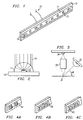
- FIGURE 1 depicts an isometric view of the inventive lens 11 attached to a printed circuit (PC) board 12 that includes a plurality of light emitting diodes (LEDs) 13 formed in an array 14.
- PC printed circuit
- LEDs light emitting diodes
- the board includes connections 15 to power the PC board 12.
- the lens 11 is formed by pumping an optical adhesive through a needle directly onto the board 12. The amount of adhesive dispensed determines the size of the lens.
- the surface tension and viscosity characteristics of the adhesive, as well as the effects of gravity, determine the shape of the lens 11. These characteristics and the effects of gravity co-act to form the crown or cylindrical shape of the lens 11.
- lens After dispensing, lens must be cured, either via heat or ultraviolet (UV) light, to prevent slumping or loss of curvature. Note that curing may not immediately occur after dispensing, depending on the viscosity of the adhesive, it might take some time for the lens shape to form, thus curing takes place after the shape has been formed. Thus, the lens is either passed beneath a UV light or processed through an oven. The overall operation is relatively short, perhaps approximately 10 seconds to dispense, and approximately 30 seconds for UV cure or 30-120 minutes for heat cure.
- UV ultraviolet
- lens 11 does provide reasonable light collection results, and it is also very quick and inexpensive.
- lens 11 also encapsulates and protects the LEDs 13.
- the board may be inverted during or subsequent to the dispensing of the adhesive. The inversion would cause gravity to assist in maintaining curvature of the adhesive.
- lens 11 collects light, including light 21 that is emitted from diode 13 at a large solid angle 21. This light is then delivered to the target area, and is used for illumination of scan target 31, as shown in FIGURE 3.
- the inventive lens and PC board 32 is mounted at approximately 45 degrees with respect to and approximately .16 inches (or about 4mm) from the scan target surface 31.
- the light reflected from the surface 31 is captured by lens system 33 and focused onto detector 34.
- lens 32 does not have to be capable of image quality light delivery, i.e. lens 32 may by a non-imaging lens, as lens 32 is intended to provide more light to surface 31.
- the adhesive materials contemplated for use as lens 11 include UV15-7TK1A, UV15X-5, and Sil 410, which are UV cured materials produced by Master Bond, as well as PT1002A/B, which is a heat cured material produced by Pacific Polytech, Inc. Of these materials, UV15 has been shown to perform the best. However, other materials may be used, such as epoxy, urethane, or acrylic, so long as the material has sufficient optical properties to transmit and refract light, at the correct wavelength in the visible range of the spectrum, and sufficient adhesive properties to adhere to the PC board 12. Note that the lens 11 is depicted and described in connection with LEDs, however lens 11 can be used with other elements for other systems, particularly where ever a integral lens with less than perfect optical characteristics can be used.
- An alternative lens 11 may be formed using a lens form or mold that has the desired shape.
- a cylindrical lens form can be applied to the adhesive material.
- the form may be pressed onto the PC board 12 or the board 12 may be moved through the form.
- the form would be coated with a non-stick material such as Teflon to prevent the adhesive from sticking to the form.
- Teflon a non-stick material
- the form would ensure that the lens 11 has an optically correct curvature.
- the form could be incorporated with the curing system, such that the proper shape is maintained during curing. Note that this system would require more tooling and expense than the simpler system described above, but would produce lenses with accurate and uniform shapes, whereby the lenses would be image capable.
- FIGURE 4A depicts lens 41 with a plurality of spherical lenses. Note that this lens arrangement will result in more light, it will by extremely non-uniform.
- the spherical lenses are formed via a lens mold that is pressed onto the adhesive on board 12. The shape and size of the spherical lenses would be selected to concentrate light onto the target area. Note that aspherical lenses may be used to collect more of the off-axis light emitted from the led. Further note that other lens shapes may be used, including cylindrical lense 42 as shown in FIGURE 4B. Still further note that a non-lens shape may be pressed onto the adhesive, so long as the light modifier formed collects and bends light. For example, a grating may be formed in the adhesive, which may then collect and focus the light onto the target area.
- each individual LED 13 comprises a wire frame with semiconductor material that is encased in an epoxy cube. Instead of encasing the LED in a cube, the LED wire frame would be encased in a lens. Thus, each individual LED wire frame would be placed into a mold that has a lens shape and cured. This would yield LEDS with individual, integral lenses 43, as shown in FIGURE 4C. Note that a plurality of LED wire frames could be placed into a larger lens mold to form a single lens array, e.g. as shown in FIGURE 1.
Landscapes
- Physics & Mathematics (AREA)
- General Physics & Mathematics (AREA)
- Optics & Photonics (AREA)
- Engineering & Computer Science (AREA)
- Ophthalmology & Optometry (AREA)
- Manufacturing & Machinery (AREA)
- Health & Medical Sciences (AREA)
- Mechanical Engineering (AREA)
- Facsimile Heads (AREA)
- Led Device Packages (AREA)
- Facsimile Scanning Arrangements (AREA)
- Led Devices (AREA)
- Light Sources And Details Of Projection-Printing Devices (AREA)
- Image Input (AREA)
- Printers Or Recording Devices Using Electromagnetic And Radiation Means (AREA)
Abstract
Description
Claims (10)
- A method for forming a light collection lens 11 on a board 12 comprising the steps of:dispensing an optical adhesive onto the board;forming a lens shape with the adhesive; andcuring the adhesive in the lens shape to form the light collection lens.
- The method of claim 1, wherein the board is a printed circuit board 12 that includes a plurality of light emitting diodes (LEDs) 13 arranged in an array 14, and the step of dispensing comprises the step of:dispensing the adhesive onto the array.
- The method of claim 2, wherein the step of forming comprises the step of:molding the adhesive into the lens shape with a lens mold.
- The method of claim 2, wherein the step of forming comprises the step of:maintaining the lens shape via the surface tension characteristic of the adhesive.
- The method of claim 1, wherein the step of curing comprises the step of:heating the adhesive to a predetermined temperature for a predetermined length of time.
- The method of claim 1, wherein the step of curing comprises the step of:exposing the adhesive to a predetermined wavelength of light for a predetermined length of time.
- A light collection lens that is formed on a board 12, wherein the board includes at least one light producing element 13, the lens 11 comprising:a base portion that is fixedly attached to the board and conforms to the profile of the light producing element on the board; anda curved portion that is located adjacent to the base portion and refracts a portion of the light from the light producing element toward an optical axis;
wherein the base portion and the curved portion are formed from an optical adhesive. - The light collection lens of claim 14, wherein the board 12 is a printed circuit board and the at least one light producing element 11 is a plurality of light emitting diodes (LEDs) arranged in an array 14.
- The light collection lens of claim 14, wherein the light collection lens 11 is used in a scanning system.
- The light collection lens of claim 19, wherein the light collection lens 11 collects light 21 from the light producing element 13 and directs the light to a scan target 31.
Applications Claiming Priority (2)
| Application Number | Priority Date | Filing Date | Title |
|---|---|---|---|
| US290131 | 1999-04-12 | ||
| US09/290,131 US6188527B1 (en) | 1999-04-12 | 1999-04-12 | LED array PCB with adhesive rod lens |
Publications (3)
| Publication Number | Publication Date |
|---|---|
| EP1045453A2 true EP1045453A2 (en) | 2000-10-18 |
| EP1045453A3 EP1045453A3 (en) | 2002-05-22 |
| EP1045453B1 EP1045453B1 (en) | 2005-06-29 |
Family
ID=23114668
Family Applications (1)
| Application Number | Title | Priority Date | Filing Date |
|---|---|---|---|
| EP00301862A Expired - Lifetime EP1045453B1 (en) | 1999-04-12 | 2000-03-07 | LED array PCB with adhesive rod lens |
Country Status (5)
| Country | Link |
|---|---|
| US (1) | US6188527B1 (en) |
| EP (1) | EP1045453B1 (en) |
| JP (1) | JP3507755B2 (en) |
| DE (1) | DE60021010T2 (en) |
| TW (1) | TWI235854B (en) |
Cited By (10)
| Publication number | Priority date | Publication date | Assignee | Title |
|---|---|---|---|---|
| EP1553049A3 (en) * | 2004-01-12 | 2005-08-10 | Agilent Technologies, Inc. | Method for manufacturing moulded micromechanical structures |
| DE102005011355A1 (en) * | 2005-03-04 | 2006-09-14 | Osa Opto Light Gmbh | Opto-electronic unit e.g. LED, for e.g. sensor, has cap made of material transparent for radiation and including optical absorbing layer that partially absorbs radiation such that radiation is suppressed in defined solid angle area |
| EP1724834A1 (en) * | 2005-05-16 | 2006-11-22 | Noctron Holding S.A. | Radiation generating device and night vision apparatus comprising such device |
| EP1860466A1 (en) * | 2006-05-23 | 2007-11-28 | STMicroelectronics (Rousset) SAS | Method of fabricating lenses, in particular for CMOS imaging devices. |
| WO2008145718A1 (en) * | 2007-06-01 | 2008-12-04 | Wacker Chemie Ag | Silicon moulded part comprising luminous bodies |
| EP2221891A1 (en) * | 2009-02-18 | 2010-08-25 | Everlight Electronics Co., Ltd. | Light emitting device |
| US8378358B2 (en) | 2009-02-18 | 2013-02-19 | Everlight Electronics Co., Ltd. | Light emitting device |
| US8405105B2 (en) | 2009-02-18 | 2013-03-26 | Everlight Electronics Co., Ltd. | Light emitting device |
| CN102141208B (en) * | 2010-02-03 | 2013-04-17 | 亿光电子工业股份有限公司 | lamps |
| US9069107B2 (en) | 2012-07-12 | 2015-06-30 | Schott Ag | Rod lens and methods for producing same |
Families Citing this family (64)
| Publication number | Priority date | Publication date | Assignee | Title |
|---|---|---|---|---|
| GB2357856B (en) * | 1999-12-29 | 2001-12-19 | Keymed | Annular light source in borescopes and endoscopes |
| EP1386357A1 (en) * | 2001-04-23 | 2004-02-04 | Plasma Ireland Limited | Illuminator |
| AT414165B (en) * | 2001-10-09 | 2006-09-15 | Gifas Electric Ges M B H | LAMP |
| US6857924B2 (en) * | 2002-06-03 | 2005-02-22 | Ta-Hao Fu | Method of producing an LED hose light |
| TW574822B (en) * | 2002-09-19 | 2004-02-01 | Veutron Corp | Light source module for scanning |
| JP2004170858A (en) * | 2002-11-22 | 2004-06-17 | Canon Inc | Image reading device |
| WO2005001944A1 (en) * | 2003-06-26 | 2005-01-06 | Nippon Sheet Glass Company, Limited | Lens-carrying light emitting element and production method therefor |
| US6921929B2 (en) * | 2003-06-27 | 2005-07-26 | Lockheed Martin Corporation | Light-emitting diode (LED) with amorphous fluoropolymer encapsulant and lens |
| US7683391B2 (en) * | 2004-05-26 | 2010-03-23 | Lockheed Martin Corporation | UV emitting LED having mesa structure |
| KR101070514B1 (en) * | 2004-05-31 | 2011-10-05 | 엘지디스플레이 주식회사 | Direct type back light assembly |
| JP4635494B2 (en) * | 2004-07-13 | 2011-02-23 | 富士ゼロックス株式会社 | Light emitting element with lens |
| US7482634B2 (en) * | 2004-09-24 | 2009-01-27 | Lockheed Martin Corporation | Monolithic array for solid state ultraviolet light emitters |
| US8109981B2 (en) | 2005-01-25 | 2012-02-07 | Valam Corporation | Optical therapies and devices |
| US8305225B2 (en) * | 2005-02-14 | 2012-11-06 | Truck-Lite Co., Llc | LED strip light lamp assembly |
| US20070208395A1 (en) * | 2005-10-05 | 2007-09-06 | Leclerc Norbert H | Phototherapy Device and Method of Providing Phototherapy to a Body Surface |
| US20070102718A1 (en) * | 2005-11-07 | 2007-05-10 | Akira Takekuma | Lens in light emitting device |
| US20070219600A1 (en) * | 2006-03-17 | 2007-09-20 | Michael Gertner | Devices and methods for targeted nasal phototherapy |
| KR100809263B1 (en) * | 2006-07-10 | 2008-02-29 | 삼성전기주식회사 | Direct type backlight device |
| US20080073028A1 (en) * | 2006-08-31 | 2008-03-27 | Frank Yu | Methods and apparatus to dispense adhesive for semiconductor packaging |
| KR100790741B1 (en) * | 2006-09-07 | 2008-01-02 | 삼성전기주식회사 | How to make lens for LED package |
| US20080074884A1 (en) * | 2006-09-25 | 2008-03-27 | Thye Linn Mok | Compact high-intensty LED-based light source and method for making the same |
| USD575246S1 (en) | 2006-11-15 | 2008-08-19 | Citizen Electronics Co., Ltd. | Light-emitting diode unit for illuminating an object |
| USD622676S1 (en) * | 2007-03-19 | 2010-08-31 | Nichia Corporation | LED display device |
| USD565515S1 (en) * | 2007-04-18 | 2008-04-01 | Edison Opto Corporation | Light emitting diode assembly for linear illumination |
| US7766536B2 (en) * | 2008-02-15 | 2010-08-03 | Lunera Lighting, Inc. | LED light fixture |
| TWD130494S1 (en) * | 2008-02-29 | 2009-08-21 | 先進開發光電股份有限公司 | Led module |
| USD616383S1 (en) * | 2008-09-03 | 2010-05-25 | Lunera Lighting, Inc. | LED module |
| USD619109S1 (en) * | 2008-09-03 | 2010-07-06 | Lunera Lighting, Inc. | LED module |
| USD623149S1 (en) * | 2008-09-03 | 2010-09-07 | Lunera Lighting, Inc. | LED module |
| TWI364121B (en) * | 2008-09-22 | 2012-05-11 | Ind Tech Res Inst | A collimating element of a light-emitting diode |
| US20100085762A1 (en) * | 2008-10-03 | 2010-04-08 | Peifer Donald A | Optimized spatial power distribution for solid state light fixtures |
| US20100110658A1 (en) * | 2008-10-08 | 2010-05-06 | Peifer Donald A | Semi-direct solid state lighting fixture and distribution |
| JP4496417B2 (en) * | 2008-12-22 | 2010-07-07 | 三菱電機株式会社 | Line light source and contact image sensor using the same |
| TWI483418B (en) | 2009-04-09 | 2015-05-01 | 隆達電子股份有限公司 | Light emitting diode packaging method |
| USD612977S1 (en) * | 2009-05-05 | 2010-03-30 | Yi-jin Industrial Co., Ltd. | Rectangular lampshade |
| DE102009032424A1 (en) * | 2009-07-09 | 2011-01-13 | Osram Gesellschaft mit beschränkter Haftung | Lighting device with a flexible circuit board |
| CN101956909A (en) * | 2009-07-17 | 2011-01-26 | 奇美电子股份有限公司 | Light source and backlight module and liquid crystal display device using same |
| TWD139543S1 (en) | 2009-11-20 | 2011-03-11 | 億光電子工業股份有限公司 | Light emitting diode lamp |
| US9065960B2 (en) * | 2009-11-24 | 2015-06-23 | Lexmark International, Inc. | System for non-uniformly illuminating an original and capturing an image therof |
| KR20110087579A (en) * | 2010-01-26 | 2011-08-03 | 삼성엘이디 주식회사 | LED module and backlight unit having the same |
| USD628540S1 (en) * | 2010-01-29 | 2010-12-07 | Everlight Electronics Co., Ltd. | Light emitting diode |
| US9222645B2 (en) | 2010-11-29 | 2015-12-29 | RTC Industries, Incorporated | LED lighting assembly and method of lighting for a merchandise display |
| US11274808B2 (en) | 2010-06-17 | 2022-03-15 | Rtc Industries, Inc. | LED lighting assembly and method of lighting for a merchandise display |
| US8864334B2 (en) * | 2010-11-29 | 2014-10-21 | Rtc Industries, Inc. | LED lighting assembly and method of lighting for a merchandise display |
| USD627905S1 (en) | 2010-07-16 | 2010-11-23 | Rtc Industries, Inc. | Lighting fixture |
| JP5923850B2 (en) * | 2010-11-30 | 2016-05-25 | サンユレック株式会社 | Opto device manufacturing method |
| US9401103B2 (en) * | 2011-02-04 | 2016-07-26 | Cree, Inc. | LED-array light source with aspect ratio greater than 1 |
| FI122809B (en) * | 2011-02-15 | 2012-07-13 | Marimils Oy | Light source and light source band |
| US9698322B2 (en) * | 2012-02-07 | 2017-07-04 | Cree, Inc. | Lighting device and method of making lighting device |
| TWD152723S (en) * | 2012-03-15 | 2013-04-01 | 隆達電子股份有限公司 | Light emitting diode module |
| WO2013142596A2 (en) | 2012-03-20 | 2013-09-26 | Rtc Industries, Inc. | Shelf gap spacer device for a merchandise display system |
| US9470395B2 (en) | 2013-03-15 | 2016-10-18 | Abl Ip Holding Llc | Optic for a light source |
| US20150116999A1 (en) * | 2013-10-30 | 2015-04-30 | Avago Technologies General Ip (Singapore) Pte. Ltd | Mono-axial lens for multiple light sources |
| USD719925S1 (en) * | 2013-11-21 | 2014-12-23 | General Led, Inc. | LED module |
| USD719536S1 (en) * | 2013-11-21 | 2014-12-16 | General Led, Inc. | LED module |
| USD754618S1 (en) * | 2013-11-21 | 2016-04-26 | General Led, Inc. | LED module |
| USD721046S1 (en) * | 2013-11-21 | 2015-01-13 | General Led, Inc. | LED module |
| USD720307S1 (en) * | 2013-11-21 | 2014-12-30 | General Led, Inc. | LED module |
| USD743353S1 (en) * | 2013-11-21 | 2015-11-17 | General Led, Inc. | LED module |
| USD754082S1 (en) * | 2014-02-17 | 2016-04-19 | General Led, Inc. | LED module |
| USD780704S1 (en) * | 2014-08-27 | 2017-03-07 | Mitsubishi Electric Corporation | Light source module |
| USD768584S1 (en) * | 2014-11-13 | 2016-10-11 | Mitsubishi Electric Corporation | Light source module |
| DE102016118990A1 (en) * | 2016-10-06 | 2018-04-12 | Osram Opto Semiconductors Gmbh | SENSOR |
| CN112736109B (en) * | 2019-10-14 | 2022-12-20 | 成都辰显光电有限公司 | Display panel and method for manufacturing display panel |
Family Cites Families (9)
| Publication number | Priority date | Publication date | Assignee | Title |
|---|---|---|---|---|
| US3805347A (en) * | 1969-12-29 | 1974-04-23 | Gen Electric | Solid state lamp construction |
| USH445H (en) * | 1985-11-29 | 1988-03-01 | American Telephone and Telegraph Company, AT&T Technologies, Incorporated | Method of forming light emitting device with direct contact lens |
| US4774434A (en) * | 1986-08-13 | 1988-09-27 | Innovative Products, Inc. | Lighted display including led's mounted on a flexible circuit board |
| US4843036A (en) * | 1987-06-29 | 1989-06-27 | Eastman Kodak Company | Method for encapsulating electronic devices |
| EP0424969A3 (en) * | 1989-10-27 | 1992-08-19 | Brother Kogyo Kabushiki Kaisha | Method for forming lens at end portion of optical apparatus, optical signal transmission apparatus, and optical information processing apparatus |
| US5498444A (en) * | 1994-02-28 | 1996-03-12 | Microfab Technologies, Inc. | Method for producing micro-optical components |
| US5833903A (en) * | 1996-12-10 | 1998-11-10 | Great American Gumball Corporation | Injection molding encapsulation for an electronic device directly onto a substrate |
| US6054222A (en) * | 1997-02-20 | 2000-04-25 | Kabushiki Kaisha Toshiba | Epoxy resin composition, resin-encapsulated semiconductor device using the same, epoxy resin molding material and epoxy resin composite tablet |
| DE19726644B4 (en) * | 1997-06-18 | 2004-03-25 | Fraunhofer-Gesellschaft zur Förderung der angewandten Forschung e.V. | Optical component and method for its production |
-
1999
- 1999-04-12 US US09/290,131 patent/US6188527B1/en not_active Expired - Fee Related
-
2000
- 2000-01-12 TW TW089100435A patent/TWI235854B/en not_active IP Right Cessation
- 2000-03-07 EP EP00301862A patent/EP1045453B1/en not_active Expired - Lifetime
- 2000-03-07 DE DE60021010T patent/DE60021010T2/en not_active Expired - Fee Related
- 2000-03-22 JP JP2000079609A patent/JP3507755B2/en not_active Expired - Fee Related
Cited By (13)
| Publication number | Priority date | Publication date | Assignee | Title |
|---|---|---|---|---|
| EP1553049A3 (en) * | 2004-01-12 | 2005-08-10 | Agilent Technologies, Inc. | Method for manufacturing moulded micromechanical structures |
| DE102005011355A1 (en) * | 2005-03-04 | 2006-09-14 | Osa Opto Light Gmbh | Opto-electronic unit e.g. LED, for e.g. sensor, has cap made of material transparent for radiation and including optical absorbing layer that partially absorbs radiation such that radiation is suppressed in defined solid angle area |
| EP1724834A1 (en) * | 2005-05-16 | 2006-11-22 | Noctron Holding S.A. | Radiation generating device and night vision apparatus comprising such device |
| US7919022B2 (en) | 2006-05-23 | 2011-04-05 | Stmicroelectronics Sa | Method for manufacturing lenses, in particular for CMOS imager |
| EP1860466A1 (en) * | 2006-05-23 | 2007-11-28 | STMicroelectronics (Rousset) SAS | Method of fabricating lenses, in particular for CMOS imaging devices. |
| FR2901614A1 (en) * | 2006-05-23 | 2007-11-30 | St Microelectronics Rousset | METHOD FOR MANUFACTURING LENSES, IN PARTICULAR FOR CMOS IMAGER |
| WO2008145718A1 (en) * | 2007-06-01 | 2008-12-04 | Wacker Chemie Ag | Silicon moulded part comprising luminous bodies |
| EP2221891A1 (en) * | 2009-02-18 | 2010-08-25 | Everlight Electronics Co., Ltd. | Light emitting device |
| US8378358B2 (en) | 2009-02-18 | 2013-02-19 | Everlight Electronics Co., Ltd. | Light emitting device |
| US8405105B2 (en) | 2009-02-18 | 2013-03-26 | Everlight Electronics Co., Ltd. | Light emitting device |
| US8772802B2 (en) | 2009-02-18 | 2014-07-08 | Everlight Electronics Co., Ltd. | Light emitting device with transparent plate |
| CN102141208B (en) * | 2010-02-03 | 2013-04-17 | 亿光电子工业股份有限公司 | lamps |
| US9069107B2 (en) | 2012-07-12 | 2015-06-30 | Schott Ag | Rod lens and methods for producing same |
Also Published As
| Publication number | Publication date |
|---|---|
| JP3507755B2 (en) | 2004-03-15 |
| DE60021010D1 (en) | 2005-08-04 |
| JP2000347317A (en) | 2000-12-15 |
| US6188527B1 (en) | 2001-02-13 |
| EP1045453B1 (en) | 2005-06-29 |
| EP1045453A3 (en) | 2002-05-22 |
| TWI235854B (en) | 2005-07-11 |
| DE60021010T2 (en) | 2006-11-02 |
Similar Documents
| Publication | Publication Date | Title |
|---|---|---|
| US6188527B1 (en) | LED array PCB with adhesive rod lens | |
| KR100262237B1 (en) | Linear illumination device | |
| US5743633A (en) | Bar code illuminator | |
| EP1378011B1 (en) | Led module | |
| CN101365976B (en) | Light emitting module especially for use in an optical projection apparatus, and optical projection apparatus | |
| US6268600B1 (en) | Linear illumination device | |
| US6935764B2 (en) | Illumination apparatus for planar display device | |
| US8018630B2 (en) | Compound curved concentrator based illuminator | |
| US7857487B2 (en) | Miniaturized linear light source sub-module for various format main modules | |
| US5822053A (en) | Machine vision light source with improved optical efficiency | |
| JP2008543004A (en) | Lighting device | |
| US20070147041A1 (en) | Lighting system | |
| US20060044806A1 (en) | Light emitting diode system packages | |
| US20050088705A1 (en) | Image-reading apparatus | |
| US20010024372A1 (en) | Illuminating device | |
| JPH073891B2 (en) | Light emitting element array | |
| US7427743B2 (en) | Optoelectronic sensor | |
| CN115247776A (en) | High-efficiency vehicle reversing lamp | |
| US11251347B2 (en) | Semiconductor light source | |
| US6081351A (en) | Image reading apparatus | |
| US7336403B2 (en) | Optical element and illumination apparatus having same | |
| KR20100065607A (en) | Lens for camera flash | |
| US7315048B2 (en) | Method and apparatus for mixing light emitted by a plurality of solid-state light emitters | |
| US8867109B2 (en) | Light guide, illumination device, and image reading apparatus | |
| CN218268882U (en) | Lighting device |
Legal Events
| Date | Code | Title | Description |
|---|---|---|---|
| PUAI | Public reference made under article 153(3) epc to a published international application that has entered the european phase |
Free format text: ORIGINAL CODE: 0009012 |
|
| AK | Designated contracting states |
Kind code of ref document: A2 Designated state(s): AT BE CH CY DE DK ES FI FR GB GR IE IT LI LU MC NL PT SE |
|
| AX | Request for extension of the european patent |
Free format text: AL;LT;LV;MK;RO;SI |
|
| RAP1 | Party data changed (applicant data changed or rights of an application transferred) |
Owner name: HEWLETT-PACKARD COMPANY, A DELAWARE CORPORATION |
|
| PUAL | Search report despatched |
Free format text: ORIGINAL CODE: 0009013 |
|
| AX | Request for extension of the european patent |
Free format text: AL;LT;LV;MK;RO;SI |
|
| RIC1 | Information provided on ipc code assigned before grant |
Free format text: 7H 01L 31/0232 A, 7H 01L 33/00 B, 7G 02B 3/00 B, 7H 01L 31/0203 B |
|
| 17P | Request for examination filed |
Effective date: 20021025 |
|
| AKX | Designation fees paid |
Designated state(s): DE FR GB |
|
| 17Q | First examination report despatched |
Effective date: 20030214 |
|
| GRAP | Despatch of communication of intention to grant a patent |
Free format text: ORIGINAL CODE: EPIDOSNIGR1 |
|
| GRAS | Grant fee paid |
Free format text: ORIGINAL CODE: EPIDOSNIGR3 |
|
| GRAA | (expected) grant |
Free format text: ORIGINAL CODE: 0009210 |
|
| AK | Designated contracting states |
Kind code of ref document: B1 Designated state(s): DE FR GB |
|
| REG | Reference to a national code |
Ref country code: GB Ref legal event code: FG4D |
|
| REF | Corresponds to: |
Ref document number: 60021010 Country of ref document: DE Date of ref document: 20050804 Kind code of ref document: P |
|
| ET | Fr: translation filed | ||
| PLBE | No opposition filed within time limit |
Free format text: ORIGINAL CODE: 0009261 |
|
| STAA | Information on the status of an ep patent application or granted ep patent |
Free format text: STATUS: NO OPPOSITION FILED WITHIN TIME LIMIT |
|
| 26N | No opposition filed |
Effective date: 20060330 |
|
| PGFP | Annual fee paid to national office [announced via postgrant information from national office to epo] |
Ref country code: GB Payment date: 20070327 Year of fee payment: 8 |
|
| PGFP | Annual fee paid to national office [announced via postgrant information from national office to epo] |
Ref country code: DE Payment date: 20070430 Year of fee payment: 8 |
|
| PGFP | Annual fee paid to national office [announced via postgrant information from national office to epo] |
Ref country code: FR Payment date: 20070319 Year of fee payment: 8 |
|
| GBPC | Gb: european patent ceased through non-payment of renewal fee |
Effective date: 20080307 |
|
| REG | Reference to a national code |
Ref country code: FR Ref legal event code: ST Effective date: 20081125 |
|
| PG25 | Lapsed in a contracting state [announced via postgrant information from national office to epo] |
Ref country code: DE Free format text: LAPSE BECAUSE OF NON-PAYMENT OF DUE FEES Effective date: 20081001 |
|
| PG25 | Lapsed in a contracting state [announced via postgrant information from national office to epo] |
Ref country code: FR Free format text: LAPSE BECAUSE OF NON-PAYMENT OF DUE FEES Effective date: 20080331 |
|
| PG25 | Lapsed in a contracting state [announced via postgrant information from national office to epo] |
Ref country code: GB Free format text: LAPSE BECAUSE OF NON-PAYMENT OF DUE FEES Effective date: 20080307 |