EP1045403A2 - Magnetoresistance device - Google Patents
Magnetoresistance device Download PDFInfo
- Publication number
- EP1045403A2 EP1045403A2 EP00303165A EP00303165A EP1045403A2 EP 1045403 A2 EP1045403 A2 EP 1045403A2 EP 00303165 A EP00303165 A EP 00303165A EP 00303165 A EP00303165 A EP 00303165A EP 1045403 A2 EP1045403 A2 EP 1045403A2
- Authority
- EP
- European Patent Office
- Prior art keywords
- magnetic layer
- magnetic
- film
- magnetization
- layer
- Prior art date
- Legal status (The legal status is an assumption and is not a legal conclusion. Google has not performed a legal analysis and makes no representation as to the accuracy of the status listed.)
- Granted
Links
Images


Classifications
-
- H—ELECTRICITY
- H01—ELECTRIC ELEMENTS
- H01F—MAGNETS; INDUCTANCES; TRANSFORMERS; SELECTION OF MATERIALS FOR THEIR MAGNETIC PROPERTIES
- H01F10/00—Thin magnetic films, e.g. of one-domain structure
- H01F10/32—Spin-exchange-coupled multilayers, e.g. nanostructured superlattices
- H01F10/324—Exchange coupling of magnetic film pairs via a very thin non-magnetic spacer, e.g. by exchange with conduction electrons of the spacer
- H01F10/3268—Exchange coupling of magnetic film pairs via a very thin non-magnetic spacer, e.g. by exchange with conduction electrons of the spacer the exchange coupling being asymmetric, e.g. by use of additional pinning, by using antiferromagnetic or ferromagnetic coupling interface, i.e. so-called spin-valve [SV] structure, e.g. NiFe/Cu/NiFe/FeMn
-
- B—PERFORMING OPERATIONS; TRANSPORTING
- B82—NANOTECHNOLOGY
- B82Y—SPECIFIC USES OR APPLICATIONS OF NANOSTRUCTURES; MEASUREMENT OR ANALYSIS OF NANOSTRUCTURES; MANUFACTURE OR TREATMENT OF NANOSTRUCTURES
- B82Y10/00—Nanotechnology for information processing, storage or transmission, e.g. quantum computing or single electron logic
-
- B—PERFORMING OPERATIONS; TRANSPORTING
- B82—NANOTECHNOLOGY
- B82Y—SPECIFIC USES OR APPLICATIONS OF NANOSTRUCTURES; MEASUREMENT OR ANALYSIS OF NANOSTRUCTURES; MANUFACTURE OR TREATMENT OF NANOSTRUCTURES
- B82Y25/00—Nanomagnetism, e.g. magnetoimpedance, anisotropic magnetoresistance, giant magnetoresistance or tunneling magnetoresistance
-
- G—PHYSICS
- G11—INFORMATION STORAGE
- G11C—STATIC STORES
- G11C11/00—Digital stores characterised by the use of particular electric or magnetic storage elements; Storage elements therefor
- G11C11/02—Digital stores characterised by the use of particular electric or magnetic storage elements; Storage elements therefor using magnetic elements
- G11C11/16—Digital stores characterised by the use of particular electric or magnetic storage elements; Storage elements therefor using magnetic elements using elements in which the storage effect is based on magnetic spin effect
- G11C11/165—Auxiliary circuits
- G11C11/1673—Reading or sensing circuits or methods
-
- H—ELECTRICITY
- H10—SEMICONDUCTOR DEVICES; ELECTRIC SOLID-STATE DEVICES NOT OTHERWISE PROVIDED FOR
- H10N—ELECTRIC SOLID-STATE DEVICES NOT OTHERWISE PROVIDED FOR
- H10N50/00—Galvanomagnetic devices
- H10N50/10—Magnetoresistive devices
-
- G—PHYSICS
- G11—INFORMATION STORAGE
- G11B—INFORMATION STORAGE BASED ON RELATIVE MOVEMENT BETWEEN RECORD CARRIER AND TRANSDUCER
- G11B5/00—Recording by magnetisation or demagnetisation of a record carrier; Reproducing by magnetic means; Record carriers therefor
- G11B5/127—Structure or manufacture of heads, e.g. inductive
- G11B5/33—Structure or manufacture of flux-sensitive heads, i.e. for reproduction only; Combination of such heads with means for recording or erasing only
- G11B5/39—Structure or manufacture of flux-sensitive heads, i.e. for reproduction only; Combination of such heads with means for recording or erasing only using magneto-resistive devices or effects
- G11B2005/3996—Structure or manufacture of flux-sensitive heads, i.e. for reproduction only; Combination of such heads with means for recording or erasing only using magneto-resistive devices or effects large or giant magnetoresistive effects [GMR], e.g. as generated in spin-valve [SV] devices
-
- G—PHYSICS
- G11—INFORMATION STORAGE
- G11B—INFORMATION STORAGE BASED ON RELATIVE MOVEMENT BETWEEN RECORD CARRIER AND TRANSDUCER
- G11B5/00—Recording by magnetisation or demagnetisation of a record carrier; Reproducing by magnetic means; Record carriers therefor
- G11B5/127—Structure or manufacture of heads, e.g. inductive
- G11B5/33—Structure or manufacture of flux-sensitive heads, i.e. for reproduction only; Combination of such heads with means for recording or erasing only
- G11B5/39—Structure or manufacture of flux-sensitive heads, i.e. for reproduction only; Combination of such heads with means for recording or erasing only using magneto-resistive devices or effects
- G11B5/3903—Structure or manufacture of flux-sensitive heads, i.e. for reproduction only; Combination of such heads with means for recording or erasing only using magneto-resistive devices or effects using magnetic thin film layers or their effects, the films being part of integrated structures
-
- Y—GENERAL TAGGING OF NEW TECHNOLOGICAL DEVELOPMENTS; GENERAL TAGGING OF CROSS-SECTIONAL TECHNOLOGIES SPANNING OVER SEVERAL SECTIONS OF THE IPC; TECHNICAL SUBJECTS COVERED BY FORMER USPC CROSS-REFERENCE ART COLLECTIONS [XRACs] AND DIGESTS
- Y10—TECHNICAL SUBJECTS COVERED BY FORMER USPC
- Y10T—TECHNICAL SUBJECTS COVERED BY FORMER US CLASSIFICATION
- Y10T428/00—Stock material or miscellaneous articles
- Y10T428/11—Magnetic recording head
- Y10T428/1107—Magnetoresistive
- Y10T428/1121—Multilayer
-
- Y—GENERAL TAGGING OF NEW TECHNOLOGICAL DEVELOPMENTS; GENERAL TAGGING OF CROSS-SECTIONAL TECHNOLOGIES SPANNING OVER SEVERAL SECTIONS OF THE IPC; TECHNICAL SUBJECTS COVERED BY FORMER USPC CROSS-REFERENCE ART COLLECTIONS [XRACs] AND DIGESTS
- Y10—TECHNICAL SUBJECTS COVERED BY FORMER USPC
- Y10T—TECHNICAL SUBJECTS COVERED BY FORMER US CLASSIFICATION
- Y10T428/00—Stock material or miscellaneous articles
- Y10T428/24—Structurally defined web or sheet [e.g., overall dimension, etc.]
- Y10T428/24942—Structurally defined web or sheet [e.g., overall dimension, etc.] including components having same physical characteristic in differing degree
-
- Y—GENERAL TAGGING OF NEW TECHNOLOGICAL DEVELOPMENTS; GENERAL TAGGING OF CROSS-SECTIONAL TECHNOLOGIES SPANNING OVER SEVERAL SECTIONS OF THE IPC; TECHNICAL SUBJECTS COVERED BY FORMER USPC CROSS-REFERENCE ART COLLECTIONS [XRACs] AND DIGESTS
- Y10—TECHNICAL SUBJECTS COVERED BY FORMER USPC
- Y10T—TECHNICAL SUBJECTS COVERED BY FORMER US CLASSIFICATION
- Y10T428/00—Stock material or miscellaneous articles
- Y10T428/24—Structurally defined web or sheet [e.g., overall dimension, etc.]
- Y10T428/24942—Structurally defined web or sheet [e.g., overall dimension, etc.] including components having same physical characteristic in differing degree
- Y10T428/2495—Thickness [relative or absolute]
- Y10T428/24967—Absolute thicknesses specified
- Y10T428/24975—No layer or component greater than 5 mils thick
-
- Y—GENERAL TAGGING OF NEW TECHNOLOGICAL DEVELOPMENTS; GENERAL TAGGING OF CROSS-SECTIONAL TECHNOLOGIES SPANNING OVER SEVERAL SECTIONS OF THE IPC; TECHNICAL SUBJECTS COVERED BY FORMER USPC CROSS-REFERENCE ART COLLECTIONS [XRACs] AND DIGESTS
- Y10—TECHNICAL SUBJECTS COVERED BY FORMER USPC
- Y10T—TECHNICAL SUBJECTS COVERED BY FORMER US CLASSIFICATION
- Y10T428/00—Stock material or miscellaneous articles
- Y10T428/25—Web or sheet containing structurally defined element or component and including a second component containing structurally defined particles
- Y10T428/256—Heavy metal or aluminum or compound thereof
Definitions
- This invention relates to a magnetoresistance device, and more particularly to a magnetoresistance device that enables scale-down.
- Magnetoresistance devices are used in reproducing heads of hard-disk drives at present, and have become indispensable to hard disks having a high recording density. Such devices are also used as sensors and besides are studied on their application to solid-state memory devices.
- Anisotropic magnetoresistance devices used in the reproducing heads are basically ferromagnetic films having in-plane magnetic anisotropy, and have a circuit that flows electric currents in the in-plane direction of the ferromagnetic film and a circuit that detects changes in resistance of the ferromagnetic film.
- Fig. 1 illustrates the principle of anisotropic magnetoresistance effect.
- An electric current I flows in the easy-magnetization direction.
- a ferromagnetic film 1 is so provided that a magnetic field H is applied in the in-plane hard-magnetization direction.
- the resistance of the ferromagnetic film 1 depends on an angle which the direction of the electric current flowing therethrough and the direction of the magnetization make.
- the magnetization direction of the ferromagnetic film changes depending on floating magnetic fields from the hard-disk, and an amount of its change is detected as an amount of change in resistance.
- Fig. 2 shows magnetization directions and a change in resistivity of a magnetoresistance device used as a memory.
- the case where the magnetization is rightward is regarded as "0", and the case where the magnetization is leftward, as "1", where a rightward magnetic field greater than the coercivity of the ferromagnetic film is applied at the time of detection.
- the magnetization direction of a ferromagnetic film where "0" has been recorded does not change, but the magnetization direction of a ferromagnetic film where "1” has been recorded reverses.
- the magnetization inclines to the direction of electric currents, hence the resistivity changes as stated above.
- "0" is detected when there in no change in resistivity
- "1" is detected when there is a change.
- conductor wires 31 and 32 are provided at the top and bottom of a ferromagnetic film 40 as shown in Fig. 3, and electric currents are flowed through them, whereby a magnetic field is applied to the ferromagnetic film in-plane.
- the magnitudes of electric currents to be flowed through the top and bottom conductor wires are so determined that the magnetization of ferromagnetic film 40 positioned at the part where the conductor wires cross does not reverse when only the magnetic field generated from one-side conductor wire is present but the magnetization reverses when electric currents are simultaneously flowed through the both wires.
- the direction of a magnetic field to be applied at the time of recording depends on the direction of an electric current flowed through the conductor wire provided in the direction perpendicular to the magnetic anisotropy of ferromagnetic film 40.
- the ferromagnetic films used as magnetoresistance devices are ferromagnetic materials formed of Ni, Fe or Co or an alloy of any of these and have an in-plane magnetic anisotropy.
- the induction of such an in-plane magnetic anisotropy is commonly accomplished by applying a magnetic field in the direction where a ferromagnetic film is made to have a magnetic anisotropy during its formation.
- any solid-state memories made to have a sufficiently high recording density have not been materialized, where only data having a small volume can be handled.
- this is due to the problem that, although the scale-down of ferromagnetic films is required in order to materialize magnetoresistance memories having a high recording density, the demagnetizing field increases with a decrease in size of the ferromagnetic film in its easy-magnetization axis direction and hence the magnetization becomes unstable, resulting in a poor recording storage performance of memory devices.
- Such materials may include rare-earth/transition metal alloys, in particular, materials making use of gadolinium as the rare-earth metal.
- rare-earth metals tend to be oxidized, there is a problem that, when oxides are formed in contact therewith, the rare-earth metals are oxidized to cause a lowering of magnetic characteristics or the magnetoresistance effect.
- an object of the present invention is to provide a magnetoresistance device having a relatively high magnetoresistance ratio, also enabling scale-down and low-current driving, and may cause less deterioration of recording storage performance.
- the present invention provides a magnetoresistance device comprising;
- Fig. 1 illustrates the principle of anisotropic magnetoresistance effect.
- Fig. 2 illustrates magnetization directions and changes in resistivity of a conventional magnetoresistance device.
- Fig. 3 illustrates the disposition of conductor wires for applying a magnetic field and a magnetic film in a conventional magnetoresistance device.
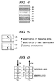
- Fig. 4 illustrates the layer configuration of the magnetoresistance device of the present invention.
- Fig. 5 illustrates magnetization directions of the respective magnetic layers in the magnetoresistance device of an embodiment of the present invention.
- Fig. 6 illustrates recording magnetic fields and magnetization directions at the time of recording in the magnetoresistance device of an embodiment of the present invention.
- Fig. 7 illustrates detecting magnetic fields and magnetization directions at the time of detection in the magnetoresistance device of an embodiment of the present invention.
- Fig. 8 illustrates a time chart showing a detecting magnetic field and changes in resistance differences.
- FIG. 4 An example of the layer configuration of the magnetoresistance device of an embodiment of the present invention is shown in Fig. 4. It has a layer configuration that a first magnetic layer 21, a second magnetic layer 22, a non-magnetic layer 23, a third magnetic layer 24, a fourth magnetic layer 25 and a protective layer 26 are superposed in this order on a substrate 10.
- the substrate 10 usable are, e.g., a silicon substrate and a glass substrate.
- first and forth magnetic layers a magnetic material showing a vertical magnetic anisotropy is used.
- the first magnetic layer stands exchange-coupled with the second magnetic layer, and the third magnetic layer with the fourth magnetic layer.
- the second magnetic layer and the third magnetic layer may have either of a magnetic anisotropy in the film in-plane direction and a magnetic anisotropy in the film-plane normal direction.
- their magnetization directions are parallel to the magnetization directions of perpendicular-magnetizing films standing exchange-coupled with these layers, and these layer are in a state hardly magnetizable in the film in-plane direction.
- keeping perpendicular the magnetization directions of the second magnetic layer and the third magnetic layer depends on the first magnetic layer and the fourth magnetic layer. This enables wide-range selection of materials usable in the second magnetic layer and the third magnetic layer.
- the magnitude of coercivity of the second magnetic layer when it stands exchange-coupled with the first magnetic layer must be different from the magnitude of coercivity of the third magnetic layer when it stands exchange-coupled with the fourth magnetic layer.
- a material which is less oxidizable than rare-earth metals and has a high magnetoresistance ratio (spin polarization ratio).
- a magnetic-layer material may include Fe, CoCr 20 , Co, CoFe, Ni and NiFe.
- the non-magnetic layer it may be formed of either of, e.g., a conductor such as Cu and an insulator such as aluminum oxide.
- the protective layer may preferably be formed of a material containing no oxygen atom, including, e.g., platinum and SiN.
- the layer configuration as described above makes it possible to obtain a magnetoresistance device very small in size that is operable at a small applied magnetic field and has a relatively high magnetoresistance ratio.
- the magnetoresistance ratio increases with a decrease in thickness of the non-magnetic layer in the case of spin-scattering type magnetoresistance devices.
- the magnetostatic coupling force of the magnetic layers provided above and below a non-magnetic layer becomes stronger with a decrease in thickness of the non-magnetic layer, and any antiparallel state of magnetization can not be obtained, resulting in a decrease in the magnetoresistance ratio on the contrary.
- the magnetization of magnetic atoms at the interface between the second magnetic layer and the non-magnetic layer or between the third magnetic layer and the non-magnetic layer and in the vicinity thereof may deviate from the desired direction, resulting in a low magnetoresistance ratio.
- the magnetization of the magnetic layers provided above and below the non-magnetic layer may be made small. Accordingly, in the magnetoresistance device of the present invention, the combined magnetization of the first magnetic layer and the magnetization of the second magnetic layer may preferably be in magnitudes substantially equal to each other and be in directions antiparallel to each other. Also the magnetization of the third magnetic layer and the combined magnetization of the fourth magnetic layer may preferably be in magnitudes substantially equal to each other and be in directions antiparallel to each other.
- any recording in the respective magnetic layers can not be performed.
- transition metals are used in the second magnetic layer and the third magnetic layer
- rare-earth secondary-lattice predominantly magnetizable ferrimagnetic alloys comprised of a rare-earth metal and a transition metal are used in the first magnetic layer and the fourth magnetic layer. Since the first magnetic layer stands exchange-coupled with the second magnetic layer and the third magnetic layer with the fourth magnetic layer, as shown in Fig. 5 the magnetization of the transition metal in the first magnetic layer is parallel to the magnetization of the transition metal in the second magnetic layer, and the magnetization of the rare-earth metal in the first magnetic layer is antiparallel to the magnetization of the transition metal in the second magnetic layer. The like relationship is established also in the third magnetic layer and the fourth magnetic layer.
- compositions of the first magnetic layer and the fourth magnetic layer or the layer thickness of the respective magnetic layers may be adjusted so that the magnitude of total magnetization of transition metals in the first magnetic layer and second magnetic layer (likewise in the third magnetic layer and fourth magnetic layer) may be made substantially equal to the magnitude of magnetization of rare-earth metals in those layers, thus the apparent magnitude of magnetization of the respective exchange-coupled films can be made small.
- the magnetostatic coupling force acting on the magnetic layers provided above and below the non-magnetic layer can be made small.
- An exchange-coupled film of the first magnetic layer and second magnetic layer is set as a memory layer (a layer in which information is accumulated in accordance with the magnetization directions) and an exchange-coupled film of the third magnetic layer and fourth magnetic layer is set as a detecting layer.
- the memory layer has a coercivity larger than that of the detecting layer.
- recording is performed by applying a recording magnetic field Hw.
- the case where the magnetization direction of the memory layer is downward is regarded as "O", and the case where it is upward as “1".
- the composition of the first magnetic layer and fourth magnetic layer may preferably be transition metal secondary-lattice predominantly magnetizable. Detection is performed by changing the magnetization directions of the detecting layer, utilizing the effect of magnetoresistance.
- the magnetoresistance is different between the case where the magnetization in the magnetic layers provided above and below the non-magnetic layer is parallel and the case where it is antiparallel.
- the magnetoresistance is larger in the case where the magnetization is antiparallel than in the case where it is parallel.
- the magnetoresistance is detected by detecting changes in voltage when a constant electric current is flowed through the device and the magnetization direction of the detecting layer reverses under application of a magnetic field at a constant intensity.
- the electric current is flowed in the film-plane normal (vertical) direction in the case of the spin tunnel type.
- the magnetization of the detecting layer is reversed by applying a detecting magnetic field Ha as shown in Fig. 7.
- the magnitude of Ha is so determined that when Ha is applied the magnetization direction of the memory layer does not reverse and the magnetization direction of the detecting layer reverses.
- Fig. 8 is a time chart showing the relationship between the detecting magnetic field Ha and magnetoresistance R. As shown in Fig. 7, Ha is first applied upward and then applied downward. Here, the magnetization direction where "0" has been recorded is regarded as the downward direction. It is seen that when “0” is recorded the magnetoresistance decreases before and after the Ha reverses, and when "1" is recorded the magnetoresistance increases on the contrary. In accordance with changes of this magnetoresistance device, recorded information can be detected non-destructively.
- the inside of a chamber was evacuated to 1 ⁇ 10 -5 Pa or less. Thereafter, on a glass substrate, films were formed by magnetron DC sputtering, as described in the following Examples and Comparative Examples.
- Ar gas pressure was kept constant at 0.3 Pa.
- the magnetic layers were formed at 300 W, and the Cu and Pt layers at 150 W.
- a rare-earth metal secondary-lattice predominantly magnetizable Gd 25 Fe 75 film 20 nm thick as the first magnetic layer, an Fe film 1 nm thick as the second magnetic layer and an Al film 1.6 nm thick as the non-magnetic layer were laminated. Then, O 2 gas was introduced into the chamber so as to provide a pressure of 1 kPa, which was maintained for 1 hour to oxidize the Al layer.
- the inside of the chamber was again evacuated to 1 ⁇ 10 -5 Pa or less, and an Fe film 1 nm thick as the third magnetic layer, a rare-earth metal secondary-lattice predominantly magnetizable Gd 26 Fe 74 film 20 nm thick as the fourth magnetic layer and a Pt film 3 nm thick as the protective layer were formed in this order.
- the magnetic layers and the protective layer were formed under the same sputtering pressure and film formation powers as in Example 1.
- a transition metal secondary-lattice predominantly magnetizable Gd 22 Fe 78 film 10 nm thick as the memory layer, a Cu film 6 nm thick as the non-magnetic layer, a transition metal secondary-lattice predominantly magnetizable Gd 20 Fe 80 film 10 nm thick as the detecting layer and a Pt film 3 nm thick as the protective layer were formed in this order under the same sputtering pressure and film formation powers as in Example 1.
- a CoCr 20 alloy film 2.5 nm thick as the memory layer, a Cu film 3.5 nm thick as the non-magnetic layer, a CoCr 20 alloy film 1.5 nm thick as the detecting layer and a Pt film 3 nm thick as the protective layer were formed in this order under the same sputtering pressure (0.3 Pa) and film formation powers as in Example 1.
- magnetoresistance device To the magnetoresistance device thus obtained, a magnetic field was applied in its film-plane vertical direction, and the magnetization curve was measured to find that any stepwise magnetization curve was obtainable. Also, magnetization-saturating magnetic field was in a value as large as 9.3 kOe.
- a rare-earth metal secondary-lattice predominantly magnetizable Gd 25 Fe 75 film 10 nm thick as the memory layer and an Al film 1.6 nm thick as the non-magnetic layer were laminated. Then, O 2 gas was introduced into the chamber so as to provide a pressure of 1 kPa, which was maintained for 1 hour to oxidize the Al layer. Thereafter, the inside of the chamber was again evacuated to 1 ⁇ 10 -5 Pa or less, and a rare-earth metal secondary-lattice predominantly magnetizable Gd 26 Fe 74 film 10 nm thick as the detecting layer and a Pt film 3 nm thick as the protective layer were formed in this order. The magnetic layers and the protective layer were formed under the same conditions as in Example 1.
- Examples 1 to 4 the devices are seen to have a sufficient magnetoresistance ratio. These magnetoresistance devices shown in Examples have the magnetic anisotropy in the film-plane normal direction. Hence, even with achievement of scale-down, there can be no increase in inverse magnetic fields and also no unstable magnetization.
- the magnetoresistance device of an embodiment of the present invention has the following effects.
- the magnetization directions of the magnetic layers exchange-coupled with each other are set antiparallel, the magnetostatic coupling force can be made small.
- the magnetization directions of the second magnetic layer and third magnetic layer can readily be made to stand antiparallel, and a much higher magnetoresistance ratio can be materialized.
- the magnetic layers do not deteriorate even when oxygen is contained in the non-magnetic layer, and a relatively high magnetoresistance ratio can be obtained.
Landscapes
- Engineering & Computer Science (AREA)
- Chemical & Material Sciences (AREA)
- Nanotechnology (AREA)
- Crystallography & Structural Chemistry (AREA)
- Physics & Mathematics (AREA)
- Mathematical Physics (AREA)
- Theoretical Computer Science (AREA)
- Power Engineering (AREA)
- Computer Hardware Design (AREA)
- Hall/Mr Elements (AREA)
- Semiconductor Memories (AREA)
Abstract
Description
| Measured sample | Magnetoresistance ratio |
| Example 1 | 4.6 |
| Example 2 | 6.7 |
| Example 3 | 14.2 |
| Example 4 | 8.3 |
| Comparative Example 1 | 1.0 |
| Comparative Example 2 | no change |
| Comparative Example 3 | no change |
Claims (11)
- A magnetoresistance device comprising;a multi-layer film having a first magnetic layer, a second magnetic layer, a non-magnetic layer, a third magnetic layer and a fourth magnetic layer which are superposed in this order;wherein the first magnetic layer stands exchange-coupled with the second magnetic layer, and the third magnetic layer exchange-coupled with the fourth magnetic layer, and both the first magnetic layer and the fourth magnetic layer have a magnetic anisotropy in the film-plane normal direction.
- The magnetoresistance device according to claim 1, wherein the second magnetic layer and the third magnetic layer have a higher spin polarization ratio than the first magnetic layer and the fourth magnetic layer.
- The magnetoresistance device according to claim 2, wherein the first magnetic layer and the fourth magnetic layer each comprise an alloy of a rare-earth metal and a transition metal.
- The magnetoresistance device according to claim 2, wherein the second magnetic layer and the third magnetic layer each comprise a transition metal.
- The magnetoresistance device according to claim 1, wherein the magnetization of the first magnetic layer and second magnetic layer and the magnetization of the third magnetic layer and fourth magnetic layer are antiparallel to each other.
- The magnetoresistance device according to claim 5, wherein the magnetization of the first magnetic layer and second magnetic layer and the magnetization of the third magnetic layer and fourth magnetic layer reverse simultaneously in their respective desired applied magnetic fields.
- The magnetoresistance device according to claim 1, wherein the non-magnetic layer comprises a conductor.
- The magnetoresistance device according to claim 1, wherein the non-magnetic layer comprises an insulator.
- A recording device comprising a magnetoresistive device according to any one of claims 1 to 8.
- A method of recording information on a recording device according to claim 9.
- A method of reproducing information recorded on a recording device according to claim 9.
Applications Claiming Priority (2)
| Application Number | Priority Date | Filing Date | Title |
|---|---|---|---|
| JP10957199 | 1999-04-16 | ||
| JP10957199A JP3559722B2 (en) | 1999-04-16 | 1999-04-16 | Magnetoresistive element, solid-state memory |
Publications (3)
| Publication Number | Publication Date |
|---|---|
| EP1045403A2 true EP1045403A2 (en) | 2000-10-18 |
| EP1045403A3 EP1045403A3 (en) | 2001-03-21 |
| EP1045403B1 EP1045403B1 (en) | 2008-07-09 |
Family
ID=14513633
Family Applications (1)
| Application Number | Title | Priority Date | Filing Date |
|---|---|---|---|
| EP00303165A Expired - Lifetime EP1045403B1 (en) | 1999-04-16 | 2000-04-14 | Magnetoresistance device |
Country Status (4)
| Country | Link |
|---|---|
| US (1) | US6721137B1 (en) |
| EP (1) | EP1045403B1 (en) |
| JP (1) | JP3559722B2 (en) |
| DE (1) | DE60039385D1 (en) |
Cited By (3)
| Publication number | Priority date | Publication date | Assignee | Title |
|---|---|---|---|---|
| EP1244117A3 (en) * | 2001-03-19 | 2003-07-16 | Canon Kabushiki Kaisha | Magnetoresistive element, memory element using the magnetorestistive element, and recording/reproduction method for the memory element |
| US6791866B2 (en) | 2001-10-01 | 2004-09-14 | Canon Kabushiki Kaisha | Magnetoresistive film, method of manufacturing magnetoresistive film, and memory using magnetoresistive film |
| WO2004075197A3 (en) * | 2003-01-14 | 2005-03-03 | Infineon Technologies Ag | Mram memory cell |
Families Citing this family (8)
| Publication number | Priority date | Publication date | Assignee | Title |
|---|---|---|---|---|
| JP4944315B2 (en) * | 2001-08-13 | 2012-05-30 | キヤノン株式会社 | Magnetoresistive film, memory element including the same, and memory using the same |
| US6667897B1 (en) * | 2002-06-28 | 2003-12-23 | International Business Machines Corporation | Magnetic tunnel junction containing a ferrimagnetic layer and anti-parallel layer |
| US7602591B2 (en) * | 2005-06-22 | 2009-10-13 | Tdk Corporation | Exchange-coupled free layer with out-of-plane magnetization |
| JP4380707B2 (en) | 2007-01-19 | 2009-12-09 | ソニー株式会社 | Memory element |
| US7929258B2 (en) * | 2008-01-22 | 2011-04-19 | Seagate Technology Llc | Magnetic sensor including a free layer having perpendicular to the plane anisotropy |
| US20090257168A1 (en) * | 2008-04-11 | 2009-10-15 | Northern Lights Semiconductor Corp. | Apparatus for Storing Electrical Energy |
| US20100214718A1 (en) * | 2009-02-24 | 2010-08-26 | Chia-Fu Yeh | Magnetic capacitor |
| US11804322B1 (en) | 2023-07-03 | 2023-10-31 | King Faisal University | Ultra-density nanostructure GdFe thin film with large perpendicular magnetic anisotropy for a new generation of spintronic device |
Family Cites Families (7)
| Publication number | Priority date | Publication date | Assignee | Title |
|---|---|---|---|---|
| US4103315A (en) * | 1977-06-24 | 1978-07-25 | International Business Machines Corporation | Antiferromagnetic-ferromagnetic exchange bias films |
| US5390061A (en) * | 1990-06-08 | 1995-02-14 | Hitachi, Ltd. | Multilayer magnetoresistance effect-type magnetic head |
| JPH08503336A (en) * | 1992-11-16 | 1996-04-09 | ノンボラタイル エレクトロニクス,インコーポレイテッド | Magnetoresistive structure with alloy layer |
| US5652054A (en) * | 1994-07-11 | 1997-07-29 | Kabushiki Kaisha Toshiba | Magnetic recording media having a magnetic thin film made of magnetic metals grains and nonmagnetic matrix |
| US5729410A (en) * | 1996-11-27 | 1998-03-17 | International Business Machines Corporation | Magnetic tunnel junction device with longitudinal biasing |
| JP3679593B2 (en) | 1998-01-28 | 2005-08-03 | キヤノン株式会社 | Magnetic thin film element, magnetic thin film memory element and recording / reproducing method thereof |
| EP0959475A3 (en) * | 1998-05-18 | 2000-11-08 | Canon Kabushiki Kaisha | Magnetic thin film memory and recording and reproducing method and apparatus using such a memory |
-
1999
- 1999-04-16 JP JP10957199A patent/JP3559722B2/en not_active Expired - Fee Related
-
2000
- 2000-04-13 US US09/549,232 patent/US6721137B1/en not_active Expired - Lifetime
- 2000-04-14 DE DE60039385T patent/DE60039385D1/en not_active Expired - Lifetime
- 2000-04-14 EP EP00303165A patent/EP1045403B1/en not_active Expired - Lifetime
Cited By (4)
| Publication number | Priority date | Publication date | Assignee | Title |
|---|---|---|---|---|
| EP1244117A3 (en) * | 2001-03-19 | 2003-07-16 | Canon Kabushiki Kaisha | Magnetoresistive element, memory element using the magnetorestistive element, and recording/reproduction method for the memory element |
| CN100490003C (en) * | 2001-03-19 | 2009-05-20 | 佳能株式会社 | Magnetic resistance element, storage element using same and relative recording/reproducing method |
| US6791866B2 (en) | 2001-10-01 | 2004-09-14 | Canon Kabushiki Kaisha | Magnetoresistive film, method of manufacturing magnetoresistive film, and memory using magnetoresistive film |
| WO2004075197A3 (en) * | 2003-01-14 | 2005-03-03 | Infineon Technologies Ag | Mram memory cell |
Also Published As
| Publication number | Publication date |
|---|---|
| DE60039385D1 (en) | 2008-08-21 |
| US6721137B1 (en) | 2004-04-13 |
| JP2000306374A (en) | 2000-11-02 |
| JP3559722B2 (en) | 2004-09-02 |
| EP1045403B1 (en) | 2008-07-09 |
| EP1045403A3 (en) | 2001-03-21 |
Similar Documents
| Publication | Publication Date | Title |
|---|---|---|
| KR100334837B1 (en) | Spin-valve magnetoresistive thin film element and method of manufacturing the same | |
| US6650513B2 (en) | Magnetic devices with a ferromagnetic layer having perpendicular magnetic anisotropy and an antiferromagnetic layer for perpendicularly exchange biasing the ferromagnetic layer | |
| US6111729A (en) | Magnetoresistance effect element | |
| US7090934B2 (en) | Perpendicular magnetic recording medium | |
| JP3601690B2 (en) | Magnetoresistive element and manufacturing method thereof, magnetoresistive head, magnetic recording device, magnetoresistive memory element | |
| JP3667244B2 (en) | Magnetoresistive element, memory element using the same, magnetic random access memory, and method for recording / reproducing magnetic random access memory | |
| JPH104012A (en) | Magnetoresistive element, method of manufacturing the same, and magnetic head using the same | |
| JPH08503336A (en) | Magnetoresistive structure with alloy layer | |
| JP2003110094A (en) | Magnetic memory using perpendicular magnetization film and method of manufacturing the same | |
| JP2003031867A (en) | Magnetoresistive element with stacked oxide magnetic layer and metal magnetic film | |
| JP3550524B2 (en) | Magnetoresistive element and magnetic memory using the same | |
| JP2817501B2 (en) | Magnetic disk drive and magnetic head used therefor | |
| US6721137B1 (en) | Magnetoresistance device | |
| JP3524486B2 (en) | Magnetoresistance element and memory element using the element | |
| JP3647306B2 (en) | Magnetoresistive element and magnetoresistive memory element | |
| JP4136028B2 (en) | Magnetic thin film memory element, magnetic thin film memory using the same, and recording / reproducing method thereof | |
| JP3544638B2 (en) | Magnetoresistive element and magnetic memory using the same | |
| JP4054403B2 (en) | Magnetic thin film memory | |
| JP2000306376A (en) | Galvanomagnetic effect element and method of reading out its recording | |
| JP2001273757A (en) | Magnetic memory and recording method thereof | |
| JP2003115621A (en) | Tunnel magnetoresistive element and method of manufacturing the same | |
| JP2002324929A (en) | Tunnel magnetoresistive element | |
| JP3204871B2 (en) | Magnetoresistive head | |
| JP2002261351A (en) | Spin valve type thin-film magnetic device and thin-film magnetic head using the same | |
| JP2000306375A (en) | Magnetic resistance element and magnetic memory element |
Legal Events
| Date | Code | Title | Description |
|---|---|---|---|
| PUAI | Public reference made under article 153(3) epc to a published international application that has entered the european phase |
Free format text: ORIGINAL CODE: 0009012 |
|
| AK | Designated contracting states |
Kind code of ref document: A2 Designated state(s): DE FR GB IT NL |
|
| AX | Request for extension of the european patent |
Free format text: AL;LT;LV;MK;RO;SI |
|
| PUAL | Search report despatched |
Free format text: ORIGINAL CODE: 0009013 |
|
| AK | Designated contracting states |
Kind code of ref document: A3 Designated state(s): AT BE CH CY DE DK ES FI FR GB GR IE IT LI LU MC NL PT SE |
|
| AX | Request for extension of the european patent |
Free format text: AL;LT;LV;MK;RO;SI |
|
| RIC1 | Information provided on ipc code assigned before grant |
Free format text: 7H 01F 10/32 A, 7H 01L 43/08 B, 7G 11B 5/39 B, 7G 11C 11/16 B, 7G 11B 5/66 B |
|
| 17P | Request for examination filed |
Effective date: 20010806 |
|
| AKX | Designation fees paid |
Free format text: DE FR GB IT NL |
|
| 17Q | First examination report despatched |
Effective date: 20040217 |
|
| GRAP | Despatch of communication of intention to grant a patent |
Free format text: ORIGINAL CODE: EPIDOSNIGR1 |
|
| GRAS | Grant fee paid |
Free format text: ORIGINAL CODE: EPIDOSNIGR3 |
|
| GRAA | (expected) grant |
Free format text: ORIGINAL CODE: 0009210 |
|
| AK | Designated contracting states |
Kind code of ref document: B1 Designated state(s): DE FR GB IT NL |
|
| REG | Reference to a national code |
Ref country code: GB Ref legal event code: FG4D |
|
| REF | Corresponds to: |
Ref document number: 60039385 Country of ref document: DE Date of ref document: 20080821 Kind code of ref document: P |
|
| PLBE | No opposition filed within time limit |
Free format text: ORIGINAL CODE: 0009261 |
|
| STAA | Information on the status of an ep patent application or granted ep patent |
Free format text: STATUS: NO OPPOSITION FILED WITHIN TIME LIMIT |
|
| 26N | No opposition filed |
Effective date: 20090414 |
|
| PGFP | Annual fee paid to national office [announced via postgrant information from national office to epo] |
Ref country code: FR Payment date: 20110607 Year of fee payment: 12 |
|
| PGFP | Annual fee paid to national office [announced via postgrant information from national office to epo] |
Ref country code: NL Payment date: 20110429 Year of fee payment: 12 |
|
| PGFP | Annual fee paid to national office [announced via postgrant information from national office to epo] |
Ref country code: IT Payment date: 20110412 Year of fee payment: 12 |
|
| REG | Reference to a national code |
Ref country code: NL Ref legal event code: V1 Effective date: 20121101 |
|
| REG | Reference to a national code |
Ref country code: FR Ref legal event code: ST Effective date: 20121228 |
|
| PG25 | Lapsed in a contracting state [announced via postgrant information from national office to epo] |
Ref country code: FR Free format text: LAPSE BECAUSE OF NON-PAYMENT OF DUE FEES Effective date: 20120430 Ref country code: IT Free format text: LAPSE BECAUSE OF NON-PAYMENT OF DUE FEES Effective date: 20120414 |
|
| PG25 | Lapsed in a contracting state [announced via postgrant information from national office to epo] |
Ref country code: NL Free format text: LAPSE BECAUSE OF NON-PAYMENT OF DUE FEES Effective date: 20121101 |
|
| PGFP | Annual fee paid to national office [announced via postgrant information from national office to epo] |
Ref country code: GB Payment date: 20170705 Year of fee payment: 11 |
|
| GBPC | Gb: european patent ceased through non-payment of renewal fee |
Effective date: 20180414 |
|
| PG25 | Lapsed in a contracting state [announced via postgrant information from national office to epo] |
Ref country code: GB Free format text: LAPSE BECAUSE OF NON-PAYMENT OF DUE FEES Effective date: 20180414 |
|
| PGFP | Annual fee paid to national office [announced via postgrant information from national office to epo] |
Ref country code: DE Payment date: 20190621 Year of fee payment: 20 |
|
| REG | Reference to a national code |
Ref country code: DE Ref legal event code: R071 Ref document number: 60039385 Country of ref document: DE |