EP1045273A2 - Reflection type liquid crystal display device with superior display quality - Google Patents
Reflection type liquid crystal display device with superior display quality Download PDFInfo
- Publication number
- EP1045273A2 EP1045273A2 EP00302481A EP00302481A EP1045273A2 EP 1045273 A2 EP1045273 A2 EP 1045273A2 EP 00302481 A EP00302481 A EP 00302481A EP 00302481 A EP00302481 A EP 00302481A EP 1045273 A2 EP1045273 A2 EP 1045273A2
- Authority
- EP
- European Patent Office
- Prior art keywords
- liquid crystal
- recesses
- substrates
- reflection
- reflection member
- Prior art date
- Legal status (The legal status is an assumption and is not a legal conclusion. Google has not performed a legal analysis and makes no representation as to the accuracy of the status listed.)
- Granted
Links
Images





Classifications
-
- G—PHYSICS
- G02—OPTICS
- G02F—OPTICAL DEVICES OR ARRANGEMENTS FOR THE CONTROL OF LIGHT BY MODIFICATION OF THE OPTICAL PROPERTIES OF THE MEDIA OF THE ELEMENTS INVOLVED THEREIN; NON-LINEAR OPTICS; FREQUENCY-CHANGING OF LIGHT; OPTICAL LOGIC ELEMENTS; OPTICAL ANALOGUE/DIGITAL CONVERTERS
- G02F1/00—Devices or arrangements for the control of the intensity, colour, phase, polarisation or direction of light arriving from an independent light source, e.g. switching, gating or modulating; Non-linear optics
- G02F1/01—Devices or arrangements for the control of the intensity, colour, phase, polarisation or direction of light arriving from an independent light source, e.g. switching, gating or modulating; Non-linear optics for the control of the intensity, phase, polarisation or colour
- G02F1/13—Devices or arrangements for the control of the intensity, colour, phase, polarisation or direction of light arriving from an independent light source, e.g. switching, gating or modulating; Non-linear optics for the control of the intensity, phase, polarisation or colour based on liquid crystals, e.g. single liquid crystal display cells
- G02F1/133—Constructional arrangements; Operation of liquid crystal cells; Circuit arrangements
- G02F1/1333—Constructional arrangements; Manufacturing methods
- G02F1/1335—Structural association of cells with optical devices, e.g. polarisers or reflectors
- G02F1/133553—Reflecting elements
-
- G—PHYSICS
- G02—OPTICS
- G02F—OPTICAL DEVICES OR ARRANGEMENTS FOR THE CONTROL OF LIGHT BY MODIFICATION OF THE OPTICAL PROPERTIES OF THE MEDIA OF THE ELEMENTS INVOLVED THEREIN; NON-LINEAR OPTICS; FREQUENCY-CHANGING OF LIGHT; OPTICAL LOGIC ELEMENTS; OPTICAL ANALOGUE/DIGITAL CONVERTERS
- G02F1/00—Devices or arrangements for the control of the intensity, colour, phase, polarisation or direction of light arriving from an independent light source, e.g. switching, gating or modulating; Non-linear optics
- G02F1/01—Devices or arrangements for the control of the intensity, colour, phase, polarisation or direction of light arriving from an independent light source, e.g. switching, gating or modulating; Non-linear optics for the control of the intensity, phase, polarisation or colour
- G02F1/13—Devices or arrangements for the control of the intensity, colour, phase, polarisation or direction of light arriving from an independent light source, e.g. switching, gating or modulating; Non-linear optics for the control of the intensity, phase, polarisation or colour based on liquid crystals, e.g. single liquid crystal display cells
- G02F1/133—Constructional arrangements; Operation of liquid crystal cells; Circuit arrangements
- G02F1/1333—Constructional arrangements; Manufacturing methods
- G02F1/1343—Electrodes
- G02F1/13439—Electrodes characterised by their electrical, optical, physical properties; materials therefor; method of making
-
- G—PHYSICS
- G02—OPTICS
- G02F—OPTICAL DEVICES OR ARRANGEMENTS FOR THE CONTROL OF LIGHT BY MODIFICATION OF THE OPTICAL PROPERTIES OF THE MEDIA OF THE ELEMENTS INVOLVED THEREIN; NON-LINEAR OPTICS; FREQUENCY-CHANGING OF LIGHT; OPTICAL LOGIC ELEMENTS; OPTICAL ANALOGUE/DIGITAL CONVERTERS
- G02F1/00—Devices or arrangements for the control of the intensity, colour, phase, polarisation or direction of light arriving from an independent light source, e.g. switching, gating or modulating; Non-linear optics
- G02F1/01—Devices or arrangements for the control of the intensity, colour, phase, polarisation or direction of light arriving from an independent light source, e.g. switching, gating or modulating; Non-linear optics for the control of the intensity, phase, polarisation or colour
- G02F1/13—Devices or arrangements for the control of the intensity, colour, phase, polarisation or direction of light arriving from an independent light source, e.g. switching, gating or modulating; Non-linear optics for the control of the intensity, phase, polarisation or colour based on liquid crystals, e.g. single liquid crystal display cells
- G02F1/133—Constructional arrangements; Operation of liquid crystal cells; Circuit arrangements
- G02F1/136—Liquid crystal cells structurally associated with a semi-conducting layer or substrate, e.g. cells forming part of an integrated circuit
- G02F1/1362—Active matrix addressed cells
- G02F1/1368—Active matrix addressed cells in which the switching element is a three-electrode device
-
- G—PHYSICS
- G02—OPTICS
- G02F—OPTICAL DEVICES OR ARRANGEMENTS FOR THE CONTROL OF LIGHT BY MODIFICATION OF THE OPTICAL PROPERTIES OF THE MEDIA OF THE ELEMENTS INVOLVED THEREIN; NON-LINEAR OPTICS; FREQUENCY-CHANGING OF LIGHT; OPTICAL LOGIC ELEMENTS; OPTICAL ANALOGUE/DIGITAL CONVERTERS
- G02F1/00—Devices or arrangements for the control of the intensity, colour, phase, polarisation or direction of light arriving from an independent light source, e.g. switching, gating or modulating; Non-linear optics
- G02F1/01—Devices or arrangements for the control of the intensity, colour, phase, polarisation or direction of light arriving from an independent light source, e.g. switching, gating or modulating; Non-linear optics for the control of the intensity, phase, polarisation or colour
- G02F1/13—Devices or arrangements for the control of the intensity, colour, phase, polarisation or direction of light arriving from an independent light source, e.g. switching, gating or modulating; Non-linear optics for the control of the intensity, phase, polarisation or colour based on liquid crystals, e.g. single liquid crystal display cells
- G02F1/137—Devices or arrangements for the control of the intensity, colour, phase, polarisation or direction of light arriving from an independent light source, e.g. switching, gating or modulating; Non-linear optics for the control of the intensity, phase, polarisation or colour based on liquid crystals, e.g. single liquid crystal display cells characterised by the electro-optical or magneto-optical effect, e.g. field-induced phase transition, orientation effect, guest-host interaction or dynamic scattering
- G02F1/139—Devices or arrangements for the control of the intensity, colour, phase, polarisation or direction of light arriving from an independent light source, e.g. switching, gating or modulating; Non-linear optics for the control of the intensity, phase, polarisation or colour based on liquid crystals, e.g. single liquid crystal display cells characterised by the electro-optical or magneto-optical effect, e.g. field-induced phase transition, orientation effect, guest-host interaction or dynamic scattering based on orientation effects in which the liquid crystal remains transparent
- G02F1/1396—Devices or arrangements for the control of the intensity, colour, phase, polarisation or direction of light arriving from an independent light source, e.g. switching, gating or modulating; Non-linear optics for the control of the intensity, phase, polarisation or colour based on liquid crystals, e.g. single liquid crystal display cells characterised by the electro-optical or magneto-optical effect, e.g. field-induced phase transition, orientation effect, guest-host interaction or dynamic scattering based on orientation effects in which the liquid crystal remains transparent the liquid crystal being selectively controlled between a twisted state and a non-twisted state, e.g. TN-LC cell
Definitions
- the present invention relates to a liquid crystal display device and, in particular, to a reflection type liquid crystal display device which effects display by using external light.
- liquid crystal display devices are widely used.
- a reflection type liquid crystal display device using no backlight is effective in achieving a reduction in power consumption.
- a conventional reflection type display device comprises a pair of glass substrates 113 and 114, transparent electrode layers 120 and 121 provided on the opposed surfaces of the glass substrates, liquid crystal orientation films 122 and 123 respectively provided on the transparent electrode layers 120 and 121, and a liquid crystal layer 115 provided between the orientation films 122 and 123.
- first and second polarizing plates 117 and 118 are provided on the outside of the glass substrates 113 and 114, and on the outside of the second polarizing plate 118, there is provided a reflection plate 101, with the surface of a reflection film 105 being directed to the second polarizing plate 118.
- the reflection type liquid crystal display device 100 constructed as described above, light impinging upon the first polarizing plate 117 undergoes linear polarization, and is further transmitted through the liquid crystal layer 115 to become elliptically polarized light. And, the light which has become elliptically polarized light is turned into linearly polarized light by the second polarizing plate 118, reflected by the reflection plate 101, again transmitted through the second polarizing plate 118 and the liquid crystal layer 115 before it is emitted from the first polarizing plate 117.
- the reflection plate 101 is endowed with scattering reflection characteristics by, for example, forming a reflection layer consisting of aluminum or the like on the rough surface of a metal film, synthetic paper or the like.
- Such a reflection plate has wide scattering angle characteristics, so that it is difficult to enhance the bright in a particular direction frequently viewed as in the case of the front of the display surface as seen from the observer. As a result, the display is rather dark although the angle of sight is wide.
- the angle of sight should be wide and much brightness should be obtained.
- recesses are sequentially formed on the surface in a mechanical manner. It is a convenient method to form one or a plurality of shapes at one time in a certain place, feed the sequentially in the X-direction in a fixed pitch, feed the machining position in the Y-direction after machining for a predetermined length, and perform surface processing while feeding in the X-direction again.
- a reflection plate having a repeated arrangement is combined with a stripe-shaped electrode for display electrode, when the directions of these repeated structures do not completely coincide but make a slight angle, periodical overlapping occurs between these patterns, and a fringe-like pattern which is oblique with respect to the pattern direction, a so-called moire fringe, is viewed. Further, even in the case in which a reflection type liquid crystal display device of this type is combined with color filters to perform color display, a moire fringe is to be viewed between the repeated structure of the protrusions and recesses of the reflection plate and the repeated alignment structure of the colored pixels of the color filters, which impairs the display quality.
- the present invention has been made with a view toward solving the above problem. It is an object of the present invention to provide a liquid crystal display device in which oblique moire fringe is not easily viewed while using a reflection plate of satisfactory reflection characteristics with repeated recess arrangement and which is superior in display quality.
- a reflection type liquid crystal display device comprising upper and lower substrates, a liquid crystal layer provided between the upper and lower substrates, a plurality of stripe-like transparent electrodes formed on the side of at least one of the opposed surfaces of the upper and lower substrates so as to extend in a predetermined direction, and a reflection member on the opposed surface side or outside of the lower substrate, the reflection member having a large number of recesses arranged in a direction, wherein the direction in which the recesses are arranged is deviated 2.5 to 40 degrees from the direction in which the stripe-like transparent electrodes extend, whereby the moire fringe is not easily viewed and it is possible to improve the display quality of the liquid crystal display device.
- the reflection member has on its surface a large number of recesses the inner surfaces of which constitute part of spherical surfaces and which are formed continuously so as to overlap each other, the depth of the recesses and the pitch of adjacent recesses varying within predetermined ranges, whereby it is possible to obtain a bright reflection plate free from interference of light, thereby making it possible to improve the display quality of the liquid crystal display device.
- a reflection type liquid crystal display device which adopts an STN or TFT system wherein the reflection member is provided on the liquid crystal layer side of the lower substrate and wherein a polarizing plate is provided on the upper substrate.
- a reflection type liquid crystal display device comprising a pair of substrates, a liquid crystal layer placed between the pair of substrates, a plurality of stripe-like transparent electrodes formed in parallel at predetermined intervals on opposed surfaces of the pair of substrates, the opposed stripe-like transparent electrodes being orthogonal to each other, and a reflection member provided on the side of one of the opposed surfaces of the substrates or on the outside, the reflection member having a large number of recesses continuously formed so as to be arranged in two directions orthogonal to each other, the two directions in which the large number of recesses are arranged are deviated by an angle of 2.5 to 40 degrees from the two directions in which the stripe-like transparent electrodes orthogonal to each other extend.
- the moire fringe interval is small, so that moire fringe is not easily viewed, whereby it is possible to improve the display quality of a liquid crystal display device.
- minute protrusions and recesses are formed on the surface of the reflection member, and the protrusions and recesses are repeatedly arranged according to a fixed regulation.
- a reflection member has a large number of recesses continuously formed on the surface whose inner surface constitutes a part of a spherical surface, the depth of the recesses being in the range of 0.1 to 3 ⁇ m, the inclination angle distribution of the recess inner surface being in the range of -35 degrees to +35 degrees, the pitch of adjacent recesses being in the range of 5 ⁇ m to 50 ⁇ m.
- the “recess depth” is the distance from the surface of the reflection member to the bottom of the recess
- the “pitch of the adjacent recesses” is the distance between the centers of the recesses which are circular in plan view.
- the “inclination angle of the recess inner surface” is the angle of the inclined surface with respect to the horizontal surface in the minute range when a minute range of 0.5 ⁇ m width is taken at an arbitrary position on the inner surface of the recess 4. It is assumed that the angle of the reflection inclined surface of each recess with respect to a normal extending from the reflection member surface is positive and that the angle of the opposed inclined surface is negative.
- the inclination angle distribution is set in the range of -35 degrees to +35 degrees and that the recess pitch is arranged random with respect to all directions of the plane. If there should be any regularity in pitch in adjacent recesses, the interference colors of light would appear, coloring the reflection light. If the inclination angle distribution of the recess inner surface is beyond the range of -35 degrees to +35 degrees, the inclination angle of the reflection light is too wide, and the reflection intensity deteriorates, making it impossible to obtain a bright reflection plate (The diffusion angle of the reflection light is over 70 degrees in the air, resulting in a reduction in the reflection intensity peak in the interior of the liquid crystal display device and an increase in total reflection loss.
- the vortex of the protrusion cannot be buried in the flattening film when flattening the recesses in the post process, making it impossible to achieve a desired flatness.
- the pitch of the adjacent recesses is less than 5 ⁇ m, there is a limitation to the preparation of the mould for forming the reflection member, and a configuration which would provide desired reflection characteristics cannot be obtained, interference light, etc. being generated.
- the pitch of the adjacent recesses it is desirable for the pitch of the adjacent recesses to be 5 to 50 ⁇ m.
- pitch of stripe-like transparent electrodes arranged side by side is 50 to 500 ⁇ m. Further, it is desirable for each line width to be 40 to 490 ⁇ m.
- the pitch of the transparent electrodes arranged side by side is less than 50 ⁇ m, there is a limitation to the machining of the transparent electrodes; if it is more than 500 ⁇ m, the pixels become rather large, making it impossible to obtain desired display characteristics and display quality.
- the line width between the electrodes is less than 40 ⁇ m, there is a limitation to the machining of the transparent electrodes; if it is more than 490 ⁇ m, the pixels become large, making it impossible to obtain desired display characteristics and display quality.
- the two orthogonal directions in which a large number of protrusions and recesses are arranged are deviated 2.5 to 40 degrees from the two directions in which the orthogonal stripe-like electrodes extend since, if the deviation is less than 2.5 degrees, moire fringe that can be viewed will be generated and, if it is more than 40 degrees, another moire fringe that can be viewed will be generated.
- a reflection type liquid crystal display device comprising upper and lower substrates, a liquid crystal layer provided between the upper and lower substrates, a plurality of stripe-like transparent electrodes formed on at least one opposed surface side of the upper and lower substrates so as to extend in a predetermined direction, a reflection member provided on the opposed surface side or outside of the lower substrate, and color filters provided on one of the opposed sides of the upper and lower substrates, the reflection member having a large number of recesses arranged in a direction, wherein the direction in which the recesses are arranged is deviated 2.5 to 40 degrees from the direction in which a plurality of colored pixels of the color filters are aligned, whereby the moire fringe is not easily viewed, thereby achieving an improvement in color display quality.
- a reflection type liquid crystal display device wherein the reflection member has a large number of recesses the inner surfaces of which constitute part of spherical surfaces, the depth of the recesses and the pitch of the recesses varying within predetermined ranges, whereby it is possible to obtain a bright reflection plate free from interference of light, making it possible to achieve an improvement in color display quality.
- a reflection type color liquid crystal display device which adopts an STN or TFT system wherein the reflection member is provided on the liquid crystal layer side of the lower substrate and wherein the color filters or overcoat layer is sequentially provided on the reflection member, a polarizing plate being arranged on the upper substrate.
- a reflection type color liquid crystal display device comprising a pair of substrates, a liquid crystal layer placed between the pair of substrates, a plurality of stripe-like transparent electrodes formed in parallel at predetermined intervals on opposed surfaces of the pair of substrates, the opposed stripe-like transparent electrodes being orthogonal to each other, a reflection member provided on the side of one of the opposed surfaces of the substrates or on the outside, and color filters provided on the side of one of the opposed surfaces of the substrates, the reflection member having a large number of recesses continuously formed so as to be arranged in two directions orthogonal to each other, the two directions in which the large number of recesses are arranged are deviated by an angle of 2.5 to 40 degrees from the two directions in which the stripe-like transparent electrodes orthogonal to each other extend, the two directions in which a plurality of colored pixels of the color filters are aligned are identical with the two directions in which the stripe-like electrodes orthogonal to each other extend.
- the moire fringe can be reduced to such a degree that it is hard to view, and the reflection member provides a high reflection efficiency in all directions, so that, compared with the conventional reflection type color liquid crystal display device, it is possible to provide a reflection type color display device which is brighter and which has more satisfactory display quality.
- reflection member and stripe-like electrodes it is possible to use the reflection member and stripe-like electrodes in the above-described reflection type liquid crystal display device.
- the color filters it is desirable to arrange a plurality of colored pixels in parallel in rows at an inter-row pitch of 50 to 500 ⁇ m, and the row width of each colored pixel row is preferably 40 to 490 ⁇ m. If the inter-row pitch of the colored pixel rows arranged in parallel is less than 50 ⁇ m, there is a limitation to the processing of the colored pixel rows; if it is more than 500 ⁇ m, the pixels become rather large, making it impossible to achieve desired display characteristics and display quality.
- each colored pixel row is less than 40 ⁇ m, there is a limitation to the processing of the colored pixel rows; if it is more than 490 ⁇ m, the pixels become rather large, making it impossible to achieve desired display characteristics and display quality.
- Fig. 1 is a sectional view showing an embodiment of the reflection type liquid crystal display device of the present invention.
- This reflection type liquid crystal display device includes a display side glass substrate 13 and a backside lower glass substrate 14 having a thickness of, for example, 0.7 mm. On the inner side of these glass substrates, there are formed a plurality of stripe-like transparent display electrodes 20 and 21. Further, a liquid crystal layer 15 is provided between these electrodes.
- a phase plate 16 consisting of polycarbonate resin or polyacrylate resin or the like is provided on the upper side of the display side glass substrate 13, and further, a first polarizing plate 17 is arranged on the upper side of the phase plate 16. Further, on the lower side of the backside glass substrate 14, there are sequentially provided a second polarizing plate 18, an adhesive member 19 and a plate-like reflection member 1.
- the plurality of upper transparent electrodes 20 extend in the direction passing through the plane of Fig. 1 and are arranged side by side at fixed intervals.
- the reflection member 1 is attached to the lower side of the second polarizing plate 18 such that it is opposed to the surface on which protrusions and recesses are formed, and the space between the reflection member 1 and the second polarizing plate 18 is filled with an adhesive member 19 consisting of a material such as glycerine which does not adversely affect the refractive index of light.
- the reflection member 1 comprises a substrate 2 consisting, for example, of glass.
- a flat resin base 3 (reflection member base) consisting of a photosensitive resin or the like is provided on the substrate 2.
- a large number of recesses 4 the inner surfaces of which constitute part of spherical surfaces, are continuously formed so as to overlap each other.
- a reflection film 5 consisting of a thin film of aluminum, silver or the like is formed by evaporation or printing.
- the depth of the recesses 4, which is at random be in the range of 0.1 to 3 ⁇ m, and that the adjacent recesses 4 be arranged at random at a pitch in the range of 5 to 50 ⁇ m, the inclination angle of the inner surfaces of the recesses 4 being set in the range of -35 degrees to +35 degrees.
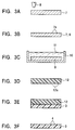
- the reflection member 1 is produced as shown in Figs. 3 through 7.
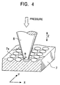
- a mother base material 7 whose surface is flat and which consists, for example, of brass, stainless steel or tool steel, is secured in position on a table of a rolling machine. Then, the surface of the mother base material 7 is depressed by a diamond indenter 8 whose forward end has a spherical configuration with a predetermined diameter R, and the operation of depressing the mother base material while horizontally moving the mother base material 7 is repeated a large number of times, whereby a large number of recesses 7a whose depths and whose arrangement pitches differ are formed by rolling on the surface of the mother base material 7, thereby obtaining a reflection member base 9 as shown in Fig. 3(b).
- the table for securing the mother base material 7 in position moves in the horizontal X and Y-directions with a resolution of 0.1 ⁇ m
- the diamond indenter 8 moves in the vertical direction (Z-direction) with a resolution of 1 ⁇ m.
- the diameter R of the forward end of the diamond indenter 8 be approximately 10 to 100 ⁇ m.
- the diameter R of the forward end of the indenter is 30 to 50 ⁇ m
- the diameter R of the forward end of the indenter is 50 to 100 ⁇ m.
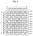
- the rolling by the diamond indenter is conducted by the following procedures.
- the pitches of vertically adjacent recesses from above are similar to the above pattern.
- r1 11 ⁇ m
- r2 10 ⁇ m
- r3 9 ⁇ m
- r4 8 ⁇ m
- the depth radii in a longitudinal row are: r1, r2, r3, r1, r4, r2, r4, r3, r1, r4, r1 from above.
- the mother pattern 9 is accommodated and arranged in a box-like container 10, and a resin material 11 such as silicone is poured into the container 10, the resin material being allowed to stand at room temperature to cure.
- the resin product cured is extracted from the container 10 and the unnecessary portion thereof is cut off, whereby, as shown in Fig. 3(d), a transfer pattern 12 is formed, which includes a pattern surface 12a having a large number of protrusions of a configuration reverse to the large number of recesses constituting the pattern surface of the mother pattern 9.
- a photosensitive resin liquid such as acrylic type resist, polystyrenene type resist, azide rubber type resist, or imide type resist
- a photosensitive resin liquid such as acrylic type resist, polystyrenene type resist, azide rubber type resist, or imide type resist
- pre-baking is conducted, in which the photosensitive resin liquid on the substrate is heated for more than one minute in a temperature range, for example, of 80 to 100°C by using a heating device such as a heating furnace or a hot plate, to thereby form a photosensitive resin layer on the substrate.
- the pre-baking conditions differ according to the kind of photosensitive resin used, so that it is naturally possible to perform the processing at a temperature and for a time beyond the above-mentioned ranges. It is desirable for the thickness of the photosensitive resin layer to be in the range of 2 to 5 ⁇ m.
- the pattern surface 12a of this transfer pattern 12 is pressed against the photosensitive resin layer 3 on the glass substrate for a fixed period of time, and then the transfer pattern 12 is detached from the photosensitive resin layer 3.
- the protrusions of the transfer pattern surface 12a is transferred to the surface of the photosensitive resin layer 3 to form a large number of recesses 4.
- a value is preferably selected which is adapted to the kind of photosensitive resin used; for example, it is a pressure of approximately 30 to 50 kg/cm 2 .
- the press time it is desirable to select a value corresponding to the kind of photosensitive resin used. For example, it is approximately 30 seconds to 10 minutes.
- rays such as ultraviolet rays (g, h, i-rays) for curing the photosensitive resin layer 3 are applied from the back side of the transparent glass substrate to cure the photosensitive resin layer 3.
- an intensity of 50 mJ/cm 2 or more is enough for the rays such as ultraviolet rays applied to cure the photosensitive resin layer.
- post baking is conducted, in which by using a heating device such as a heating furnace or hot plate which is the same as used in the pre-baking, the photosensitive resin layer 3 on the glass substrate 3 is heated for one minute or more at approximately 240°C to bake the photosensitive resin layer 3 on the glass substrate.
- a heating device such as a heating furnace or hot plate which is the same as used in the pre-baking
- a film of aluminum or the like is formed by electron beam evaporation or the like to form a reflection film 5 along the surface of the recess, thereby completing the reflection member 1.
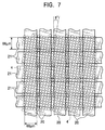
- the transparent electrodes 20 and 21 have a stripe-like pattern, and when the pitch of the adjacent row of recesses in the reflection member 1 is 10 to 20 ⁇ m, they are formed at a vertical pitch of 76 ⁇ m and with a shorter width of 66 ⁇ m.
- the direction in which the rows of recesses 4 of the reflection member 1 are arranged is set beforehand such that it makes an angle of 8 degrees with respect to the direction in which the stripe-like transparent electrodes 20 extend.
- the pitch of the moire fringe generated as a result of the reflection member 1 being superimposed on the transparent electrodes 20 is approximately 1.07 ⁇ m, so that the moire fringe is not easily viewed. Further, if an angle deviation of 0.5 degrees occurs, the change in the pitch of the moire fringe generated as a result of superimposing is approximately 7 ⁇ m, so that the change occurs to a small degree.
- the reflection member 1 may be directly formed on the opposed surface of the lower substrate 14, for example, on the substrate 14.
- the direction in which the stripe-like electrodes 20 extend intersects the rows of recesses 4 of the reflection member 1 at an angle of 8 degrees as shown in Fig. 7.
- FIG. 8 Another embodiment of a reflection type color liquid crystal display device will be described with reference to Fig. 8.
- the basic construction of this embodiment is the same as that of the above-described reflection type liquid crystal display device.
- a resin layer 33 having a large number of protrusions and recesses there are sequentially stacked on the opposed surface of the lower glass substrate 44, a resin layer 33 having a large number of protrusions and recesses, a reflection film 35 consisting of a metal such as aluminum, the resin layer 33 and the reflection film 35 constituting a reflection member 30, a flattening layer 41, a plurality of stripe-like lower transparent electrodes 51 consisting of indium tin oxide (hereinafter referred to as ITO) and an orientation film 53.
- ITO indium tin oxide
- an STN liquid crystal layer 45 is sealed in.
- a first phase plate 46 Outside the upper glass substrate 43, there are sequentially provided a first phase plate 46, a second phase plate 47 and a polarizing plate 48.
- the plurality of lower transparent electrodes 51 extend laterally in Fig. 8 and are arranged side by side at predetermined intervals.
- the plurality of upper transparent electrodes 20 extend in a direction in which they pass through the plane of Fig. 1, and are arranged side by side at predetermined intervals.
- inter-electrode pitch of these upper and lower transparent electrodes 50 and 51 and the shorter side width of each electrode are the same as those of the electrodes 20 and 21 shown in Fig. 1.
- the color filters 60 consist of a plurality of elongated rectangular colored pixels 60a formed in correspondence with the upper transparent electrodes 50.
- the arrangement of the colored pixels 60a of the color filters 60 is such that the colored pixels 60a are arranged alternately longitudinally or laterally in a stripe-like manner in the order of red (R), green (G) and blue (B).
- the shorter side width W1 of each colored pixel 60a is not less than 80% of the shorter side width W2 of the corresponding upper transparent electrode 50, and they are provides so as not to overlap the adjacent colored pixels.
- each colored pixel 60a When the shorter side width of each colored pixel 60a is less than 80% of the shorter side width of the corresponding upper transparent electrode 50, a reduction in chromaticity occurs, and the color display quality deteriorates, and when it overlaps the adjacent colored pixel, a step is generated where they overlap each other, resulting in a deterioration in display quality due to orientation unevenness.
- the reflection member 30 is of the same construction as the reflection member 1 shown in Fig. 2 excluding the substrate 2. That is, the resin layer 33 corresponds to the resin layer 3 in Fig. 2, and the reflection film 35 corresponds to the reflection film 5 in Fig. 2. Thus, as shown in Fig. 9, the large number of recesses 34 in this reflection member 30 are of the same construction as the recesses 4 shown in Figs. 2 and 6.
- the recesses 34 of the reflection member 30 are arranged beforehand in a direction which makes an angle of 8 degrees with respect to the direction in which the stripe-like transparent electrodes 50 extend.
- the rows of recesses 34 of the reflection member 30 are arranged beforehand in a direction which makes an angle of 8 degrees with respect to the direction in which the colored pixels 60a of the color filters are arranged.
- the pitch of the moire fringe generated as a result of superimposing of the reflection member 30, the transparent electrodes 50 and the colored pixels 60a is approximately 107 ⁇ m, so that the moire fringe is not easily viewed.
- the reflection member 30 may be provided on the outer side of the lower substrate 44 instead of providing it on the inner side thereof. Further, instead of providing the providing the color filters 60 on the upper substrate 43 side, it is possible to provide them on the lower substrate 44 side. For example, it is possible to adopt a construction in which the color filters 60 and the overcoat layer 42 are sequentially provided on the reflection member 30 and in which the flattening layer 41 is omitted. Further, it goes without saying that the reflection member of the present invention is applicable not only to an STN (super twisted nematic) type but also to a TN (twisted nematic) type liquid crystal display device, for example, a TFT type liquid crystal display device.
- the direction in which the stripe-like display electrodes extend is deviated 2.5 to 40 degrees from the direction in which a large number of recesses of the reflection member are repeatedly arranged, whereby the moire fringe is not conspicuous, and it is possible to obtain a bright display with high display quality.
- the depth of the recesses and the pitch of the adjacent recesses of the reflection plate vary within predetermined ranges, there is no interference of light, and the reflection efficiency is enhanced in all directions, whereby it is possible to obtain a bright display quality.
- the direction in which the colored pixels of the color filters are arranged is deviated 2.5 to 40 degrees from the direction in which a large number recesses of the reflection member are repeatedly arranged, whereby the moire fringe is not conspicuous, and it is possible to obtain a bright display with high display quality.
- the depth of the recesses and the pitch of the adjacent recesses of the reflection plate vary within predetermined ranges, there is no interference of light, and the reflection efficiency is enhanced in all directions, whereby it is possible to obtain a bright display quality.
Landscapes
- Physics & Mathematics (AREA)
- Nonlinear Science (AREA)
- Chemical & Material Sciences (AREA)
- Crystallography & Structural Chemistry (AREA)
- General Physics & Mathematics (AREA)
- Optics & Photonics (AREA)
- Mathematical Physics (AREA)
- Engineering & Computer Science (AREA)
- Microelectronics & Electronic Packaging (AREA)
- Liquid Crystal (AREA)
- Optical Elements Other Than Lenses (AREA)
Abstract
Description
Claims (8)
- A reflection type liquid crystal display device comprising upper and lower substrates, a liquid crystal layer provided between the upper and lower substrates, a plurality of stripe-like transparent electrodes formed on the side of at least one of the opposed surfaces of the upper and lower substrates so as to extend in a predetermined direction, and a reflection member on the opposed surface side or outside of the lower substrate, the reflection member having a large number of recesses arranged in a direction, wherein the direction in which the recesses are arranged is deviated 2.5 to 40 degrees from the direction in which the stripe-like transparent electrodes extend.
- A reflection type liquid crystal display device according to Claim 1, wherein the reflection member has on its surface a large number of recesses the inner surfaces of which constitute part of spherical surfaces and which are formed continuously so as to overlap each other, the depth of the recesses and the pitch of adjacent recesses varying within predetermined ranges.
- A reflection type liquid crystal display device according to Claim 1 or 2, wherein an STN or TFT system is adoptetd wherein the reflection member is provided on the liquid crystal layer side of the lower substrate and wherein a polarizing plate is provided on the upper substrate.
- A reflection type liquid crystal display device comprising upper and lower substrates, a liquid crystal layer provided between the upper and lower substrates, a plurality of stripe-like transparent electrodes formed on at least one opposed surface side of the upper and lower substrates so as to extend in a predetermined direction, a reflection member provided on the opposed surface side or outside of the lower substrate, and color filters provided on one of the opposed sides of the upper and lower substrates, the reflection member having a large number of recesses arranged in a direction, wherein the direction in which the recesses are arranged is deviated 2.5 to 40 degrees from the direction in which a plurality of colored pixels of the color filters are aligned.
- A reflection type liquid crystal display device according to Claim 4, wherein the reflection member has a large number of recesses the inner surfaces of which constitute part of spherical surfaces, the depth of the recesses and the pitch of the adjacent recesses varying within predetermined ranges.
- A reflection type liquid crystal display device according to Claim 4 or 5, wherein an STN or TFT system is adopted wherein the reflection member is provided on the liquid crystal layer side of the lower substrate and wherein the color filters or overcoat layer is sequentially provided on the reflection member, a polarizing plate being arranged on the upper substrate.
- A reflection type liquid crystal display device comprising a pair of substrates, a liquid crystal layer placed between the pair of substrates, a plurality of stripe-like transparent electrodes formed in parallel at predetermined intervals on opposed surfaces of the pair of substrates, the opposed stripe-like transparent electrodes being orthogonal to each other, and a reflection member provided on the side of one of the opposed surfaces of the substrates or on the outside, the reflection member having a large number of recesses continuously formed so as to be arranged in two directions orthogonal to each other, the two directions in which the large number of recesses are arranged are deviated by an angle of 2.5 to 40 degrees from the two directions in which the stripe-like transparent electrodes orthogonal to each other extend.
- A reflection type liquid crystal display device comprising a pair of substrates, a liquid crystal layer placed between the pair of substrates, a plurality of stripe-like transparent electrodes formed in parallel at predetermined intervals on opposed surfaces of the pair of substrates, the opposed stripe-like transparent electrodes being orthogonal to each other, a reflection member provided on the side of one of the opposed surfaces of the substrates or on the outside, and color filters provided on the side of one of the opposed surfaces of the substrates, the reflection member having a large number of recesses continuously formed so as to be arranged in two directions orthogonal to each other, the two directions in which the large number of recesses are arranged are deviated by an angle of 2.5 to 40 degrees from the two directions in which the stripe-like transparent electrodes orthogonal to each other extend, the two directions in which a plurality of colored pixels of the color filters are aligned are identical with the two directions in which the stripe-like electrodes orthogonal to each other extend.
Applications Claiming Priority (2)
| Application Number | Priority Date | Filing Date | Title |
|---|---|---|---|
| JP11105868A JP2000298274A (en) | 1999-04-13 | 1999-04-13 | Reflection-type liquid crystal display device |
| JP10586899 | 1999-04-13 |
Publications (3)
| Publication Number | Publication Date |
|---|---|
| EP1045273A2 true EP1045273A2 (en) | 2000-10-18 |
| EP1045273A3 EP1045273A3 (en) | 2004-04-28 |
| EP1045273B1 EP1045273B1 (en) | 2006-07-05 |
Family
ID=14418946
Family Applications (1)
| Application Number | Title | Priority Date | Filing Date |
|---|---|---|---|
| EP00302481A Expired - Lifetime EP1045273B1 (en) | 1999-04-13 | 2000-03-27 | Reflection type liquid crystal display device with superior display quality |
Country Status (7)
| Country | Link |
|---|---|
| US (1) | US6686982B1 (en) |
| EP (1) | EP1045273B1 (en) |
| JP (1) | JP2000298274A (en) |
| KR (1) | KR100367897B1 (en) |
| CN (1) | CN1125366C (en) |
| DE (1) | DE60029161T2 (en) |
| TW (1) | TW496983B (en) |
Cited By (2)
| Publication number | Priority date | Publication date | Assignee | Title |
|---|---|---|---|---|
| EP1279994A3 (en) * | 2001-07-27 | 2003-10-01 | Alps Electric Co., Ltd. | Semitransparent reflective liquid-crystal display device |
| KR100576273B1 (en) * | 2001-07-27 | 2006-05-04 | 알프스 덴키 가부시키가이샤 | Liquid crystal display |
Families Citing this family (10)
| Publication number | Priority date | Publication date | Assignee | Title |
|---|---|---|---|---|
| WO2001079896A1 (en) * | 2000-04-17 | 2001-10-25 | Matsushita Electric Industrial Co., Ltd. | REFLECTION BOARd, REFLECTION TYPE LIQUID CRYSTAL DISPLAY UNIT AND PRODUCTION METHOD THEREFOR, OPTICAL MEMBER, DISPLAY UNIT, ILLUMINATING DEVICE, DISPLAY BOARD, AND UNDULATORY MEMBER |
| JP2003150073A (en) * | 2001-08-27 | 2003-05-21 | Omron Corp | Image display device and front light |
| KR100617029B1 (en) * | 2001-12-29 | 2006-08-30 | 엘지.필립스 엘시디 주식회사 | Manufacturing method of liquid crystal display device |
| TWI227806B (en) * | 2002-05-30 | 2005-02-11 | Fujitsu Display Tech | Substrate for liquid crystal display, liquid crystal display having the same, and method of manufacturing the same |
| JP3742038B2 (en) * | 2002-08-01 | 2006-02-01 | Nec液晶テクノロジー株式会社 | Liquid crystal display device and manufacturing method thereof |
| JP3800186B2 (en) | 2003-02-21 | 2006-07-26 | セイコーエプソン株式会社 | Liquid crystal display device, reflector, and electronic device |
| KR101064189B1 (en) * | 2004-08-03 | 2011-09-14 | 삼성전자주식회사 | Color filter substrate, display panel and manufacturing method thereof |
| US20090279018A1 (en) * | 2008-05-08 | 2009-11-12 | Ching-Bin Lin | Optical device having light diffusing paper incorporated therewith |
| KR101628465B1 (en) * | 2014-07-17 | 2016-06-09 | 하이디스 테크놀로지 주식회사 | Flat Panel Display Device with Overcoat Layer for reducing Moire and Method For Forming the Device |
| KR102555999B1 (en) * | 2018-07-23 | 2023-07-14 | 삼성디스플레이 주식회사 | Display device |
Family Cites Families (10)
| Publication number | Priority date | Publication date | Assignee | Title |
|---|---|---|---|---|
| JPS5435780B2 (en) * | 1974-07-23 | 1979-11-05 | ||
| CH633381A5 (en) * | 1978-12-20 | 1982-11-30 | Bbc Brown Boveri & Cie | ELECTROOPTICAL DISPLAY WITH REFLECTOR. |
| JPH0868997A (en) * | 1994-08-30 | 1996-03-12 | Hitachi Ltd | Liquid crystal display |
| JP3075134B2 (en) | 1995-04-04 | 2000-08-07 | 株式会社日立製作所 | Reflective liquid crystal display |
| US5919551A (en) * | 1996-04-12 | 1999-07-06 | 3M Innovative Properties Company | Variable pitch structured optical film |
| JPH10232395A (en) * | 1996-12-18 | 1998-09-02 | Sumitomo Chem Co Ltd | Reflective liquid crystal display |
| JP3621226B2 (en) * | 1997-05-12 | 2005-02-16 | アルプス電気株式会社 | REFLECTOR, MANUFACTURING METHOD THEREOF, AND REFLECTIVE LIQUID CRYSTAL DISPLAY DEVICE USING THE SAME |
| US6130736A (en) * | 1997-06-13 | 2000-10-10 | Alps Electric Co., Ltd. | Liquid crystal display with corrugated reflective surface |
| JP3612177B2 (en) * | 1997-07-29 | 2005-01-19 | アルプス電気株式会社 | Method for manufacturing reflector forming mother die, method for manufacturing reflector, and method for manufacturing reflective liquid crystal display device |
| US6151089A (en) * | 1998-01-20 | 2000-11-21 | Sony Corporation | Reflection type display with light waveguide with inclined and planar surface sections |
-
1999
- 1999-04-13 JP JP11105868A patent/JP2000298274A/en active Pending
-
2000
- 2000-03-22 TW TW089105267A patent/TW496983B/en not_active IP Right Cessation
- 2000-03-27 DE DE60029161T patent/DE60029161T2/en not_active Expired - Lifetime
- 2000-03-27 EP EP00302481A patent/EP1045273B1/en not_active Expired - Lifetime
- 2000-04-10 KR KR1020000018578A patent/KR100367897B1/en not_active Expired - Lifetime
- 2000-04-12 US US09/548,090 patent/US6686982B1/en not_active Expired - Lifetime
- 2000-04-12 CN CN00105851A patent/CN1125366C/en not_active Expired - Lifetime
Cited By (2)
| Publication number | Priority date | Publication date | Assignee | Title |
|---|---|---|---|---|
| EP1279994A3 (en) * | 2001-07-27 | 2003-10-01 | Alps Electric Co., Ltd. | Semitransparent reflective liquid-crystal display device |
| KR100576273B1 (en) * | 2001-07-27 | 2006-05-04 | 알프스 덴키 가부시키가이샤 | Liquid crystal display |
Also Published As
| Publication number | Publication date |
|---|---|
| KR100367897B1 (en) | 2003-01-14 |
| JP2000298274A (en) | 2000-10-24 |
| DE60029161D1 (en) | 2006-08-17 |
| EP1045273A3 (en) | 2004-04-28 |
| EP1045273B1 (en) | 2006-07-05 |
| DE60029161T2 (en) | 2007-06-28 |
| US6686982B1 (en) | 2004-02-03 |
| TW496983B (en) | 2002-08-01 |
| CN1270325A (en) | 2000-10-18 |
| KR20000071619A (en) | 2000-11-25 |
| CN1125366C (en) | 2003-10-22 |
Similar Documents
| Publication | Publication Date | Title |
|---|---|---|
| KR100272883B1 (en) | Reflector having a convex and concave surface, netyhod of producing the reflector, and reflection-type lcd apparatus using the reflector | |
| CN110914751B (en) | Spliced display and manufacturing method | |
| KR100425348B1 (en) | Reflector and reflective liquid crystal display | |
| EP0882930B1 (en) | Surface light source element and liquid crystal display device, sign device and traffic control sign device using same | |
| EP1045273B1 (en) | Reflection type liquid crystal display device with superior display quality | |
| US20020008899A1 (en) | Optical film, light reflective film, liquid crystal display panel, method and apparatus for producing an optical film, method of producing a die roller, and method and apparatus for laminating an optical film | |
| EP2063314A2 (en) | Optical film and liquid crystal display including the same | |
| JPH11242105A (en) | Matrix for forming reflector and its production and reflector and its production as well as reflection type liquid crystal display device | |
| WO2013121914A1 (en) | Lighting device and display device | |
| CN101685213B (en) | Display apparatus and method of manufacturing optical sheet for the same | |
| US20050248702A1 (en) | Reflective bistable nematic liquid crystal display device | |
| KR20120075059A (en) | Optical sheet and optical apparatus including the same | |
| JP3974787B2 (en) | Reflective liquid crystal display | |
| KR100477047B1 (en) | Reflecting member and light reflecting method | |
| JP3547591B2 (en) | Reflector and reflective liquid crystal display | |
| JPH10311910A (en) | Reflection body and production therefor and reflection type liquid crystal display device | |
| JP2000121802A (en) | Antireflection film and its production as well as image display device | |
| JP3612177B2 (en) | Method for manufacturing reflector forming mother die, method for manufacturing reflector, and method for manufacturing reflective liquid crystal display device | |
| JP3595549B2 (en) | Reflector and reflective liquid crystal display | |
| JP3653164B2 (en) | Reflector, method of manufacturing the same, and reflective liquid crystal display device | |
| KR101100923B1 (en) | Light guide plate structure and backlight unit using the same | |
| JP2006066121A (en) | LIGHT SOURCE DEVICE, ELECTRO-OPTICAL DEVICE, AND ELECTRONIC DEVICE | |
| US20050157228A1 (en) | Reflector and liquid-crystal display | |
| KR20100005430A (en) | Optical sheet, back light unit and liquid crystal display device comprising the same | |
| JP2000066186A (en) | Reflective liquid crystal display |
Legal Events
| Date | Code | Title | Description |
|---|---|---|---|
| PUAI | Public reference made under article 153(3) epc to a published international application that has entered the european phase |
Free format text: ORIGINAL CODE: 0009012 |
|
| AK | Designated contracting states |
Kind code of ref document: A2 Designated state(s): AT BE CH CY DE DK ES FI FR GB GR IE IT LI LU MC NL PT SE |
|
| AX | Request for extension of the european patent |
Free format text: AL;LT;LV;MK;RO;SI |
|
| PUAL | Search report despatched |
Free format text: ORIGINAL CODE: 0009013 |
|
| AK | Designated contracting states |
Kind code of ref document: A3 Designated state(s): AT BE CH CY DE DK ES FI FR GB GR IE IT LI LU MC NL PT SE |
|
| AX | Request for extension of the european patent |
Extension state: AL LT LV MK RO SI |
|
| RIC1 | Information provided on ipc code assigned before grant |
Ipc: 7G 02B 5/10 B Ipc: 7G 02F 1/1335 A |
|
| 17P | Request for examination filed |
Effective date: 20040522 |
|
| 17Q | First examination report despatched |
Effective date: 20040629 |
|
| AKX | Designation fees paid |
Designated state(s): DE FI FR GB SE |
|
| GRAP | Despatch of communication of intention to grant a patent |
Free format text: ORIGINAL CODE: EPIDOSNIGR1 |
|
| GRAS | Grant fee paid |
Free format text: ORIGINAL CODE: EPIDOSNIGR3 |
|
| GRAA | (expected) grant |
Free format text: ORIGINAL CODE: 0009210 |
|
| AK | Designated contracting states |
Kind code of ref document: B1 Designated state(s): DE FI FR GB SE |
|
| REG | Reference to a national code |
Ref country code: GB Ref legal event code: FG4D |
|
| REF | Corresponds to: |
Ref document number: 60029161 Country of ref document: DE Date of ref document: 20060817 Kind code of ref document: P |
|
| REG | Reference to a national code |
Ref country code: SE Ref legal event code: TRGR |
|
| ET | Fr: translation filed | ||
| PLBE | No opposition filed within time limit |
Free format text: ORIGINAL CODE: 0009261 |
|
| STAA | Information on the status of an ep patent application or granted ep patent |
Free format text: STATUS: NO OPPOSITION FILED WITHIN TIME LIMIT |
|
| 26N | No opposition filed |
Effective date: 20070410 |
|
| REG | Reference to a national code |
Ref country code: GB Ref legal event code: 732E Free format text: REGISTERED BETWEEN 20110203 AND 20110209 |
|
| REG | Reference to a national code |
Ref country code: FR Ref legal event code: TP |
|
| PGFP | Annual fee paid to national office [announced via postgrant information from national office to epo] |
Ref country code: FI Payment date: 20110301 Year of fee payment: 12 Ref country code: SE Payment date: 20110307 Year of fee payment: 12 Ref country code: FR Payment date: 20110304 Year of fee payment: 12 |
|
| REG | Reference to a national code |
Ref country code: DE Ref legal event code: R081 Ref document number: 60029161 Country of ref document: DE Owner name: S. SONDER ET CIE, S.A., GB Free format text: FORMER OWNER: ALPS ELECTRIC CO., LTD., TOKIO/TOKYO, JP Effective date: 20110502 |
|
| PGFP | Annual fee paid to national office [announced via postgrant information from national office to epo] |
Ref country code: GB Payment date: 20110221 Year of fee payment: 12 Ref country code: DE Payment date: 20110331 Year of fee payment: 12 |
|
| REG | Reference to a national code |
Ref country code: SE Ref legal event code: EUG |
|
| PG25 | Lapsed in a contracting state [announced via postgrant information from national office to epo] |
Ref country code: SE Free format text: LAPSE BECAUSE OF NON-PAYMENT OF DUE FEES Effective date: 20120328 Ref country code: FI Free format text: LAPSE BECAUSE OF NON-PAYMENT OF DUE FEES Effective date: 20120327 |
|
| GBPC | Gb: european patent ceased through non-payment of renewal fee |
Effective date: 20120327 |
|
| REG | Reference to a national code |
Ref country code: FR Ref legal event code: ST Effective date: 20121130 |
|
| REG | Reference to a national code |
Ref country code: DE Ref legal event code: R119 Ref document number: 60029161 Country of ref document: DE Effective date: 20121002 |
|
| PG25 | Lapsed in a contracting state [announced via postgrant information from national office to epo] |
Ref country code: FR Free format text: LAPSE BECAUSE OF NON-PAYMENT OF DUE FEES Effective date: 20120402 Ref country code: GB Free format text: LAPSE BECAUSE OF NON-PAYMENT OF DUE FEES Effective date: 20120327 |
|
| PG25 | Lapsed in a contracting state [announced via postgrant information from national office to epo] |
Ref country code: DE Free format text: LAPSE BECAUSE OF NON-PAYMENT OF DUE FEES Effective date: 20121002 |