EP1043875B1 - Receiver for discrete multitone modulated signals having window function - Google Patents
Receiver for discrete multitone modulated signals having window function Download PDFInfo
- Publication number
- EP1043875B1 EP1043875B1 EP99122054A EP99122054A EP1043875B1 EP 1043875 B1 EP1043875 B1 EP 1043875B1 EP 99122054 A EP99122054 A EP 99122054A EP 99122054 A EP99122054 A EP 99122054A EP 1043875 B1 EP1043875 B1 EP 1043875B1
- Authority
- EP
- European Patent Office
- Prior art keywords
- stage
- output
- receiver
- signal
- window
- Prior art date
- Legal status (The legal status is an assumption and is not a legal conclusion. Google has not performed a legal analysis and makes no representation as to the accuracy of the status listed.)
- Expired - Lifetime
Links
Images


Classifications
-
- H—ELECTRICITY
- H04—ELECTRIC COMMUNICATION TECHNIQUE
- H04L—TRANSMISSION OF DIGITAL INFORMATION, e.g. TELEGRAPHIC COMMUNICATION
- H04L27/00—Modulated-carrier systems
- H04L27/26—Systems using multi-frequency codes
- H04L27/2601—Multicarrier modulation systems
- H04L27/2647—Arrangements specific to the receiver only
Definitions
- the present invention relates to a receiver for DMT based (Discrete Multitone Modulation) signals and preferably for DMT ADSL (Asymmetric Digital Subscriber Line) and Lite ADSL modems.
- DMT ADSL Asymmetric Digital Subscriber Line
- Lite ADSL modems DMT ADSL
- windowing and allied techniques Some related techniques have been previously considered as possible solutions to combat narrow band interference (NBI) and spectrally colored crosstalk for DMT transceivers.
- Windowing or more generally, pulse/waveform shaping filtering, can be carried out over single or multiple DMT symbols and can be carried out jointly or singly at the transmitter and receiver.
- Several existing methods require the participation of the transmitter and/or utilize window/pulse shapes that span one or more DMT symbols and improve performance based on better spectral containment.
- any methods which require the transmitter to perform waveform shaping will either have to be standardized or will result in a proprietary standard non-compliant modem.
- There exist methods which do not require transmitter participation but do require substantially equalized channels e.g. NEC's ADSL modem has provision for partial shaping at the boundaries of the orthogonality interval).
- the present invention will be described in the context of a wireline communications channel, such as a telephone line which utilizes a twisted pair of copper wires. It is noted that the use of the present invention is not limited to wireline systems as those skilled in the art will appreciate from the discussion hereinbelow.
- a modem is typically used to transmit and receive digital data over a telephone line.
- Modems employ a modulator to transmit the digital data over the telephone line and a demodulator to receive digital data from the telephone line.
- One common modulation technique is known as discrete multi-tone modulation (DMT) which requires a discrete multi-tone transmitter and a discrete multi-tone receiver at each modem in a communication system.
- DMT discrete multi-tone modulation
- Fig. 14 is a block diagram of a conventional DMT communications system 1.
- the system 1 includes a DMT transmitter 10, a transmission channel 20, and a DMT receiver 30.
- the DMT transmitter 10 includes a symbol generator 12, an inverse fast Fourier transform (IFFT) modulator 14 and a cyclic prefix generator 16.
- the DMT transmitter 10 receives an input bit stream b(n) which is fed into the symbol generator 12.
- the symbol generator 12 produces a signal X(k) which is fed into the IFFT modulator 14.
- X(k) is a complex signal (i.e., a signal understood by those skilled in the art to comprise both a real and an imaginary component) formed by mapping groups of bits of the input bit stream b(n) into a complex data space such that the complex signal X(k) has a length of N samples.
- Symbol generator 12 also augments the signal X(k) with a complex conjugate to obtain a conjugate symmetric signal of 2N samples.
- the IFFT modulator 14 performs a 2N-point inverse fast fourier transform on the conjugate complex signal X(k) to obtain the sampled real signal x(n). Since X(k) is a symmetric signal, the output of the IFFT modulator 16 is a real signal x(n).
- the real signal x(n) may be thought of as the summation of a plurality of cosine functions each having a finite length and a different frequency, phase, and amplitude, where these frequencies are multiples of a fundamental frequency. Since each of the cosine functions has a finite duration, x(n) is a varying amplitude discrete signal having a finite duration spanning 2N samples. Each cosine function is known as a bin or tone.
- the transmission channel 20 is modeled as including a D/A converter 22, transmit filter (not shown), a receive filter (not shown), and an A/D converter 26 on either end of a wire loop 24.
- D/A converter 22 and the transmit filter
- receive filter not shown
- A/D converter 26 and the receive filter
- the frequency spectrum of x(n) may be thought of as a plurality of orthogonal (SIN X)/(X) functions, each centered at a respective one of the frequencies of the cosine functions of x(n).
- x(n) is transmitted over the channel 20 to che DMT receiver 30. Since the transmission channel 20 has a non-ideal impulse response h(n), the received signal y(n) will not exactly match x(n). Instead, y(n) will be a function of the convolution of x(n) and h(n) . Typically, h(n) will look substantially like the curve shown in Fig. 15. The non-ideal characteristic of h(n) introduces an amount of interference (specifically intersymbol and interchannel interference) which should be compensated for in both the DMT transmitter 10 and the DMT receiver 30.
- interference specifically intersymbol and interchannel interference
- a common technique in compensating for the non-ideal impulse response of the transmission channel 20 is to introduce a so-called guard band at the beginning of each finite duration signal x(n) to produce x'(n).
- the cyclic prefix generator 16 performs this function.
- the guard band is typically formed of the last G samples of x(n) for each DMT symbol. If the length of the impulse response h(n) of the transmission channel 20 is less than or equal to G + 1, then the guard band of length G will be sufficient to eliminate the interference caused by the impulse response h(n).
- the guard band is commonly referred to in the art as a "cyclic prefix" (CP).
- the impulse response h(n) of a typical transmission channel 20 may be excessively long, requiring cyclic prefix lengths which substantially reduce the rate at which digital bits are transmitted across the transmission channel 20.
- the DMT receiver 30, therefore, employs signal processing techniques which effectively shorten the impulse response h(n) of the transmission channel 20, thereby permitting a corresponding reduction in the length of the cyclic prefix required at the DMT transmitter 10.
- the DMT receiver 30 includes a time-domain equalizer (TEQ) 32, CP remover 34 for removing the cyclic prefix, a fast fourier transform (FFT) demodulator 36, and a bit generator 38.
- the time-domain equalizer 32 is a finite impulse response (FIR) filter designed to compensate for the non-ideal impulse response h(n) of the transmission channel 20.
- the time-domain equalizer 32 employs a finite number of coefficients (T) which are calculated to compensate for the non-ideal impulse response of the transmission channel 20.
- the time domain equalizer 32 operates on the impulse response h(n) of the channel 20 such that the combined impulse response h eff (n) of the channel 20 and the time domain equalizer 32 has maximum energy within a limited band of samples. This may be thought of as "shortening" the effective impulse response of the channel 20.
- the output of the time domain equalizer is z'(n).
- the CP remover 34 is employed to remove the cyclic prefix from z'(n) to obtain z(n).
- the signal z(n) is input into the FFT demodulator 36 (which is understood to include a one-tap per-bin frequency domain equalizer/AGC function) to produce the complex symmetric signal X(k).
- the bit generator 38 maps the complex signal X(k) into an output bit stream b(n), which theoretically matches the input bit stream b(n).
- the conventional DMT receiver 30 of Fig. 14 operates optimally when white noise is present at the output of the time domain equalizer 32, it is susceptible to increased interference when colored noise is present. This is particularly pronounced when che colored noise exhibits spectral nulls or spectral peaks.
- Colored noise may be present at the output of the time domain equalizer 32 because (i) additive colored noise was injected into the signal x'(n) as it was transmitted over the transmission channel 20; and/or (ii) the time domain equalizer 32 itself introduces spectral shaping (especially spectral nulls/peaks) into the signal z'(n). Thus, even if the transmission channel 20 does not introduce additive colored noise into the received signal y(n), the time domain equalizer 32 may itself introduce speccral coloration into the additive noise of signal z'(n).
- time domain equalizer 32 may produce a "shorter" effective impulse response h eff (n), it may degrade system performance by introducing colored noise (especially spectral nulls/peaks) into z'(n).
- colored noise especially spectral nulls/peaks
- the rate at which data bits b(n) are transmitted over the transmission channel 20 and the error rate of such transmission may be adversely affected by colored noise at the output of the time domain equalizer 32.
- an improved DMT communication system which is capable of (i) improved performance in the presence of noise, and in particular, narrowband interference and inter-bin interference; (ii) compensating for additive colored noise and/or narrowband interference (NBI) introduced by the transmission channel and/or other conditions leading to diminished orthogonality between bins including inadequate channel shortening, symbol timing offset and jitter; (iii) mitigating against the spectral coloration of additive noise by the time domain equalizer; (iv) suppressing side lobes caused by DFT frequency response; (v) obtaining better performance against cross-talk and narrowband interference (NBI) without changing the transmitter; and/or (vi) suppressing a specific type colored noise in the form of local echo signal cross-talk in the FDM duplexing method
- EP 802 649 A discloses a discrete multi-tone receiver comprising in sequence a time domain equalizer, a window function unit, a discrete Fourier transformer and a frequency domain equalizer
- the windowing function is given a particular shape to reduce spectral leakage from one frequency to another and thereby reduce the influence of band limited noise on the DMT carriers.
- the present invention provides a receiver for DMT-ADSL modems which does not require transmitter pulse shaping.
- the receiver of the invention carries out windowing independently for each symbol over its entire orthogonality interval (excluding the cyclic prefix). Either one of two equivalent methods may be used for windowing - time-domain windowing (TDW) or frequency-domain windowing (FDW).
- TDW time-domain windowing
- FDW frequency-domain windowing
- a conventional demodulator consisting of an FFT (Fast Fourier Transform) type detector followed by a single-tap-per-bin frequency-domain equalizer (FEQ) is augmented by an additional data-path utilizing windowing.
- a decision feedback equalizer (DFE) type detector is used at the output of the windowed data-path to cancel inter-bin-interference (IBI) created by windowing.
- IBI inter-bin-interference
- Pilot-bins are employed to reduce the threat of error propagation in the DFE.
- the receiver architecture of the invention does not require any changes to the ADSL standard specifications (such as ANSI T1.413 issue 2, ITU-T G.992.1 and ITU-T G.992.2) and is relatively simple to implement.
- NBI narrowband interference
- Limited performance gains may also be achieved in the presence of crosstalk with strong spectral coloration.
- the present invention does not require any cooperation from the transmitter, rendering it impervious to standardization issues (at least in the case of ADSL standards).
- the overall method of the invention is relatively simple to implement and can provide significant performance gains for certain interference conditions compared to other windowing and equalization techniques.
- DMT Downlink Traffic Management
- VDSL Very High Bit-Rate Digital Subscriber Line
- wireless OFDM Orthogonal Frequency Division Multiplexing
- Windowing according to the invention can be carried out in the time-domain (TDW) or in the frequency-domain (FDW).
- TDW time-domain
- FDW frequency-domain
- TDW is done by a sample-by-sample multiplication of the received signal samples by the window coefficients prior to the FFT in a second data path.
- FDW is done after the FFT on a bin-by-bin basis by taking a linear combination of bin outputs and frequency-domain window coefficients.
- a conventional demodulator is provided in a first data path.
- the conventional demodulator may use a single-tap-per-bin FEQ for each bin after the FFT.
- the second daca path is the windowed data-path and uses a DFE to cancel the IBI caused by windowing.
- the DFE makes use of prior decisions made on sub-symbols (bins) within the same DMT symbol.
- An alternative implementation of the FDW can also be carried out by using the output of the FEQ in the first data path instead of the FFT output. This also necessitates a change in the DFE coefficients, though its overall structure is unchanged.
- pilot bins (deterministic sub-symbols) can be utilized.
- the receiver has a bin-select logic stage which selects the output of either data path for input to a slicer. This determination can be made after the achieved SNR (Signal to Noise Ratio) in each bin has been measured from each data path and corresponding bit-loading profiles have been computed.
- a DFE error-propagation SNR penalty is applied to the achieved SNR in the windowed data path before computing its bit-loading profile.
- One criterion to select either data path for a given bin is to select the path which yields higher bits-per-bin (the unwindowed data path can be chosen in case of a tie) . This issue is discussed in more detail below.
- a DMT signal model will be discussed.
- N orthogonal sinusoids tones/bins
- I i and Q i are the real and imaginary parts of the ith complex frequency domain sub-symbol
- a i I i + jQ i chosen from a QAM constellation
- j ⁇ -1
- CP cyclic prefix
- Typical values for b min and b max are 6 and 31 respectively (implementation dependent).
- the CP merely serves as a guard time , albeit with a special cyclical structure. Inter-symbol-interference is eliminated and orthogonality between bins is preserved when the CP duration exceeds the channel impulse response (CIR) i.e. when G ⁇ U.
- CIR channel impulse response
- the effective discrete-time CIR encountered by the above signal include the analog communication channel, transmitter D/A, receiver A/D, interpolation and front-end filtering in the ATU-C and ATU-R.
- CP remover 34 See Fig.
- a conventional receiver performs a Discrete Fourier Transform (DFT) operation via the FFT algorithm each symbol time. See FFT demodulator 36 of Fig. 14. This is followed by a single-tap-per-bin frequency domain equalizer (FEQ) contained within FFT demodulator 36 of Fig. 14.
- DFT Discrete Fourier Transform
- a key aspect of the inventive technique which differentiates it from the conventional configuration (FFT followed by FEQ) described above is the use of a parallel windowing stage followed by a decision feedback equalizer (DFE) to cancel the window-induced inter-bin-interference (IBI). Windowing can be implemented equivalently in the time- or frequency-domains depending on the window type, computational constraints and convenience of implementation. See Figs. 1 and 2.
- Fig. 1 shows a TDW implementation and Fig. 2 shows an FDW implementation.
- Figure 1 shows a DMT receiver using time domain windowing.
- the invention is employed after the CP remover 34 of Fig. 14,i.e., the input is provided from the output of CP remover 34, preferably after being time domain equalized by TEQ 32.
- the output of the CP remover is provided to two data paths 100 and 200.
- the first data path 100 (DP1) is a conventional data path employing FFT 120 and an FEQ 140.
- the output of the FEQ is provided to the bin select logic 300.
- time domain windowing is performed by the time domain window 220.
- the output of the time domain window 220 is provided to an FFT 240 whose output is provided into the DFE 260.
- the output of FFT 120 is also provided to the DFE 260 via line 122.
- the output of DFE 260 is provided to the bin select logic 300, which will be described in more detail below.
- the output of the bin select logic 300 is provided to a slicer circuit 400 which provides the demodulated output.
- the demodulated output is also provided in the feedback path 410 to the DFE 260.
- FIG. 2 shows the DMT demodulator employing frequency domain windowing.
- the CP remover 34 output is provided to a first data path 100' (DP1) which includes the FFT 120' and an FEQ 140'.
- the output of the FFT 120' is provided to a second data path 200' (DP2) where frequency domain windowing is performed.
- the output of the frequency domain window 220' is provided to the DFE 260'.
- the output of the DFE 260' is provided to the bin select logic 300'.
- the output of FEQ 140' from the first data path 100' is also provided to the bin select logic.
- the output of the bin select logic 300' is provided to slicer circuit 400' which provides the output of the demodulator.
- a feedback path 410' is provided from the output of the slicer circuit 400' to the DFE 260'.
- FEQ 140' provides coefficients for DFE 260' via path 142'.
- the goal of receiver windowing is to enable suppression of the side-lobes of the Discrete Fourier Transform (DFT) frequency response and consequently obtain better performance against crosstalk and narrowband interference (NBI), while keeping the transmitter unchanged.
- DFT Discrete Fourier Transform
- Time-domain windowing is performed by a sample-by-sample multiplication of 2N received signal samples each symbol time with the window coefficients.
- TDW Time-domain windowing
- a variety of windows may be used.
- FIG. 3 depicts the frequency response of several windows.
- the DPS Discrete Prolate Spheroidal window is designed to have the narrowest main-lobe whose side-lobes are no higher than -50 dB relative to the main-lobe peak.
- the upper box 100 marked as Data-Path 1 (DP1) is the conventional demodulator described above.
- the lower box 200 marked as Data-Path 2 (DP2) is the new portion including time domain windowing.
- Incoming samples simultaneously pass through both DP1 and DP2.
- the ith demodulated sub-symbol (after FFT) in DP1 is denoted by â i and in DP2 by b and i . Then, where
- ⁇ i denotes the window-induced IBI experienced by the ith bin from all other active bins.
- the multiplication of the window samples with the DMT symbol samples in the time-domain followed by an FFT is. equivalent to a frequency-domain convolution.
- windowing can be carried out efficiently in the frequency domain as
- Equations (2.3) and (2.4) suggest that windowing can be looked upon as a form of partial response signaling (PRS) along frequency with coefficients c 1 .
- PRS partial response signaling
- the Hanning window can be effectively viewed as a class V PRS response.
- An important difference between conventional PRS and receiver windowing as in the present invention is that the PRS function is carried out at the transmitter while windowing according to the invention is carried out at the receiver-end including the effect of channel attenuation coefficients and additive noise.
- Training is a two stage-process:
- This structure bears similarity with DFE structures used in a classical PRS system. This is not surprising because of the basic mathematical similarity in terms of time-frequency duality in the two approaches, notwithstanding the different motivations behind these techniques.
- Single-carrier PRS equalizers/detectors operate in the time-domain with symbol-spaced taps while the DFE here operates in the frequency-domain with bin-spaced taps.
- a key difference is that the effect of the channel ( ⁇ i ) is taken into account in the DFE here while this is not an issue in PRS equalizers.
- the Hanning window displays the best side-lobe suppression.
- Fig. 5A shows the alternative demodulator architecture with frequency domain windowing.
- the output of the CP remover 34 is provided to Fast Fourier Transform 120''.
- the output of the FFT 120'' in first data path 100'' is provided to the frequency domain equalizer (FEQ) 140''.
- the output of the FEQ 140'' represent the equalized subsymbols .
- the equalized subsymbols are provided to the bin select logic stage 300'' whose output is provided to the slicer 400''.
- the equalized subsymbols are also provided into the second data path 200'' comprising the frequency domain window stage 220'' and the decision feedback equalizer (DFE) 260''.
- DFE decision feedback equalizer
- the equalized subsymbols output from the DFE 260'' are provided to the bin select logic 300''.
- the bin select logic selects the output from either the first path 100'' or the second path 200'' depending upon set criterion, e.g., which path produces more data bits per symbol or has a higher SNR.
- the output from the slicer 400'' is provided in a feedback path to the DFE 260'' to cancel interference created by the frequency domain window stage 220''.
- ⁇ i elements in x i right are obtained as reconstructed sub-symbol values obtained from the slicer. Care must be taken to normalize the slicer 400, 400', 400'' output by taking the ADSL gain scaling factors and constellation energy normalization scaling factors into account before substituting them back into x i .
- the bin-select logic 300, 300', 300'' determines the data-path (DP1 or DP2) used to provide the slicer input for any given sub-symbol.( Figure 4 shows slicer operating on ).
- the bin-select logic may select all sub-symbols from DP1 only (i.e., no windowing is used), all from DP2 only, or select from DP1 or DP2 on a bin by bin basis. For example, in a simulation described below, a simple criterion of selecting the path which yields higher number of bits in a given bin is used. Once a SNR-per-bin profile is computed for DP1 and DP2, the bit-loading algorithm is run twice - once on each profile from DP1 and DP2. This ensures that the basic bit-loading algorithm being used need not be modified and that the combined bit-allocation is no worse than a conventional receiver having path DP1 only.
- a symbol-rate LMS update of FEQ (and thus, the DFE) weights can be carried out to track variations in the channel impulse response (CIR) and interference.
- Sub-rate adaptation may also be used for economy of implementation. Normalized LMS is preferred over regular LMS to make the adaptation speed impervious to the dynamic range of the input data for all bins.
- > d min, i 2 )] 2 ⁇ 4(1 - 1 M ) Q ( d min, i 2 ⁇ U ) where the Q-function is defined as and d min,i
- d denotes the minimum distance between QAM constellation points at the channel output and d equals the distance between uncoded input QAM constellation points.
- the probability of symbol error per dimension (Pe/2) is generally specified (le-7 for ADSL/ADSL-Lite).
- the upper bound increases exponentially with the number of feedback taps.
- the BER increases are large when there are multiple feedback coefficients (large L), the feedback coefficients have relatively large values (c 1 /c 0 ratios are not small) and when multiple bits are loaded per sub-symbol (large M).
- adjacent sub-symbols in DMT can belong to different sized constellations, i.e. different values of M for adjacent (feedback) bins. This further complicates a potential analytical solution for equation (2.15).
- DMT symbols enjoy the benefit of deterministic pilot sub-symbols each symbol time, e.g. bin 64 downstream and bin 16 upstream in T1.413).
- precoding to counter error propagation is well known in the literature. However, for the problem at hand, this approach suffers from some drawbacks. First, it requires participation of the transmitter. This precludes an independent application of the overall technique unless standardization considerations are met. Second, precoding does not necessarily provide immunity against error propagation depending on the constellation size and feedback coefficients. In fact, it has been shown to even marginally degrade performance for some cases. Third, the precoder is likely to be far more complex than the conventional precoders used in PRS systems. This is because the effect of channel coefficients and unequal QAM constellations in adjacent feedback bins has to be explicitly taken into account.
- Test cases are presented in Figures 7 - 13 for downstream transmission.
- Figure 6 depicts the two example loops used for the plots.
- the first loop (ANSI T1.601 loop 2) is 16.5 Kft with one bridge tap.
- the second loop (CSA Loop 4) is a medium length 7.6 Kft loop with 2 bridge taps.
- a Least Squares based channel shortening TEQ algorithm with channel estimation was used in all cases to shorten the CIR except in Figure 13.
- Channel estimation was performed using impulse trains in the presence of the impairments such as crosstalk or NBI. With 544 samples/symbol, the 10-tap FIR TEQ filter requires 5,440 real multiplications and 4896 real additions per DMT symbol time.
- a 2-tap FDW (Window 1) and a 3-tap Hanning window (Window 2) are used for all cases shown with bin 64 (pilot) as the reference bin.
- bin 63 is also used as a reference to initiate the equalization process.
- the DFE input vector is X i right while X i left is used for the others.
- Window 1 is seen to provide a good trade-off between having fewer feedback taps, good side-lobe suppression and low SNR degradation in white noise.
- the spikes seen in the bit-allocation plots at bin 64 are due to the pilot bin which is always modulated with a constant 2-bit sub-symbol.
- the gain-scaling factor on alternate bins is set to zero at the transmitter. This ensures that there is no IBI between adjacent bins and only a single-tap FEQ (as in DP1) is required. This, of course, also reduces the number of active bins by half but can serve as a good indication of what is potentially achievable through windowing.
- the signal and noise (crosstalk or NBI) PSD's are plotted before and after the channel shortening TEQ.
- AWGN of PSD -140 dBm/Hz is added to the crosstalk and NBI for all cases. It can be seen that the TEQ alters the spectrum of the signal and noise at the input of DP1 and DP2 and thus influences the performance of the rest of the receiver.
- the achieved SNR per bin is plotted for the conventional method (identical to DP1) and with windowing (DP2).
- the resulting bit-loading tables depict the resulting bit loading profiles for le-7 BER with 4 dB margin for DP1 and using Window 1 (bit-loading arising from Window 2 is not plotted).
- Bit-loading for DP2 also includes an additional SNR margin of 1.14 dB as described above.
- the bin-select logic for selecting DP1 or DP2 for any given bin is simply to select the path which yields higher bits per bin after bit-loading is complete. In case of a tie, DP1 is chosen.
- the combined (maximum) bit allocation is marked by "circles”.
- Example cases plotted in Figures 7- 13. FIGURE Loop Crosstalk NBI TEQ 7, 8 Long -- Yes Yes 9, 10 Medium -- Yes Yes 11, 12 Medium 10 ADSL-US -- Yes 13 Medium 10 ADSL-US -- -- --
- Figures 7 and 8 show that the DFE provides the most gain in the vicinity of the NBI.
- Window 2 performs better than Window 1 in the immediate vicinity of the NBI but incurs a greater loss in the rest of the band.
- the effect of NBI monotonically reduces with frequency separation. Thus, bins spaced further in frequency are less affected and the performance advantage of windowing gradually reduces until it approaches the white-noise loss of 3 dB for Window 1.
- Figures 9 and 10 display similar performance for the medium loop. It is notable that performance gains are dependent on the strength of the NBI relative to the ambient SNR determined by the received signal power after passing through the channel and the AWGN floor. In Figure 9, the effect of the NBI is more pronounced compared to Figure 7 because the ambient SNR is higher. Thus, NBI suppression is more effective and greater gains are obtained via windowing.
- Figures 11 and 12 show that the DFE provides no advantage in the presence of crosstalk which is not strongly colored after the TEQ (Time Domain Equalizer).
- TEQ Time Domain Equalizer
- Figure 13 is an example of the dramatic improvement that can be obtained by superior spectral confinement. This case is the same as Figure 11(A) above except that no TEQ is used.
- the CIR is not confined to the CP resulting in additional noise due to IBI and ISI (Inter Symbol Interference). Since the per-bin SNR due to AWGN and crosstalk is relatively much higher, the effect of IBI+ISI is isolated.
- the achieved SNR per bin in DP1 (solid curve) essentially represents the noise floor due to channel induced IBI+ISI. Windowing with subsequent use of DFE substantially improves the per-bin SNR in this case resulting in an approximately three-fold increase in the aggregate data rate. Similar results have been obtained for other loops as well. In cases when the TEQ is present, but does not adequately shorten the CIR, corresponding performance gains are obtained. Imperfect symbol alignment and timing jitter also lead to diminished orthogonality between bins and can benefit from this approach. Preliminary results also suggest that the invention can provide some additional margin against local transmitter echo (which can effectively appear as a strong spectrally colored cross-talker).
- an overall SNR enhancement in any particular situation depends on the relative levels of the ambient SNR due to additive noise and the IBI+ISI noise due to imperfect channel shortening. Since only the IBI+ISI component is suppressed via windowing, significant (if any) improvement will be obtained only when the ambient SNR is relatively higher.
- the TDW operation requires 2N real multiplications when a 2N-pt FFT is used while the DFE complexity is the same as above. However, most of the additional complexity lies in doing an extra FFT. Optimized implementations of FFT's often incur fewer multiplications/additions than shown above by exploiting the fact that the input is purely real and only the first N outputs are required (output is conjugate symmetric).
- TDW and FDW are equivalent, there can be a significant difference in computational load. All windows with real coefficients result in equal TDW complexity.
- the computational load in FDW depends on the number of feedback coefficients, i.e. on the particular FDW frequency response.
- FDW is independent of the preceding FFT size and can be carried out on a bin-by-bin basis as required. Provision for implementing multiple windows can be done by making the number of FDW coefficients and their values programmable.
- different bins can have different windows applied to them (in the same symbol) if desired, (including no windowing).
- the window coefficients can be programmable as well and FFT blocks used in other algorithms (such as for the TEQ or for PAR (Peak-to-Average Ratio) reduction) may be available for reuse.
- Alternative embodiments of TDW can potentially be used to reduce the implementation complexity in terms of hardware and/or required instructions. For instance, the two FFT's in Figure 1 can be executed by the same hardware/firmware block in a sequential fashion (staggered in time) instead of being done simultaneously by two different blocks.
- 2-tap FDWs (1 feedback tap) are well-suited since they provide a good balance between side-lobe suppression and complexity.
- Windows with multiple feedback taps suffer from the drawbacks of increased risk of error propagation, need for greater number of reference sub-symbols and greater DFE computation.
- the SNR degradation in white noise only is also greater.
- DPS windows are a class of windows which can be tailored for different side-lobe suppression versus main-lobe width trade-off at the expense of greater number of DFE taps ( Figure 3) and can be used in some situations.
- the FEQ and DFE can adapt to NBI and/or crosstalk if it emerges sufficiently slowly relative to the tracking capabilities of the LMS (Least Mean Squares) algorithm and change the bit-allocation via bit-swaps. More elaborate and potentially faster tracking RLS (Recursive Least Squares) algorithms may also be used. If a strong interferer appears suddenly, the modem may fall back into fast retrain (in ADSL-Lite) or even a full restart. In any case, the sustainable data rate (or SNR margin) after the incident is likely to be better, or equivalently require fewer bit-swaps.
- LMS Local Mean Squares
- RLS Recursive Least Squares
- SNR Margin SNR Margin or data-rate. This follows from the fact that, depending on the operative constraints, a higher achievable SNR in bins is equivalent to (A) Greater loop reach for a given minimum margin and data rate or (B) Higher SNR margin in active data carrying bins for a given data-rate and loop reach or (C) Greater data-rate for a given reach and margin.
- Gains in SNR using the invention are not unconditional, i.e ., gains may be realized only in the presence of NBI, highly correlated crosstalk, or other imperfections such as inadequate channel shortening, symbol alignment offsets and jitter.
Landscapes
- Engineering & Computer Science (AREA)
- Computer Networks & Wireless Communication (AREA)
- Signal Processing (AREA)
- Cable Transmission Systems, Equalization Of Radio And Reduction Of Echo (AREA)
- Digital Transmission Methods That Use Modulated Carrier Waves (AREA)
Description
- The fast, efficient and error-free transmission of digital information from one point to another has become increasingly important. Many communications systems exist which permit digital information to be transmitted over various types of communication channels, such as wireless channels, fiber-optic channels, and wire line channels.
- The present invention relates to a receiver for DMT based (Discrete Multitone Modulation) signals and preferably for DMT ADSL (Asymmetric Digital Subscriber Line) and Lite ADSL modems. In particular, it relates to receiver windowing and allied techniques. Some related techniques have been previously considered as possible solutions to combat narrow band interference (NBI) and spectrally colored crosstalk for DMT transceivers. Windowing, or more generally, pulse/waveform shaping filtering, can be carried out over single or multiple DMT symbols and can be carried out jointly or singly at the transmitter and receiver. Several existing methods require the participation of the transmitter and/or utilize window/pulse shapes that span one or more DMT symbols and improve performance based on better spectral containment.
- However, in the context of current ANSI and ITU-T DMT based ADSL standards, no pulse shaping is used at the transmitter. Thus, any methods which require the transmitter to perform waveform shaping will either have to be standardized or will result in a proprietary standard non-compliant modem. There exist methods which do not require transmitter participation but do require substantially equalized channels (e.g. NEC's ADSL modem has provision for partial shaping at the boundaries of the orthogonality interval).
- The present invention will be described in the context of a wireline communications channel, such as a telephone line which utilizes a twisted pair of copper wires. It is noted that the use of the present invention is not limited to wireline systems as those skilled in the art will appreciate from the discussion hereinbelow.
- A modem is typically used to transmit and receive digital data over a telephone line. Modems employ a modulator to transmit the digital data over the telephone line and a demodulator to receive digital data from the telephone line. One common modulation technique is known as discrete multi-tone modulation (DMT) which requires a discrete multi-tone transmitter and a discrete multi-tone receiver at each modem in a communication system. Often, those skilled in the art refer to such modems as employing a DMT physical layer modulation technique.
- Reference is now made to Fig. 14 which is a block diagram of a conventional
DMT communications system 1. Thesystem 1 includes aDMT transmitter 10, atransmission channel 20, and aDMT receiver 30. TheDMT transmitter 10 includes asymbol generator 12, an inverse fast Fourier transform (IFFT)modulator 14 and acyclic prefix generator 16. TheDMT transmitter 10 receives an input bit stream b(n) which is fed into thesymbol generator 12. Thesymbol generator 12 produces a signal X(k) which is fed into theIFFT modulator 14. X(k) is a complex signal (i.e., a signal understood by those skilled in the art to comprise both a real and an imaginary component) formed by mapping groups of bits of the input bit stream b(n) into a complex data space such that the complex signal X(k) has a length of N samples.Symbol generator 12 also augments the signal X(k) with a complex conjugate to obtain a conjugate symmetric signal of 2N samples. - The
IFFT modulator 14 performs a 2N-point inverse fast fourier transform on the conjugate complex signal X(k) to obtain the sampled real signal x(n). Since X(k) is a symmetric signal, the output of theIFFT modulator 16 is a real signal x(n). The real signal x(n) may be thought of as the summation of a plurality of cosine functions each having a finite length and a different frequency, phase, and amplitude, where these frequencies are multiples of a fundamental frequency. Since each of the cosine functions has a finite duration, x(n) is a varying amplitude discrete signal having a finite duration spanning 2N samples. Each cosine function is known as a bin or tone. - The
transmission channel 20 is modeled as including a D/A converter 22, transmit filter (not shown), a receive filter (not shown), and an A/D converter 26 on either end of awire loop 24. Those skilled in the art will appreciate that a practical system will employ the D/A converter 22 (and the transmit filter) in theDMT transmitter 10 and will employ the A/D converter 26 (and the receive filter) in theDMT receiver 30. - Those skilled in the art will appreciate that the frequency spectrum of x(n) may be thought of as a plurality of orthogonal (SIN X)/(X) functions, each centered at a respective one of the frequencies of the cosine functions of x(n).
- x(n) is transmitted over the
channel 20 to cheDMT receiver 30. Since thetransmission channel 20 has a non-ideal impulse response h(n), the received signal y(n) will not exactly match x(n). Instead, y(n) will be a function of the convolution of x(n) and h(n) . Typically, h(n) will look substantially like the curve shown in Fig. 15. The non-ideal characteristic of h(n) introduces an amount of interference (specifically intersymbol and interchannel interference) which should be compensated for in both theDMT transmitter 10 and theDMT receiver 30. - A common technique in compensating for the non-ideal impulse response of the
transmission channel 20 is to introduce a so-called guard band at the beginning of each finite duration signal x(n) to produce x'(n). Thecyclic prefix generator 16 performs this function. The guard band is typically formed of the last G samples of x(n) for each DMT symbol. If the length of the impulse response h(n) of thetransmission channel 20 is less than or equal to G + 1, then the guard band of length G will be sufficient to eliminate the interference caused by the impulse response h(n). The guard band is commonly referred to in the art as a "cyclic prefix" (CP). - Unfortunately, the impulse response h(n) of a
typical transmission channel 20 may be excessively long, requiring cyclic prefix lengths which substantially reduce the rate at which digital bits are transmitted across thetransmission channel 20. TheDMT receiver 30, therefore, employs signal processing techniques which effectively shorten the impulse response h(n) of thetransmission channel 20, thereby permitting a corresponding reduction in the length of the cyclic prefix required at theDMT transmitter 10. - The
DMT receiver 30 includes a time-domain equalizer (TEQ) 32,CP remover 34 for removing the cyclic prefix, a fast fourier transform (FFT)demodulator 36, and abit generator 38. The time-domain equalizer 32 is a finite impulse response (FIR) filter designed to compensate for the non-ideal impulse response h(n) of thetransmission channel 20. In particular, the time-domain equalizer 32 employs a finite number of coefficients (T) which are calculated to compensate for the non-ideal impulse response of thetransmission channel 20. Thetime domain equalizer 32 operates on the impulse response h(n) of thechannel 20 such that the combined impulse response heff(n) of thechannel 20 and thetime domain equalizer 32 has maximum energy within a limited band of samples. This may be thought of as "shortening" the effective impulse response of thechannel 20. The output of the time domain equalizer is z'(n). - The
CP remover 34 is employed to remove the cyclic prefix from z'(n) to obtain z(n). The signal z(n) is input into the FFT demodulator 36 (which is understood to include a one-tap per-bin frequency domain equalizer/AGC function) to produce the complex symmetric signal X(k). After the complex conjugate portion of the signal X(k) is removed, thebit generator 38 maps the complex signal X(k) into an output bit stream b(n), which theoretically matches the input bit stream b(n). - While the
conventional DMT receiver 30 of Fig. 14 operates optimally when white noise is present at the output of thetime domain equalizer 32, it is susceptible to increased interference when colored noise is present. This is particularly pronounced when che colored noise exhibits spectral nulls or spectral peaks. - Colored noise may be present at the output of the
time domain equalizer 32 because (i) additive colored noise was injected into the signal x'(n) as it was transmitted over thetransmission channel 20; and/or (ii) thetime domain equalizer 32 itself introduces spectral shaping (especially spectral nulls/peaks) into the signal z'(n). Thus, even if thetransmission channel 20 does not introduce additive colored noise into the received signal y(n), thetime domain equalizer 32 may itself introduce speccral coloration into the additive noise of signal z'(n). Consequently, although thetime domain equalizer 32 may produce a "shorter" effective impulse response heff(n), it may degrade system performance by introducing colored noise (especially spectral nulls/peaks) into z'(n). In particular, the rate at which data bits b(n) are transmitted over thetransmission channel 20 and the error rate of such transmission may be adversely affected by colored noise at the output of thetime domain equalizer 32. - Accordingly, there is a need in the art for an improved DMT communication system which is capable of (i) improved performance in the presence of noise, and in particular, narrowband interference and inter-bin interference; (ii) compensating for additive colored noise and/or narrowband interference (NBI) introduced by the transmission channel and/or other conditions leading to diminished orthogonality between bins including inadequate channel shortening, symbol timing offset and jitter; (iii) mitigating against the spectral coloration of additive noise by the time domain equalizer; (iv) suppressing side lobes caused by DFT frequency response; (v) obtaining better performance against cross-talk and narrowband interference (NBI) without changing the transmitter; and/or (vi) suppressing a specific type colored noise in the form of local echo signal cross-talk in the FDM duplexing method
- EP 802 649 A discloses a discrete multi-tone receiver comprising in sequence a time domain equalizer, a window function unit, a discrete Fourier transformer and a frequency domain equalizer The windowing function is given a particular shape to reduce spectral leakage from one frequency to another and thereby reduce the influence of band limited noise on the DMT carriers.
- This invention is defined in the appended claims.
- The present invention provides a receiver for DMT-ADSL modems which does not require transmitter pulse shaping. The receiver of the invention carries out windowing independently for each symbol over its entire orthogonality interval (excluding the cyclic prefix). Either one of two equivalent methods may be used for windowing - time-domain windowing (TDW) or frequency-domain windowing (FDW). A conventional demodulator consisting of an FFT (Fast Fourier Transform) type detector followed by a single-tap-per-bin frequency-domain equalizer (FEQ) is augmented by an additional data-path utilizing windowing. A decision feedback equalizer (DFE) type detector is used at the output of the windowed data-path to cancel inter-bin-interference (IBI) created by windowing. Pilot-bins are employed to reduce the threat of error propagation in the DFE. The receiver architecture of the invention does not require any changes to the ADSL standard specifications (such as ANSI T1.413
issue 2, ITU-T G.992.1 and ITU-T G.992.2) and is relatively simple to implement. - Windowing is most effective against narrowband interference (NBI) and other conditions which lead to diminished orthogonality between bins such as inadequate channel shortening, symbol timing offset and jitter. Limited performance gains may also be achieved in the presence of crosstalk with strong spectral coloration.
- The advantages of the invention are several. For one, the present invention does not require any cooperation from the transmitter, rendering it impervious to standardization issues (at least in the case of ADSL standards).
- Additionally, the overall method of the invention is relatively simple to implement and can provide significant performance gains for certain interference conditions compared to other windowing and equalization techniques.
- Further, the overall technique is potentially applicable with minor modifications to a number of DMT based modems such as ADSL, VDSL (Very High Bit-Rate Digital Subscriber Line) and wireless OFDM (Orthogonal Frequency Division Multiplexing) systems.
- Windowing according to the invention can be carried out in the time-domain (TDW) or in the frequency-domain (FDW). Each approach has its own advantages and disadvantages, mainly in terms of implementation issues, which are discussed in detail below.
- TDW is done by a sample-by-sample multiplication of the received signal samples by the window coefficients prior to the FFT in a second data path.
- FDW is done after the FFT on a bin-by-bin basis by taking a linear combination of bin outputs and frequency-domain window coefficients. A conventional demodulator is provided in a first data path. The conventional demodulator may use a single-tap-per-bin FEQ for each bin after the FFT. The second daca path is the windowed data-path and uses a DFE to cancel the IBI caused by windowing. The DFE makes use of prior decisions made on sub-symbols (bins) within the same DMT symbol. An alternative implementation of the FDW can also be carried out by using the output of the FEQ in the first data path instead of the FFT output. This also necessitates a change in the DFE coefficients, though its overall structure is unchanged. To initiate the equalization procedure each symbol-time, pilot bins (deterministic sub-symbols) can be utilized. Following the DFE and the FEQ from the two data paths, the receiver has a bin-select logic stage which selects the output of either data path for input to a slicer. This determination can be made after the achieved SNR (Signal to Noise Ratio) in each bin has been measured from each data path and corresponding bit-loading profiles have been computed. A DFE error-propagation SNR penalty is applied to the achieved SNR in the windowed data path before computing its bit-loading profile. One criterion to select either data path for a given bin is to select the path which yields higher bits-per-bin (the unwindowed data path can be chosen in case of a tie) . This issue is discussed in more detail below.
- Other features and advantages of the present invention will become apparent from the following detailed description of the invention which refers to the accompanying drawings.
- Fig. 1 shows the demodulator architecture of the invention with time domain windowing;
- Fig. 2 shows the demodulator architecture according to the invention with frequency domain windowing;
- Fig. 3 shows the magnitude response of various classical windows;
- Fig. 4 shows the decision feedback equalizer (DFE) with two feedback taps;
- Fig. 5 shows different frequency domain windowing magnitude responses;
- Fig. 5A shows an alternate demodulator using FDW;
- Fig. 6 shows long and medium length loops;
- Fig. 7 shows a long loop with NBI: (A) signal and noise power spectral densities (PSDs) before TEQ and (B) after TEQ;
- Fig. 8 shows a long loop with NBI: (A) SNR profile and (B) bit allocation profile;
- Fig. 9 shows a medium loop with NBI: (A) signal and noise power spectral densities before TEQ and (B) after TEQ;
- Fig. 10 shows a medium loop with NBI: (A) SNR profile and (B) bit allocation profile;
- Fig. 11 shows a medium loop with cross-talk: (A) signal and noise power spectral densities before TEQ and (B) after TEQ;
- Fig. 12 shows a medium loop with cross-talk: (A) SNR profile and (B) bit allocation profile;
- Fig. 13 shows a medium loop with cross-talk without TEQ: (A) SNR profile and (B) bit allocation profile;
- Fig. 14 is a block diagram showing a typical prior art DMT channel having a DMT transmitter, communications channel and DMT receiver; and
- Fig. 15 is a graph showing the impulse response of a typical communications channel.
-
- First, a DMT signal model will be discussed. Consider a discrete time DMT system model in which N orthogonal sinusoids (tones/bins) are transmitted each symbol time using 2N samples per symbol. The nth time domain sample of the normalized transmitted signal for the ith bin is given by
where Ii and Qi are the real and imaginary parts of the ith complex frequency domain sub-symbol ai = Ii + jQi chosen from a QAM constellation; j =√-1; wi = 2πi/2N is the angular frequency in radians/sample of the ith bin. Denoting the minimum and maximum active bin number by bmin and bmax respectively, the nth sample of the composite transmitted signal is given byLet the sample rate be fs samples/sec. Each symbol is prefixed with a cyclic prefix (CP) of duration TCP= G/fs seconds by setting
Issue 2 Recommendation, Committee T1E1.4, Nov. 1998): N = 32, G = 4, fs = 276 KHz (no oversampling). Typical values for bmin and bmax are 6 and 31 respectively (implementation dependent). The CP merely serves as a guard time, albeit with a special cyclical structure. Inter-symbol-interference is eliminated and orthogonality between bins is preserved when the CP duration exceeds the channel impulse response (CIR) i.e. when G ≥ U. The effective discrete-time CIR encountered by the above signal include the analog communication channel, transmitter D/A, receiver A/D, interpolation and front-end filtering in the ATU-C and ATU-R. Thus, let the discrete-time composite CIR be denoted by h(n) and assume that it spans a maximum duration TCIR = U/fs seconds. The channel transfer function is assumed to be linear, time-invariant and causal. Taking the channel and additive noise into account, the discrete time received signal is given byFFT demodulator 36 of Fig. 14. - A key aspect of the inventive technique which differentiates it from the conventional configuration (FFT followed by FEQ) described above is the use of a parallel windowing stage followed by a decision feedback equalizer (DFE) to cancel the window-induced inter-bin-interference (IBI). Windowing can be implemented equivalently in the time- or frequency-domains depending on the window type, computational constraints and convenience of implementation. See Figs. 1 and 2.
- Fig. 1 shows a TDW implementation and Fig. 2 shows an FDW implementation.
- Figure 1 shows a DMT receiver using time domain windowing. The invention is employed after the
CP remover 34 of Fig. 14,i.e., the input is provided from the output ofCP remover 34, preferably after being time domain equalized byTEQ 32. Following thestandard TEQ 32 and theCP remover 34, the output of the CP remover is provided to twodata paths path employing FFT 120 and anFEQ 140. The output of the FEQ is provided to the binselect logic 300. In the additional data path 200 (DP2), time domain windowing is performed by thetime domain window 220. The output of thetime domain window 220 is provided to anFFT 240 whose output is provided into theDFE 260. The output ofFFT 120 is also provided to theDFE 260 vialine 122. The output ofDFE 260 is provided to the binselect logic 300, which will be described in more detail below. The output of the binselect logic 300 is provided to aslicer circuit 400 which provides the demodulated output. The demodulated output is also provided in thefeedback path 410 to theDFE 260. - Figure 2 shows the DMT demodulator employing frequency domain windowing. The
CP remover 34 output is provided to a first data path 100' (DP1) which includes the FFT 120' and an FEQ 140'. The output of the FFT 120' is provided to a second data path 200' (DP2) where frequency domain windowing is performed. The output of the frequency domain window 220' is provided to the DFE 260'. The output of the DFE 260' is provided to the bin select logic 300'. The output of FEQ 140' from the first data path 100' is also provided to the bin select logic. The output of the bin select logic 300' is provided to slicer circuit 400' which provides the output of the demodulator. A feedback path 410' is provided from the output of the slicer circuit 400' to the DFE 260'. FEQ 140' provides coefficients for DFE 260' via path 142'. - The goal of receiver windowing is to enable suppression of the side-lobes of the Discrete Fourier Transform (DFT) frequency response and consequently obtain better performance against crosstalk and narrowband interference (NBI), while keeping the transmitter unchanged.
- Time-domain windowing (TDW) is performed by a sample-by-sample multiplication of 2N received signal samples each symbol time with the window coefficients. For this purpose, a variety of windows may be used. For example, the normalized Hanning window is given by:
- Figure 3 depicts the frequency response of several windows. The DPS (Discrete Prolate Spheroidal) window is designed to have the narrowest main-lobe whose side-lobes are no higher than -50 dB relative to the main-lobe peak. Turning now to the receiver architecture of Figure 1, the
upper box 100 marked as Data-Path 1 (DP1) is the conventional demodulator described above. Thelower box 200 marked as Data-Path 2 (DP2) is the new portion including time domain windowing. Incoming samples simultaneously pass through both DP1 and DP2. The ith demodulated sub-symbol (after FFT) in DP1 is denoted by âi and in DP2 by b andi. Then,where

- In the above, µi denotes the window-induced IBI experienced by the ith bin from all other active bins. The window coefficients ck may be normalized such that c0 = 1 (assumed to be used throughout). For example, for a Hanning window, c0 = 1, c-1 = c+1 = -0.5.
- Note that µi vanishes for the special case of rectangular windowing (w(n) = 1 for all n). The multiplication of the window samples with the DMT symbol samples in the time-domain followed by an FFT is. equivalent to a frequency-domain convolution. In other words, windowing can be carried out efficiently in the frequency domain as

- Several properties of the post-FFT noise sequences {ui} and {vi} are apparent.
- 1. If {z(n)} is zero-mean and Gaussian, ui and vi are also zero-mean and Gaussian. This follows from (2.3) where ui and vi are obtained as linear combinations of the noise samples z(n).
- 2. Assume {z(n)} is a realization of a
wide-sense stationary random process. If rz(n) and Pz(w)
denote the discrete time nth auto-correlation coefficient
and Power Spectral Density (PSD) of {z(n)} respectively,
the variance of ui is given as

- 3. If {z(n)} is white (rz (n) = σ2δ(n), Pz(w)
= σ2/2π), then the auto-correlation functions of ui and vi
from bin-to-bin are given by
Thus, ui is a white sequence from bin-to-bin while vi is spectrally colored as per the windowing function. Their respective variances σu 2 and σv 2 (for any bin) are given by


- 4. In the presence of additive white Gaussian
noise (AWGN) only, it is seen from equation (2.5) that
the window which attains the minimum mean square error
(MMSE) at the FFT output is rectangular. Any other window
(which will have some non-zero coefficients c1 for 1≠0)
will result in a higher MSE. In other words, if the
transmitter uses rectangular windowing, the optimal
receive window at the receiver, in the MMSE sense, in the
presence of AWGN only (i.e. no colored noise), is also
rectangular. Thus, if spectrally colored crosstalk noise
or narrowband interference (NBI) is absent, or weakly
present, there is no advantage gained by receiver
windowing. In fact, receiver windowing will incur a SNR
degradation as given by equation (2.5). This assumes that
there is no error propagation (which further degrades
performance). On the other hand, in the presence of NBI
and/or severely spectrally colored noise,
σ 2 / v (i) can be several dB lower thanσ 2 / u (i) depending on the choice of window and the spectral location, type and strength of the interference. -
- Equations (2.3) and (2.4) suggest that windowing can be looked upon as a form of partial response signaling (PRS) along frequency with coefficients c1. The Hanning window can be effectively viewed as a class V PRS response. An important difference between conventional PRS and receiver windowing as in the present invention is that the PRS function is carried out at the transmitter while windowing according to the invention is carried out at the receiver-end including the effect of channel attenuation coefficients and additive noise.
- This suggests the structure of Figure 2 for Frequency-domain windowing (FDW) using equation (2.4). This formulation is significantly more computationally efficient when the window-DFT response has only a few non-zero coefficients (c1). For windows, which do not display nulls at the bin center-frequencies (like the DPS window depicted in Figure 3), the number of equalizer taps is determined by assuming a threshold below which the IBI need not be compensated as it falls below the ambient noise floor. The operation of the decision feed back equalizer (DFE) is now described for its two stages of operation, namely training and normal operation.
- Training is a two stage-process:
- 1. First only DP1 is active for a duration of,
say, 512 symbols. This stage corresponds to the REVERB
signal specified in T1.413 ADSL training sequence. During
this time, the FEQ coefficients for each bin are
estimated by conventional procedures. Let the FEQ
coefficients be denoted by fi where
and
 denotes the estimate of αi obtained after the FEQ training period. After FEQ training, the equalized sub-symbols provided as an output from DP1 are given by

- 2. The IBI contribution from the lth bin into
the ith bin is characterized by the IBI coefficients
α l c l-i . These interfering terms can be cancelled by feeding
back sub-symbols which have already been decoded. Thus,
assume that decisions are fed back from the "right", i.e.
the equalization of bin k utilizes decisions made upon
bin k + 1, bin k + 2 and so on. The same procedure may be
carried out using decisions from the "left". In the rest
of this specification, only right-feedback is shown for
convenience. Assuming L feedback taps, (L + 1) x 1 DFE
weight vector for the ith bin in DP2, wi, is given as
step 1 and does not require any additional training symbols. The coefficients c, for 1 < 0 are merely shifted to the right such that the reference sub-symbol (sub-symbol at output of equalizer) is multiplied by c0. For example, a frequency shifted version of the Hanning window has coefficients c0 = - 0.5, c1 = 1 and c2 = - 0.5. Normalizing the main tap to unity, this becomes c0 = 1, c1 = - 2 and c2 = 1 for use by the DFE. The above DFE coefficients are used in conjunction with the input vectors xi right given aswhere ãi denotes decision-feedback sub-symbol values. Similar expression holds for xi left if feedback decisions from the left are used. After the DFE coefficients have been initialized, equalized sub-symbols provided as an output from DP2 are given by
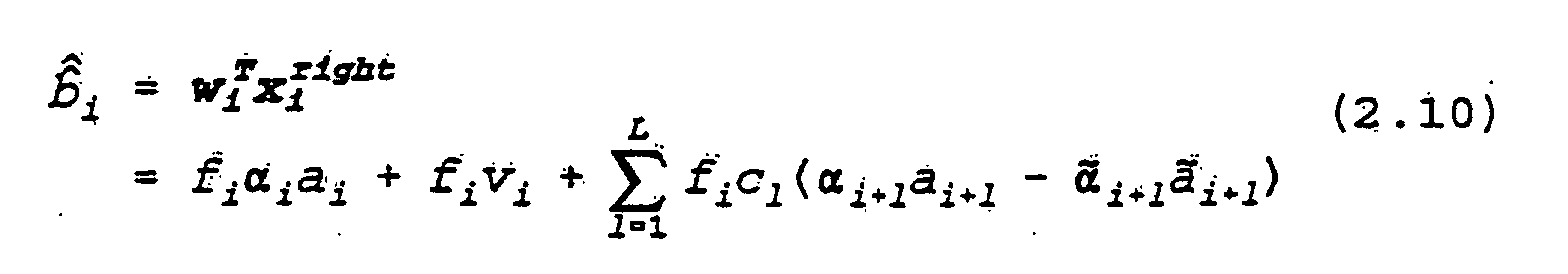
-
- The last term arises from any discrepancies in channel estimation and feedback decision errors. In comparison, the output of DP1 is given by equation (2.7) above.
- Figure 4 depicts the above described DFE structure with L = 2 feedback taps. This structure bears similarity with DFE structures used in a classical PRS system. This is not surprising because of the basic mathematical similarity in terms of time-frequency duality in the two approaches, notwithstanding the different motivations behind these techniques. Single-carrier PRS equalizers/detectors operate in the time-domain with symbol-spaced taps while the DFE here operates in the frequency-domain with bin-spaced taps. A key difference is that the effect of the channel (αi) is taken into account in the DFE here while this is not an issue in PRS equalizers.
- Figure 5 plots four different FDW window responses - Rectangular (only c0 = 1), Hanning (c0 = 1, c1 = -2, c2 = 1), Asymmetric FDW with non-zero coefficients (c0 = 1, c1 = -0.5) and with coefficients (c0 = 1, c1 = -1). There are, of course, a variety of other windows that may be used as well. It is seen that among the above windows the Hanning window displays the best side-lobe suppression. However, it also requires 2 feedback taps and has the largest SNR degradation in white noise of
10log 106=7.78 dB. In comparison, the last two windows have higher side-lobes but require only a single feedback tap and have white noise SNR degradations of 10log 101.25 = 0.97 dB and10log 102 = 3 dB respectively. - An alternate implementation of FDW can also be equivalently carried out after the FEQ stage in DP1, i.e., as

- See Fig. 5A. Fig. 5A shows the alternative demodulator architecture with frequency domain windowing. Following the
TEQ 32 and CP removerstage 34, the output of theCP remover 34 is provided to Fast Fourier Transform 120''. The output of the FFT 120'' in first data path 100'' is provided to the frequency domain equalizer (FEQ) 140''. The output of the FEQ 140'' represent the equalized subsymbols. The equalized subsymbols are provided to the bin select logic stage 300'' whose output is provided to the slicer 400''. The equalized subsymbols
 are also provided into the second data path 200'' comprising the frequency domain window stage 220'' and the decision feedback equalizer (DFE) 260''. The equalized subsymbols
 output from the DFE 260'' are provided to the bin select logic 300''. As in the other embodiments, the bin select logic selects the output from either the first path 100'' or the second path 200'' depending upon set criterion, e.g., which path produces more data bits per symbol or has a higher SNR. As in the other embodiments, the output from the slicer 400'' is provided in a feedback path to the DFE 260'' to cancel interference created by the frequency domain window stage 220''.
- Using equation (2.11) instead of (2.4), the corresponding DFE and input vectors from the embodiment of Fig. 5A are given as
- Thus, using wi and xi right from equation (2.12) above instead of equations (2.8) and (2.9), the equalized sub-symbols output from DP2 in the embodiment of Fig. 5A are given by

- Minor differences can be observed in the additive noise terms in equations (2.10) and (2.13). Instead of each post-FFT noise sample (u i+1 ) for the ith bin being weighted by fi , each is weighted by the corresponding FEQ coefficient (fi + 1 ). The resulting difference in the corresponding noise variances will be pronounced only if there are large differences between the channel attenuation coefficients over the DFE span. It is conceivable that this alternate FDW and DFE structure may be preferable in some implementations. This alternate DFE structure is applicable only to FDW while the previous DFE structure is applicable for both TDW as well as FDW and is used in the rest of this specification.
- During normal operation, ã i elements in xi right (or xi left) are obtained as reconstructed sub-symbol values obtained from the slicer. Care must be taken to normalize the
slicer 400, 400', 400'' output by taking the ADSL gain scaling factors and constellation energy normalization scaling factors into account before substituting them back into xi. The bin-select logic 300, 300', 300'' (Figures 1, 2 and 5A) determines the data-path (DP1 or DP2) used to provide the slicer input for any given sub-symbol.(Figure 4 shows slicer operating on). The bin-select logic may select all sub-symbols from DP1 only (i.e., no windowing is used), all from DP2 only, or select from DP1 or DP2 on a bin by bin basis. For example, in a simulation described below, a simple criterion of selecting the path which yields higher number of bits in a given bin is used. Once a SNR-per-bin profile is computed for DP1 and DP2, the bit-loading algorithm is run twice - once on each profile from DP1 and DP2. This ensures that the basic bit-loading algorithm being used need not be modified and that the combined bit-allocation is no worse than a conventional receiver having path DP1 only.
- A symbol-rate LMS update of FEQ (and thus, the DFE) weights can be carried out to track variations in the channel impulse response (CIR) and interference. Sub-rate adaptation may also be used for economy of implementation. Normalized LMS is preferred over regular LMS to make the adaptation speed impervious to the dynamic range of the input data for all bins.
- For DP1, the probability of symbol error per dimension for M2-ary QAM (Quadrature Amplitude Modulation) with AWGN is given byand dmin,i = |αi |d denotes the minimum distance between QAM constellation points at the channel output and d equals the distance between uncoded input QAM constellation points. For ADSL systems, the probability of symbol error per dimension (Pe/2) is generally specified (le-7 for ADSL/ADSL-Lite). Similarly, for DP2, using equations (2.10) and (2.14),
 This expression is highly intractable to evaluate for general cases when there are feedback decision errors. If error propagation is ignored and αi estimates are exact, equation (2.15) reduces to equation (2.14) with σu replaced by σv. Clearly, DFE performance will be degraded by feedback errors and it is important to take its effect into account in devising the overall equalization structure. Any errors are also likely to propagate through multiple bins because of the typically large values of feedback coefficients and increase the BER (bit error rate) from the specified value. However, owing to symbol-by-symbol detection in DMT, propagating errors are always confined to the same DMT symbol. Note that for a given SNR, Pe,DFE is increased compared to Pe due to possible error propagation in addition to any differences between σu and σv (which can additionally increased/decrease this difference). For the case of AWGN only, σ2 v ≥ σ2 u (equation 2.5) and Pe can be looked upon as a lower bound on Pe,DFE
- It is known that error propagation increases the probability of symbol error by at most a factor of ML where L is the number of feedback taps and when all symbols (symbol being equalized and feedback symbols) are M-ary PAM (Phase Amplitude Modulation). For example, letting Pe,DFE < KepPe, for a DFE with 1 feedback tap and 256QAM (M = 16), Kep =16. For a Hanning window with 2 feedback taps, Kep = 256. This expression also holds approximately for M2-ary QAM above when the cℓ coefficients are real resulting in IBI that is only between in-phase samples and only between quadrature samples. If the c1 are complex (for real asymmetric windows), there will be crosstalk between in-phase and quadrature samples and the above upper bound will be optimistic.
- The upper bound increases exponentially with the number of feedback taps. In general, the BER increases are large when there are multiple feedback coefficients (large L), the feedback coefficients have relatively large values (c1/c0 ratios are not small) and when multiple bits are loaded per sub-symbol (large M). There are some important differences between the problem at hand and the underlying assumptions of the above results. First, adjacent sub-symbols in DMT can belong to different sized constellations, i.e. different values of M for adjacent (feedback) bins. This further complicates a potential analytical solution for equation (2.15). Second, DMT symbols enjoy the benefit of deterministic pilot sub-symbols each symbol time, e.g. bin 64 downstream and
bin 16 upstream in T1.413). This puts a hard-limit on the extent of a single error propagation event. Finally, the upper bound above holds for AWGN only which is not the case of primary interest since windowing is useful only for cases with crosstalk and/or NBI. Nevertheless, the upper bound provides a valuable indicator for the performance degradation that can be expected. - The use of precoding to counter error propagation is well known in the literature. However, for the problem at hand, this approach suffers from some drawbacks. First, it requires participation of the transmitter. This precludes an independent application of the overall technique unless standardization considerations are met. Second, precoding does not necessarily provide immunity against error propagation depending on the constellation size and feedback coefficients. In fact, it has been shown to even marginally degrade performance for some cases. Third, the precoder is likely to be far more complex than the conventional precoders used in PRS systems. This is because the effect of channel coefficients and unequal QAM constellations in adjacent feedback bins has to be explicitly taken into account.
- An alternative (non-precoding, receiver-only) two-fold solution to this problem is to:
- (A) Provide an additional SNR Margin while doing bit-loading according to the achieved SNR in DP2 during training. In other words, the bit-allocation can be done for a BER which absorbs the effect of Kep. For example, bit-allocation in DP2 may be chosen to compensate for Kep = 100 (or more) by setting the target BER to be le-9 instead of le-7 with the 4 dB margin unchanged. Bit-allocation according to a lower target BER is equivalent to a "DFE SNR penalty" which can be calculated from BER versus SNR curves for QAM. For QAM sub-symbols and AWGN, the SNR penalty is 1.14 dB for this case (SNR penalty for le-10 BER specification is 1.62 dB).
- (B) Periodic Pseudo-Pilots can be established to reduce the threat of runaway errors within a symbol. A pseudo-pilot is defined as a bin which is provided an additional SNR margin, of say 3 dB (roughly equivalent to a reduction in 1 bit) to significantly reduce the probability of incurring an error and is demodulated using DP1. Pseudo-pilots can be established in several ways, such as periodically (such as every 32nd bin) or within groups of bins being decoded using DP2 (after bin-selection logic is done). Pseudo-pilots "reset" the decision feedback process while sequentially equalizing sub-symbols using the DFE. It would also permit equalization of groups of bins in parallel if desired, where each group is equalized sequentially using its pseudo-pilot as the reference starting sub-symbol. If 2 or more feedback taps are used, the number of pseudo-pilots required also increases proportionally, e.g. pairs of adjacent pseudo-pilots are required for a Hanning window requiring 2 feedback decisions.
-
- These measures will reduce the aggregate data rate that can be achieved by the use of windowing. It is also preferable to minimize the number of feedback coefficients since it reduces computation as well as the risk of error propagation (or reduced SNR penalty).
- Test cases are presented in Figures 7 - 13 for downstream transmission. Figure 6 depicts the two example loops used for the plots. The first loop (ANSI T1.601 loop 2) is 16.5 Kft with one bridge tap. The second loop (CSA Loop 4) is a medium length 7.6 Kft loop with 2 bridge taps. The NBI is generated simply by a tonal interferer (cosine) whose angular frequency wc randomly changes every 100 DMT symbols for b ∈ [bc-1, bc + 1] where Wb = 2πb/2N and bc = 50 for Figure pairs 7, 8 and 9, 10. Downstream parameters are N = 256, G = 32, fs = 2.208 MHz and only bins 33-127 active. A Least Squares based channel shortening TEQ algorithm with channel estimation was used in all cases to shorten the CIR except in Figure 13. Channel estimation was performed using impulse trains in the presence of the impairments such as crosstalk or NBI. With 544 samples/symbol, the 10-tap FIR TEQ filter requires 5,440 real multiplications and 4896 real additions per DMT symbol time.
- A 2-tap FDW (Window 1) and a 3-tap Hanning window (Window 2) are used for all cases shown with bin 64 (pilot) as the reference bin. For the Hanning window, bin 63 is also used as a reference to initiate the equalization process. For bin indices greater than 64, the DFE input vector is Xi right while Xi left is used for the others. The window feedback coefficients are appropriately chosen. For example, for
Window 1, the coefficients are c0 = 1, c1 = - 1 for bin index greater than 64 and c0 = 1, c-1 = -1 for bin index less than 64. Similarly, forwindow 2, the coefficients are c0 = 1, c+1 = - 2, c+2 = 1 for bin index greater than 64 and c0 = 1, c-1 = -2, c-2 = 1 for bin index less than 64.Window 1 is seen to provide a good trade-off between having fewer feedback taps, good side-lobe suppression and low SNR degradation in white noise. The spikes seen in the bit-allocation plots at bin 64 are due to the pilot bin which is always modulated with a constant 2-bit sub-symbol. For comparison, the SNR is also plotted for a symmetric Hanning window (c0 = 1, c-1 = - 0.5, c1 = -0.5) with only alternate bins active. To achieve this, the gain-scaling factor on alternate bins is set to zero at the transmitter. This ensures that there is no IBI between adjacent bins and only a single-tap FEQ (as in DP1) is required. This, of course, also reduces the number of active bins by half but can serve as a good indication of what is potentially achievable through windowing. - For these cases, the signal and noise (crosstalk or NBI) PSD's are plotted before and after the channel shortening TEQ. AWGN of PSD -140 dBm/Hz is added to the crosstalk and NBI for all cases. It can be seen that the TEQ alters the spectrum of the signal and noise at the input of DP1 and DP2 and thus influences the performance of the rest of the receiver. The achieved SNR per bin is plotted for the conventional method (identical to DP1) and with windowing (DP2). The resulting bit-loading tables depict the resulting bit loading profiles for le-7 BER with 4 dB margin for DP1 and using Window 1 (bit-loading arising from
Window 2 is not plotted). Bit-loading for DP2 also includes an additional SNR margin of 1.14 dB as described above. The bin-select logic for selecting DP1 or DP2 for any given bin is simply to select the path which yields higher bits per bin after bit-loading is complete. In case of a tie, DP1 is chosen. The combined (maximum) bit allocation is marked by "circles".Example cases plotted in Figures 7- 13. FIGURE Loop Crosstalk NBI TEQ 7, 8 Long -- Yes Yes 9, 10 Medium -- Yes Yes 11, 12 Medium 10 ADSL-US -- Yes 13 Medium 10 ADSL-US -- -- - Figures 7 and 8 show that the DFE provides the most gain in the vicinity of the NBI.
Window 2 performs better thanWindow 1 in the immediate vicinity of the NBI but incurs a greater loss in the rest of the band. The effect of NBI monotonically reduces with frequency separation. Thus, bins spaced further in frequency are less affected and the performance advantage of windowing gradually reduces until it approaches the white-noise loss of 3 dB forWindow 1. Figures 9 and 10 display similar performance for the medium loop. It is notable that performance gains are dependent on the strength of the NBI relative to the ambient SNR determined by the received signal power after passing through the channel and the AWGN floor. In Figure 9, the effect of the NBI is more pronounced compared to Figure 7 because the ambient SNR is higher. Thus, NBI suppression is more effective and greater gains are obtained via windowing. - Figures 11 and 12 show that the DFE provides no advantage in the presence of crosstalk which is not strongly colored after the TEQ (Time Domain Equalizer). In fact, in the latter portion of the spectrum where the noise is mainly spectrally flat white,
Windows - The extra computation in DP2 arises from two main things - windowing and the DFE. Table B shows these requirements for
Window 1 for downstream (at ATU-R) and upstream (at ATU-C) channels in'terms of multiplications and additions required per DMT symbol (Aggregate symbol rate is 4 KHz in ADSL standards). The assumed parameters are: - (A) Downstream: N = 256 or 128, ATU-R performs 2N point FFTs, 95 bins active (33-127).
- (B) Upstream: N = 32, ATU-C performs 64 point FFTs, 26 bins active (6-31).
- (C) FDW: complex additions and L + 1 complex multiplications with the channel coefficients, (assuming window coefficients can be implemented as binary shift operations).
- (D) DFE: L complex additions and (L + 1)
complex multiplications per symbol.
Additional real (multiplications, additions) per DMT symbol with 2-tap FDW and DFE (Figure 4(B)). Location FDW DFE ATU-R (N=128 or 256) 0, 380 760,190 ATU-C(N=32) 0, 104 208,52 -
- The TDW operation requires 2N real multiplications when a 2N-pt FFT is used while the DFE complexity is the same as above. However, most of the additional complexity lies in doing an extra FFT. Optimized implementations of FFT's often incur fewer multiplications/additions than shown above by exploiting the fact that the input is purely real and only the first N outputs are required (output is conjugate symmetric).
- While TDW and FDW are equivalent, there can be a significant difference in computational load. All windows with real coefficients result in equal TDW complexity. On the other hand, the computational load in FDW depends on the number of feedback coefficients, i.e. on the particular FDW frequency response. Also, FDW is independent of the preceding FFT size and can be carried out on a bin-by-bin basis as required. Provision for implementing multiple windows can be done by making the number of FDW coefficients and their values programmable. Furthermore, different bins can have different windows applied to them (in the same symbol) if desired, (including no windowing). In the case of TDW, the window coefficients can be programmable as well and FFT blocks used in other algorithms (such as for the TEQ or for PAR (Peak-to-Average Ratio) reduction) may be available for reuse. Alternative embodiments of TDW can potentially be used to reduce the implementation complexity in terms of hardware and/or required instructions. For instance, the two FFT's in Figure 1 can be executed by the same hardware/firmware block in a sequential fashion (staggered in time) instead of being done simultaneously by two different blocks.
- Among different windows, 2-tap FDWs (1 feedback tap) are well-suited since they provide a good balance between side-lobe suppression and complexity. Windows with multiple feedback taps suffer from the drawbacks of increased risk of error propagation, need for greater number of reference sub-symbols and greater DFE computation. Also, depending on the feedback tap values, the SNR degradation in white noise only is also greater. For example, the window with coefficients c0 = 1, c1 = -1
loses 3 dB in white noise while the Hanning window (c0 = 1, c1 = -2, c2 = 1) loses 7.78 dB. In general, this implies that to obtain noise suppression benefits, the interference has to have much stronger correlation and thus is well suited only for a limited number of cases. DPS windows are a class of windows which can be tailored for different side-lobe suppression versus main-lobe width trade-off at the expense of greater number of DFE taps (Figure 3) and can be used in some situations. - The FEQ and DFE can adapt to NBI and/or crosstalk if it emerges sufficiently slowly relative to the tracking capabilities of the LMS (Least Mean Squares) algorithm and change the bit-allocation via bit-swaps. More elaborate and potentially faster tracking RLS (Recursive Least Squares) algorithms may also be used. If a strong interferer appears suddenly, the modem may fall back into fast retrain (in ADSL-Lite) or even a full restart. In any case, the sustainable data rate (or SNR margin) after the incident is likely to be better, or equivalently require fewer bit-swaps.
- There is a trade off between greater loop reach, SNR Margin or data-rate. This follows from the fact that, depending on the operative constraints, a higher achievable SNR in bins is equivalent to (A) Greater loop reach for a given minimum margin and data rate or (B) Higher SNR margin in active data carrying bins for a given data-rate and loop reach or (C) Greater data-rate for a given reach and margin. Gains in SNR using the invention are not unconditional, i.e., gains may be realized only in the presence of NBI, highly correlated crosstalk, or other imperfections such as inadequate channel shortening, symbol alignment offsets and jitter.
- Discounting minor changes, the overall technique is likely to be applicable to other DMT based modems such as VDSL and wireless OFDM as well. NBI and other impairments discussed above are known to afflict wireless and VDSL systems also, perhaps even more so. These modems uses a transmitter PMD (Physical Media Dependent) structure largely similar to that in ADSL modems considered above. Moreover, since transmitter participation is not required for this technique, most standard-compatibility related issues are rendered irrelevant.
- Although the present invention has been described in relation to particular embodiments thereof, many other variations and modifications and other uses will become apparent to those skilled in the art. Therefore, the present invention should be limited not by the specific disclosure herein, but only by the appended claims.
Claims (46)
- A receiver providing a demodulated output (ã) from a received discrete multi-tone modulated input signal, the input signal received from a communication channel having noise thereon, the input signal having modulated thereon a digital bit stream, the receiver comprising:first (100, 100', 100") and second (200, 200', 200") data paths coupled to receive the input signal;the first of the two data paths (100, 100', 100") comprising a first stage having a frequency response for applying a discrete Fourier Transform (120, 120', 120") to the input signal and further comprising a frequency domain equalizer (140, 140', 140") having an input coupled to an output of the first stage;the second of the two data paths (200, 200', 200") comprising a window stage (220, 220', 220") for suppressing side lobes of the frequency response of the first stage; anda logic stage (300, 300', 300") for selecting an output from the first data path or the second data path based on a predefined test and for providing a selected output representing the demodulated digital bit stream.
- The receiver of claim 1, further comprising a decision feed back equalizer (260, 260', 260") in said second data path having as an input an output from said window stage and for cancelling inter-bin interference created by said window stage.
- The receiver of claim 2, wherein the decision feedback equalizer receives a feedback signal (410, 410', 410") from an output of said logic stage to cancel the inter-bin interference.
- The receiver of claim 3, further comprising a slicer stage (400, 400', 400") having as an input the output of said logic stage and providing as an output the demodulated digital bit stream (ã); said demodulated digital bit stream being provided as said feedback signal.
- The receiver of claim 1, 2, 3 or 4, wherein the window stage in said second path comprises a time domain window stage (220).
- The receiver of claim 5, wherein said time domain window stage has an input directly from a time domain equalizer.
- The receiver of claim 6, further comprising a second stage for performing a discrete Fourier transform (240) in said second path, the second stage having an input receiving an output from said time domain window stage.
- The receiver of claim 7, further comprising a decision feedback equalizer (260) in said second data path having an input from said second stage and having an output provided to said logic stage.
- The receiver of claim 8, wherein the decision feedback equalizer receives a further input (122) from said first stage.
- The receiver of any one of claims 1 to 4, wherein said window stage in the second data path comprises a frequency domain window stage (220', 220").
- The receiver of claim 10, further comprising a decision feedback equalizer (260', 260") in said second data path having an input receiving an output from said frequency domain window stage, said decision feedback equalizer being provided for cancelling inter-bin interference created by the frequency domain window stage; an output of said decision feedback equalizer being provided to said logic stage.
- The receiver of claim 11, further wherein the decision feedback equalizer (260') has a further input (142') from said first stage.
- The receiver of claim 12, wherein a feedback signal (410') is provided from an output of said logic stage to said decision feedback equalizer to cancel inter-bin interference created by said frequency domain window stage.
- The receiver of claim 13, wherein the logic stage (300') provides an output to a slicer stage (400') the slicer stage providing said demodulated digital bit stream as an output (ã), said feedback signal comprising said demodulated output.
- The receiver of claim 10, 11, 12, 13 or 14, wherein said frequency domain window stage has an input coupled to an output of said first stage.
- The receiver of any one of claims 1 to 15, wherein the logic stage (300, 300', 300") selects an output from the first data path or the second data path based on determining which data path provides more bits per symbol or has a higher signal to noise ratio.
- The receiver of claim 16, wherein in the event of a tie, the logic stage selects the first data path.
- The receiver of any one of claims 1 to 17, wherein the window stage comprises one of a Hanning window function, a DPS window function and a Bartlett window function.
- The receiver of any one of claims 5 to 9, wherein the time domain window stage (220) performs time domain pulse shaping by a sample-by-sample multiplication of the output from the time domain equalizer by window coefficients defining a time domain window function of the time domain window stage.
- The receiver of any one of claims 10 to 15, wherein the frequency domain window stage performs frequency domain pulse shaping on a bin-by-bin basis by performing a linear combination of bin outputs and frequency domain window coefficients defining a frequency domain window function of the frequency domain window stage.
- The receiver of any one of claims 1 to 20, wherein the frequency domain equalizer (140, 140', 140") comprises a one-tap per-bin equalizer.
- The receiver of any one of claims 1 to 21, further comprising a time domain equalizer (32) having as an input the input signal received from the communication channel, the time domain equalizer having an output provided to the first and second data paths.
- The receiver of any one of claims 10 to 15, wherein the window stage (220") has an input from an output of the frequency domain equalizer (140").
- A method of providing a demodulated output from a received discrete multi-tone modulated input signal, the input signal received from a communication channel having noise therein, the input signal having modulated thereon a digital bit stream, the method comprising:providing the input signal to first (100, 100', 100") and second (200, 200', 200") data paths;applying a discrete Fourier Transform (120, 120', 120") to the input signal in the first data path to generate a first transformed signal (142') and frequency domain equalizing (140, 140', 140") the first transformed signal to provide a frequency domain equalized signal;suppressing side lobes of the frequency response of the first transformed signal in the second data path by applying a window function (220, 220', 220") to provide a pulse shaped signal; andselecting (300, 300', 300") an output from the first data path or the second data path based on a predefined test and providing a selected output representing the demodulated digital bit stream.
- The method of claim 24, further comprising performing decision feed back equalizing (260, 260', 260") in said second data path on said pulse shaped signal for cancelling inter-bin interference created by said window function.
- The method of claim 25, further comprising during the step of decision feedback equalizing, providing a feedback signal (410, 410', 410") comprising the selected output to cancel the inter- bin interference.
- The method of claim 26, further comprising slicing (400, 400', 400") the selected output and providing the sliced output as the demodulated digital bit stream; said demodulated digital bit stream being provided as said feedback signal.
- The method of claim 24, 25, 26 or 27, wherein the step of applying a window function in said second path comprises applying a time domain window function (220).
- The method of claim 28, wherein said step of applying a time domain window function comprises applying a time domain window function directly to said input signal.
- The method of claim 29, further comprising performing a discrete Fourier transform (240) in said second path to provide a second transformed signal (b and), after said step of applying a time domain window function.
- The method of claim 30, further comprising performing decision feedback equalizing (260) in said second data path on said second transformed signal.
- The method of claim 31, further comprising using said first transformed signal (142') during the step of decision feedback equalizing (260).
- The method of any one of claims 24 to 27, wherein said step of applying a window function in the second data path comprises applying a frequency domain window function (220', 220").
- The method of claim 33, further comprising performing decision feedback equalizing (260', 260") in said second data path on said pulse shaped signal, said step of decision feedback equalizing being provided for cancelling inter-bin interference created by the frequency domain window function; and providing a decision feedback equalized signal () for selection as an output signal.

- The method of claim 34, further comprising using the first transformed signal (142') during said step of decision feedback equalizing (260").
- The method of claim 35, further comprising providing a feedback signal (410') during said step of decision feedback equalizing to cancel inter-bin interference created by said frequency domain window function.
- The mechod of claim 36, further comprising slicing (400) the selected output into the demodulated digital bit stream (ã), said feedback signal comprising said demodulated digital bit stream.
- The method of any one of claims 33 to 37, further comprising applying the frequency domain window function (220') to said first transformed signal.
- The method of any one of claims 24 to 38, wherein the step of selecting (300, 300', 300") an output from the first data path or the second data path comprises selecting an output based on determining which data path provides more bits per symbol or has a higher signal to noise ratio.
- The method of claim 39, wherein in the event of a tie, the step of selecting an output comprises selecting the first data path.
- The method of any one of claims 24 to 40, wherein the window function comprises one of a Hanning window function, a DPS window function, and a Bartlett window function.
- The method of any one of claims 28 to 32, wherein said step of applying a time domain window function comprises time domain pulse shaping by a sample-by-sample multiplication of the time domain equalized signal by window coefficients defining the time domain window function.
- The method of any one of claims 33 to 38, wherein the step of applying a frequency domain window function comprises frequency domain pulse shaping on a bin-by-bin basis by performing a linear combination of bin outputs and frequency domain window coefficients defining the frequency domain window function.
- The method of any one of claims 24 to 38, wherein the step of frequency domain equalizing (140, 140', 140") comprises frequency domain equalizing using a one-tap per-bin equalizer.
- The method of any one of claims 24 to 44, further comprising time domain eqalizing (32) the input signal received from the communication channel to produce a time domain equalized signal, and providing the time domain equalized signal to the first and second data paths.
- The method of any one of claims 33 to 38, further comprising applying the window function (220") to the frequency domain equalized signal ().

Applications Claiming Priority (2)
| Application Number | Priority Date | Filing Date | Title |
|---|---|---|---|
| US288478 | 1999-04-08 | ||
| US09/288,478 US7023938B1 (en) | 1999-04-08 | 1999-04-08 | Receiver for discrete multitone modulated signals having window function |
Publications (3)
| Publication Number | Publication Date |
|---|---|
| EP1043875A2 EP1043875A2 (en) | 2000-10-11 |
| EP1043875A3 EP1043875A3 (en) | 2002-04-03 |
| EP1043875B1 true EP1043875B1 (en) | 2004-07-28 |
Family
ID=23107276
Family Applications (1)
| Application Number | Title | Priority Date | Filing Date |
|---|---|---|---|
| EP99122054A Expired - Lifetime EP1043875B1 (en) | 1999-04-08 | 1999-11-17 | Receiver for discrete multitone modulated signals having window function |
Country Status (4)
| Country | Link |
|---|---|
| US (1) | US7023938B1 (en) |
| EP (1) | EP1043875B1 (en) |
| JP (1) | JP2000307481A (en) |
| DE (1) | DE69918945T2 (en) |
Families Citing this family (37)
| Publication number | Priority date | Publication date | Assignee | Title |
|---|---|---|---|---|
| SE9801748L (en) * | 1998-05-18 | 1999-11-19 | Telia Ab | Improvements in or relating to telecommunication transmission systems |
| US6563841B1 (en) * | 1999-08-30 | 2003-05-13 | Nec Usa, Inc. | Per-bin adaptive equalization in windowed DMT-type modem receiver |
| AU2757701A (en) | 1999-12-30 | 2001-07-16 | Bandspeed, Inc. | Approach for processing data received from a communications channel in finite precision arithmetic applications |
| ATE357802T1 (en) | 2000-04-18 | 2007-04-15 | Aware Inc | DATA ASSIGNMENT WITH CHANGEABLE SIGNAL-NOISE RATIO |
| US6996199B2 (en) * | 2001-01-25 | 2006-02-07 | Bandspeed, Inc. | Approach for processing data received from a communications channel to reduce noise power and optimize impulse response length to reduce inter-symbol interference and inter-channel interference |
| US7272199B2 (en) | 2001-01-25 | 2007-09-18 | Bandspeed, Inc. | Adaptive adjustment of time and frequency domain equalizers in communications systems |
| US7023937B2 (en) * | 2001-03-01 | 2006-04-04 | Texas Instruments Incorporated | Receiver window design for multicarrier communication systems |
| US6856649B2 (en) * | 2001-03-30 | 2005-02-15 | Koninklijke Philips Electronics N.V. | Initialization scheme for a hybrid frequency-time domain equalizer |
| US7042937B2 (en) * | 2001-04-23 | 2006-05-09 | Koninklijke Philips Electronics N.V. | Hybrid frequency-time domain equalizer |
| US7274736B2 (en) * | 2001-10-24 | 2007-09-25 | Texas Instruments Incorporated | Multiple path equalization for multicarrier systems |
| US7263119B1 (en) * | 2001-11-29 | 2007-08-28 | Marvell International Ltd. | Decoding method and apparatus |
| DE10160733A1 (en) * | 2001-12-11 | 2003-08-28 | Siemens Ag | Method for the continuous estimation of the equalization coefficients for wired transmission systems |
| US7139343B2 (en) * | 2002-03-27 | 2006-11-21 | Hitachi Kokusai Electric Inc. | Digital radio receiver |
| WO2003090422A1 (en) * | 2002-04-19 | 2003-10-30 | Conexant Systems, Inc. | System and method for detecting narrowband interference in a wideband ofdm sign al based on normalized subcarrier amplitudes |
| TW200401522A (en) * | 2002-05-17 | 2004-01-16 | Matsushita Electric Ind Co Ltd | Receiving device and receiving method and transmission path characteristic measurement device |
| US7453949B2 (en) * | 2003-12-09 | 2008-11-18 | Agere Systems Inc. | MIMO receivers having one or more additional receive paths |
| JP4199144B2 (en) * | 2004-03-11 | 2008-12-17 | 株式会社東芝 | Weight function generation device, reference signal generation device, transmission signal generation device, signal processing device, and antenna device |
| US7477683B2 (en) * | 2004-03-29 | 2009-01-13 | Stmicroelectronics Ltd. | Periodic DMT signals with cyclic extension |
| CN100571111C (en) * | 2004-12-28 | 2009-12-16 | 中兴通讯股份有限公司 | Be used for the method disturbed between the suppressed carrier of OFDM mobile communication system |
| JP4675790B2 (en) * | 2006-01-27 | 2011-04-27 | 三菱電機株式会社 | Communication apparatus and communication system |
| KR101200736B1 (en) * | 2006-03-14 | 2012-11-13 | 퀄컴 인코포레이티드 | Apparatus and method for transmitting and receiving packet data in a smart antenna system |
| JP5248507B2 (en) * | 2006-09-15 | 2013-07-31 | イカノス・コミュニケーションズ・インコーポレーテッド | Method and apparatus for robustness of differentiated communication channels in multitone transceivers |
| GB0707355D0 (en) * | 2007-04-16 | 2007-05-23 | Nxp Bv | Channel estimation |
| US8321491B2 (en) * | 2007-06-26 | 2012-11-27 | The United States Of America As Represented By The Secretary Of The Army | System and method for detecting a weak signal in a noisy environment |
| US8321823B2 (en) * | 2007-10-04 | 2012-11-27 | Carnegie Mellon University | System and method for designing architecture for specified permutation and datapath circuits for permutation |
| JP4875642B2 (en) * | 2008-02-27 | 2012-02-15 | 株式会社日立製作所 | Noise power estimation apparatus and method |
| US8295395B2 (en) * | 2008-09-30 | 2012-10-23 | Apple Inc. | Methods and apparatus for partial interference reduction within wireless networks |
| TWI416955B (en) * | 2008-11-24 | 2013-11-21 | Realtek Semiconductor Corp | Single-carrier/multi-carrier community receiver and method for processing signal received by signle-carrier/multi-carrier community receiver |
| CN101808059B (en) * | 2009-02-13 | 2013-04-24 | 瑞昱半导体股份有限公司 | Single carrier/multi-carrier share receiver |
| EP2228955B1 (en) | 2009-03-13 | 2017-02-22 | OCT Circuit Technologies International Limited | System and method for OFDM reception in the presense of Doppler effect based on time domain windowing |
| US8755460B2 (en) * | 2010-07-30 | 2014-06-17 | National Instruments Corporation | Phase aligned sampling of multiple data channels using a successive approximation register converter |
| US8804809B2 (en) | 2011-09-12 | 2014-08-12 | Transwitch Corporation | Techniques for setting feedback coefficients of a PAM-N decision feedback equalizer |
| US8908796B1 (en) * | 2013-05-15 | 2014-12-09 | University Of South Florida | Orthogonal frequency division multiplexing (OFDM) transmitter and receiver windowing for adjacent channel interference (ACI) suppression and rejection |
| US8971396B1 (en) | 2013-08-22 | 2015-03-03 | Pmc-Sierra Us, Inc. | Windowed-based decision feedback equalizer and decision feedback sequence estimator |
| WO2015067990A1 (en) | 2013-11-06 | 2015-05-14 | Freescale Semiconductor, Inc. | FFT device and method for performing a Fast Fourier Transform |
| JP6935370B2 (en) * | 2018-07-24 | 2021-09-15 | アンリツ株式会社 | Signal generator and frequency characteristic display method using the device |
| CN109871575B (en) * | 2018-12-29 | 2022-12-20 | 陕西海泰电子有限责任公司 | Electromagnetic interference receiver window function design method based on time domain FFT |
Family Cites Families (7)
| Publication number | Priority date | Publication date | Assignee | Title |
|---|---|---|---|---|
| KR100331437B1 (en) * | 1995-06-30 | 2002-08-08 | 삼성전자 주식회사 | Adaptive bit switch apparatus of dmt system and method thereof |
| FR2743967B1 (en) * | 1996-01-18 | 1998-03-27 | France Telecom | METHOD AND DEVICE FOR TIME SYNCHRONIZATION OF A RECEIVER OF A MULTI-CARRIER SIGNAL |
| US6014412A (en) * | 1996-04-19 | 2000-01-11 | Amati Communications Corporation | Digital radio frequency interference canceller |
| EP0802649A1 (en) * | 1996-04-19 | 1997-10-22 | ALCATEL BELL Naamloze Vennootschap | Method and windowing unit to reduce leakage, Fourier transformer and DMT modem wherein the unit is used |
| US6353629B1 (en) * | 1997-05-12 | 2002-03-05 | Texas Instruments Incorporated | Poly-path time domain equalization |
| US6047025A (en) * | 1998-02-13 | 2000-04-04 | Motorola, Inc. | Method and apparatus for equallization in an asymmetric digital aubscriber line communications system |
| US6396886B1 (en) * | 1999-02-12 | 2002-05-28 | Nec Usa, Inc. | DMT time-domain equalizer algorithm |
-
1999
- 1999-04-08 US US09/288,478 patent/US7023938B1/en not_active Expired - Fee Related
- 1999-11-17 EP EP99122054A patent/EP1043875B1/en not_active Expired - Lifetime
- 1999-11-17 DE DE69918945T patent/DE69918945T2/en not_active Expired - Lifetime
-
2000
- 2000-02-14 JP JP2000034721A patent/JP2000307481A/en not_active Withdrawn
Also Published As
| Publication number | Publication date |
|---|---|
| DE69918945T2 (en) | 2004-12-16 |
| EP1043875A2 (en) | 2000-10-11 |
| JP2000307481A (en) | 2000-11-02 |
| DE69918945D1 (en) | 2004-09-02 |
| EP1043875A3 (en) | 2002-04-03 |
| US7023938B1 (en) | 2006-04-04 |
Similar Documents
| Publication | Publication Date | Title |
|---|---|---|
| EP1043875B1 (en) | Receiver for discrete multitone modulated signals having window function | |
| Benvenuto et al. | On the comparison between OFDM and single carrier modulation with a DFE using a frequency-domain feedforward filter | |
| US6266367B1 (en) | Combined echo canceller and time domain equalizer | |
| US6097763A (en) | MMSE equalizers for DMT systems with cross talk | |
| US6549512B2 (en) | MDSL DMT architecture | |
| EP0933897B1 (en) | Reduction of interference in duplex discrete multitone communications systems | |
| US8265215B1 (en) | Method and system for determining symbol boundary timing in a multicarrier data transmission system | |
| JP2007195218A (en) | Digital radio frequency interference canceller | |
| US6452987B1 (en) | Fast start-up in discrete multi-tone (DMT) based communications system | |
| US8170125B2 (en) | Subdimensional single-carrier modulation | |
| JPH11196060A (en) | Multi-band detector | |
| KR100441250B1 (en) | Method for calculating coefficients of equalizer and device for calculating the same | |
| US7817730B2 (en) | Training sequence for symbol boundary detection in a multicarrier data transmission system | |
| US6563841B1 (en) | Per-bin adaptive equalization in windowed DMT-type modem receiver | |
| US8385399B2 (en) | Method for impulse noise mitigation | |
| US7289554B2 (en) | Method and apparatus for channel equalization and cyclostationary interference rejection for ADSL-DMT modems | |
| US20050111538A1 (en) | Method and apparatus for improving the quality of channel estimation algorithms using training sequences | |
| Kapoor et al. | Interference suppression in DMT receivers using windowing | |
| US20110228838A1 (en) | Apparatus for impulse noise mitigation | |
| Milosevic et al. | DMT bit rate maximization with optimal time domain equalizer filter bank architecture | |
| Zeng et al. | Near-end crosstalk mitigation in ADSL systems | |
| US7274736B2 (en) | Multiple path equalization for multicarrier systems | |
| Ding et al. | An achievable performance upper bound for discrete multitone equalization | |
| Shim et al. | Complexity analysis of multicarrier and single-carrier systems for very high-speed digital subscriber line | |
| Khan et al. | Channel equalization for Discrete Wavelet Multitone transceiver in wireline channels |
Legal Events
| Date | Code | Title | Description |
|---|---|---|---|
| PUAI | Public reference made under article 153(3) epc to a published international application that has entered the european phase |
Free format text: ORIGINAL CODE: 0009012 |
|
| AK | Designated contracting states |
Kind code of ref document: A2 Designated state(s): AT BE CH CY DE DK ES FI FR GB GR IE IT LI LU MC NL PT SE Kind code of ref document: A2 Designated state(s): DE GB |
|
| AX | Request for extension of the european patent |
Free format text: AL;LT;LV;MK;RO;SI |
|
| PUAL | Search report despatched |
Free format text: ORIGINAL CODE: 0009013 |
|
| AK | Designated contracting states |
Kind code of ref document: A3 Designated state(s): AT BE CH CY DE DK ES FI FR GB GR IE IT LI LU MC NL PT SE |
|
| AX | Request for extension of the european patent |
Free format text: AL;LT;LV;MK;RO;SI |
|
| RIC1 | Information provided on ipc code assigned before grant |
Free format text: 7H 04L 27/26 A, 7H 04L 1/00 B |
|
| 17P | Request for examination filed |
Effective date: 20020220 |
|
| AKX | Designation fees paid |
Free format text: DE GB |
|
| GRAP | Despatch of communication of intention to grant a patent |
Free format text: ORIGINAL CODE: EPIDOSNIGR1 |
|
| GRAS | Grant fee paid |
Free format text: ORIGINAL CODE: EPIDOSNIGR3 |
|
| GRAA | (expected) grant |
Free format text: ORIGINAL CODE: 0009210 |
|
| AK | Designated contracting states |
Kind code of ref document: B1 Designated state(s): DE GB |
|
| REG | Reference to a national code |
Ref country code: GB Ref legal event code: FG4D |
|
| REG | Reference to a national code |
Ref country code: IE Ref legal event code: FG4D |
|
| REF | Corresponds to: |
Ref document number: 69918945 Country of ref document: DE Date of ref document: 20040902 Kind code of ref document: P |
|
| REG | Reference to a national code |
Ref country code: GB Ref legal event code: 711B |
|
| REG | Reference to a national code |
Ref country code: GB Ref legal event code: 711G |
|
| PLBE | No opposition filed within time limit |
Free format text: ORIGINAL CODE: 0009261 |
|
| STAA | Information on the status of an ep patent application or granted ep patent |
Free format text: STATUS: NO OPPOSITION FILED WITHIN TIME LIMIT |
|
| 26N | No opposition filed |
Effective date: 20050429 |
|
| REG | Reference to a national code |
Ref country code: GB Ref legal event code: 732E Free format text: REGISTERED BETWEEN 20090917 AND 20090923 |
|
| PGFP | Annual fee paid to national office [announced via postgrant information from national office to epo] |
Ref country code: DE Payment date: 20091112 Year of fee payment: 11 |
|
| PGFP | Annual fee paid to national office [announced via postgrant information from national office to epo] |
Ref country code: GB Payment date: 20091111 Year of fee payment: 11 |
|
| GBPC | Gb: european patent ceased through non-payment of renewal fee |
Effective date: 20101117 |
|
| REG | Reference to a national code |
Ref country code: DE Ref legal event code: R119 Ref document number: 69918945 Country of ref document: DE Effective date: 20110601 Ref country code: DE Ref legal event code: R119 Ref document number: 69918945 Country of ref document: DE Effective date: 20110531 |
|
| PG25 | Lapsed in a contracting state [announced via postgrant information from national office to epo] |
Ref country code: DE Free format text: LAPSE BECAUSE OF NON-PAYMENT OF DUE FEES Effective date: 20110531 |
|
| PG25 | Lapsed in a contracting state [announced via postgrant information from national office to epo] |
Ref country code: GB Free format text: LAPSE BECAUSE OF NON-PAYMENT OF DUE FEES Effective date: 20101117 |