EP1043165A1 - Thermal print head and method of manufacturing the same - Google Patents
Thermal print head and method of manufacturing the same Download PDFInfo
- Publication number
- EP1043165A1 EP1043165A1 EP98954810A EP98954810A EP1043165A1 EP 1043165 A1 EP1043165 A1 EP 1043165A1 EP 98954810 A EP98954810 A EP 98954810A EP 98954810 A EP98954810 A EP 98954810A EP 1043165 A1 EP1043165 A1 EP 1043165A1
- Authority
- EP
- European Patent Office
- Prior art keywords
- substrate
- protective film
- longitudinal side
- thermal printhead
- heating elements
- Prior art date
- Legal status (The legal status is an assumption and is not a legal conclusion. Google has not performed a legal analysis and makes no representation as to the accuracy of the status listed.)
- Granted
Links
- 238000004519 manufacturing process Methods 0.000 title description 3
- 239000000758 substrate Substances 0.000 claims abstract description 100
- 230000001681 protective effect Effects 0.000 claims abstract description 69
- 238000010438 heat treatment Methods 0.000 claims abstract description 26
- 238000000034 method Methods 0.000 claims description 11
- 239000010408 film Substances 0.000 description 69
- 239000010410 layer Substances 0.000 description 57
- 239000004020 conductor Substances 0.000 description 12
- 230000003064 anti-oxidating effect Effects 0.000 description 11
- 244000126211 Hericium coralloides Species 0.000 description 6
- 238000005229 chemical vapour deposition Methods 0.000 description 6
- 239000010409 thin film Substances 0.000 description 5
- 239000011241 protective layer Substances 0.000 description 4
- 238000000151 deposition Methods 0.000 description 3
- PBCFLUZVCVVTBY-UHFFFAOYSA-N tantalum pentoxide Inorganic materials O=[Ta](=O)O[Ta](=O)=O PBCFLUZVCVVTBY-UHFFFAOYSA-N 0.000 description 3
- PNEYBMLMFCGWSK-UHFFFAOYSA-N Alumina Chemical compound [O-2].[O-2].[O-2].[Al+3].[Al+3] PNEYBMLMFCGWSK-UHFFFAOYSA-N 0.000 description 2
- 229910052581 Si3N4 Inorganic materials 0.000 description 2
- VYPSYNLAJGMNEJ-UHFFFAOYSA-N Silicium dioxide Chemical compound O=[Si]=O VYPSYNLAJGMNEJ-UHFFFAOYSA-N 0.000 description 2
- 229910010293 ceramic material Inorganic materials 0.000 description 2
- 238000005530 etching Methods 0.000 description 2
- 239000011521 glass Substances 0.000 description 2
- 238000010348 incorporation Methods 0.000 description 2
- 239000011810 insulating material Substances 0.000 description 2
- 239000000463 material Substances 0.000 description 2
- XMQFTWRPUQYINF-UHFFFAOYSA-N bensulfuron-methyl Chemical compound COC(=O)C1=CC=CC=C1CS(=O)(=O)NC(=O)NC1=NC(OC)=CC(OC)=N1 XMQFTWRPUQYINF-UHFFFAOYSA-N 0.000 description 1
- 229910052681 coesite Inorganic materials 0.000 description 1
- 229910052906 cristobalite Inorganic materials 0.000 description 1
- 230000001788 irregular Effects 0.000 description 1
- 239000000377 silicon dioxide Substances 0.000 description 1
- 229910052682 stishovite Inorganic materials 0.000 description 1
- 229910052905 tridymite Inorganic materials 0.000 description 1
Images





Classifications
-
- B—PERFORMING OPERATIONS; TRANSPORTING
- B41—PRINTING; LINING MACHINES; TYPEWRITERS; STAMPS
- B41J—TYPEWRITERS; SELECTIVE PRINTING MECHANISMS, i.e. MECHANISMS PRINTING OTHERWISE THAN FROM A FORME; CORRECTION OF TYPOGRAPHICAL ERRORS
- B41J2/00—Typewriters or selective printing mechanisms characterised by the printing or marking process for which they are designed
- B41J2/315—Typewriters or selective printing mechanisms characterised by the printing or marking process for which they are designed characterised by selective application of heat to a heat sensitive printing or impression-transfer material
- B41J2/32—Typewriters or selective printing mechanisms characterised by the printing or marking process for which they are designed characterised by selective application of heat to a heat sensitive printing or impression-transfer material using thermal heads
- B41J2/335—Structure of thermal heads
- B41J2/33505—Constructional details
- B41J2/3353—Protective layers
-
- B—PERFORMING OPERATIONS; TRANSPORTING
- B41—PRINTING; LINING MACHINES; TYPEWRITERS; STAMPS
- B41J—TYPEWRITERS; SELECTIVE PRINTING MECHANISMS, i.e. MECHANISMS PRINTING OTHERWISE THAN FROM A FORME; CORRECTION OF TYPOGRAPHICAL ERRORS
- B41J2/00—Typewriters or selective printing mechanisms characterised by the printing or marking process for which they are designed
- B41J2/315—Typewriters or selective printing mechanisms characterised by the printing or marking process for which they are designed characterised by selective application of heat to a heat sensitive printing or impression-transfer material
- B41J2/32—Typewriters or selective printing mechanisms characterised by the printing or marking process for which they are designed characterised by selective application of heat to a heat sensitive printing or impression-transfer material using thermal heads
- B41J2/335—Structure of thermal heads
- B41J2/33555—Structure of thermal heads characterised by type
- B41J2/3357—Surface type resistors
Definitions
- the present invention relates to a thermal printhead which is designed to perform printing on a recording medium thermosensitively or by thermal transfer. It also relates to a method of making such a thermal printhead.
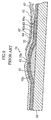
- Fig. 7 is a schematic plan view of a prior art thin-film thermal printhead.
- the thermal printhead 51 includes an elongated rectangular substrate 52 having longitudinal sides 52a and 52b.
- the substrate 52 has a surface formed with a linear resistor layer 53 extending longitudinally adjacent one longitudinal side 52a.
- a band-like region between the resistor layer 53 and the longitudinal side 52a of the substrate 52 is provided with a common wiring pattern 54.
- the common wiring pattern 54 has opposite ends extending to the other longitudinal side 52b of the substrate 52.
- One of the opposite ends of the common wiring pattern 54 is connected to a common terminal 55.
- Fig. 8 is an enlarged plan view showing a principal portion of the thermal printhead 51.
- the common wiring pattern 54 includes a plurality of comb-tooth electrodes 54a extending therefrom.
- Individual electrodes 56 have respective one end extending between two adjacent comb-tooth electrodes 54a. The other end of each individual electrode 56 extends adjacent to a drive IC 57 mounted on the substrate 52 and is connected, via a non-illustrated wire-bonding pad, to an output terminal of the drive IC 57.
- the resistor layer 53 is laid over the comb-tooth electrodes 54a and the individual electrodes 56 alternate therewith, thereby defining a heating element 53a between each two adjacent comb-tooth electrodes 54a.
- the resistor layer 53 is laid over the comb-tooth electrodes 54a and the individual electrodes 56 alternate therewith, thereby defining a heating element 53a between each two adjacent comb-tooth electrodes 54a.
- Fig. 9 is an enlarged sectional view showing a principal portion of the thermal printhead 51.
- the substrate 52 formed of an insulating material such as alumina ceramic material is provided, on a surface thereof, with a glaze layer 61 extending longitudinally at a portion adjacent to the longitudinal side 52a.
- the glaze layer 61 is formed with a resistor layer 53 in the form of a thin film for covering the glaze layer.
- Conductor layers 62a, 62b are formed on the resistor layer 53 in such a mariner as to expose the resistor layer 53 at a portion at the top of the glaze layer 61.
- the exposed portion of the resistor layer 53 serves as heating elements 53a.
- the conductor layer 62b extending rightward in Fig.
- FIG. 9 serves as the individual electrodes 56, whereas the conductor layer 62a extending leftward in Fig. 9 serves as comb-tooth electrodes 54a. Further, an anti-oxidation film 63 and a protective film 64 are formed to cover the heating elements 53a and the conductor layers 62a, 62b while exposing the wire-bonding pad of each individual electrode 56.
- An aggregate board divisible into a plurality of substrates 52 may be used for forming the glaze layer 61, the resistor layer 53, the conductor layers 62a, 62b and the anti-oxidation film 63A.
- a protective film 64 is further formed on the aggregate board thus formed with the anti-oxidation film 63.
- the protective film 64 may be formed in the following manner for example. First, a resist layer 65 is formed to cover the region, including the wire-bonding pads, which is not to be covered with the protective film 64. Then, a Ta 2 O 5 film for example may be formed by chemical vapor deposition or spattering. Subsequently, the resist layer 65 is etched away.
- the aggregate board thus formed with the protective film 64 is then divided into a plurality of individual substrates 52 to each of which drive ICs 57 are mounted.
- the drive ICs 57 and the individual electrodes 56 are connected by wire-bonding for example to provide a thermal printhead 51.
- the thermal printhead 51 is prepared by dividing the aggregate board after forming the protective film 64. Accordingly, the divisional surface 66, namely the side surface of the substrate 52 along the longitudinal side 52a at longitudinal edge of each layer 61, 53, 62a, 63, are not formed with the protective film 64. Thus, the divisional surface 66 is exposed.
- the division of the aggregate board is performed, for example, by providing a nick along a scribing line and then applying stress therealong. This results in irregularities at the divisional surface 66, which is, therefore, in poor condition. In this way, the divisional surface 66 of the thermal printhead 51 is not only in a poor condition but also is exposed.
- the edge of the substrate 52 along the longitudinal side 52a or the edges of the layers 61, 53, 62a, 63 may chip or break if the side surface of the substrate 52 along the longitudinal side 52a comes into contact with the casing or any other object.
- the protective film 64 is formed by first forming the resist layer 65 and then removing the resist layer 65 after the growth of the protective film, an edge 64a of the protective film 64 results in a step which is equivalent in height to the thickness to the protective layer 64. Then the thermal printhead 51 having such a step at the edge 64a of the protective film 64 is incorporated in an image forming apparatus, an edge of a recording paper 67 transferred in contact with the heating elements 53a may get caught at the step. In such a case, the image forming apparatus recognizes a paper jam because the recording paper 67 does not reach the heating elements 53a, thus resulting in stoppage of the apparatus.
- a thermal printhead Another method of making a thermal printhead is also proposed wherein a plurality of substrates 71 are laminated in such a manner as to expose a film-forming portion of each substrate 71 which is subsequently formed with a protective film by spattering (See e.g. JP-A-5-92596), as shown in Fig. 10.
- a plurality of projections 72 each made of the same material as the glaze layer are formed in a row on the surface of the substrate. These projections 72 are provided to prevent the laminated substrates 71 from rubbing against each other to avoid damaging of the individual electrodes or other elements due to such rubbing.
- a thermal printhead comprising: a multiplicity of heating elements formed in a row on an obverse surface of an elongated substrate at a portion which is offset widthwise toward one longitudinal side of the substrate, and a protective film formed on the obverse surface of the substrate at the widthwise offset portion for covering the heating elements, wherein the protective film is formed to extend on the obverse surface of the substrate continuously from the widthwise offset portion onto one longitudinal side surface of the substrate, and wherein a longitudinal edge of the protective film directed toward the other longitudinal side of the substrate is tapered.
- the protective film extends to a boundary between said one longitudinal side surface and a reverse surface of the substrate.
- a method of forming a thermal printhead which comprises a multiplicity of heating elements formed in a row on an obverse surface of an elongated substrate at a portion which is offset widthwise toward one longitudinal side of the substrate, and a protective film formed on the obverse surface of the substrate at the widthwise offset portion for covering the heating elements; the method comprising the steps of: forming heating elements on an aggregate board which is divisible into a plurality of substrates; dividing the aggregate board into a plurality of substrates each formed with the heating elements; and forming a protective film on each of the substrates; wherein the protective film is formed to extend on the obverse surface of the substrate continuously from the widthwise offset portion onto one longitudinal side surface of the substrate; and wherein a longitudinal edge of the protective film directed toward the other longitudinal side of the substrate is tapered.
- the protective film is formed to extend to a boundary between said one longitudinal side surface and a reverse surface of the substrate.
- the protective film is formed in a state in which the plurality of substrates are laminated in a thickness direction but shifted widthwise from each other so that portions to be formed with the protective film are exposed.
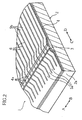
- FIG. 1 A preferred embodiment of the present invention will be described with reference to Figs. 1 through 6.
- a thin-film thermal printhead is employed.
- a thermal printhead 1 includes an elongated substrate 2 formed of an insulating material such as alumina ceramic material.
- the substrate 2 is formed, at a widthwise offset portion on an obverse surface thereof, with a glaze layer 3 extending longitudinally (i.e. in the direction of the arrow AB in Fig. 2).
- the glaze layer 3 is formed by printing and baking a glass paste material for example.
- the glaze layer has a smoothly arched cross section due to the flow of the glass component during the baking.
- a resistor layer 4 in the form of a thin film is formed to cover the glaze layer 3.
- the resistor layer 4 may be formed by CVD (chemical vapor deposition) or spattering TaSiO 2 to have a thickness of 500 to 1500 ⁇ .
- Conductor layers 5a, 5b are formed on the resistor layer 4.
- the conductor layers 5a, 5b are etched or otherwise processed to expose a predetermined portion of the resistor layer 4 over the top of the glaze layer 3.
- the exposed portion of the resistor layer 4 serves as heating elements 4a.
- a plurality of slits 6 extending widthwise of the substrate 2 (i.e. in the direction of the arrow CD in Figs. 1 and 2) are formed in the resistor layer 4 and the conductor layers 5a, 5b.
- the slits 6 may be formed, for example, by etching the resistor layer 4 and the conductor layers 5a, 5b. The provision of the slits 6 allows each of the heating elements 4a to be driven individually.
- the conductor layer 5b extending rightward from the heating elements 4a in Figs. 1 and 2 serves as individual electrodes.
- the conductor layer 6a extending leftward from the heating elements 4a in Figs. 1 and 2 serves as a common electrode.
- the heating elements 4a are covered with an anti-oxidation film 7 which is formed in a manner such as to expose wire-bonding pads of the individual electrodes.
- the anti-oxidation film 7 may be formed, for example, by depositing SiO 2 into a thickness of 3000 to 6000 ⁇ through CVD or spattering.
- a protective film 8 is formed on the anti-oxidation film 7.
- the protective film 8 extends continuously so that one longitudinal edge 8a thereof lies on a longitudinal side surface 2a of the substrate 2.
- the protective film 8 on the side surface 2a reaches the boundary between the side surface 2a and the reverse surface of the substrate 2.
- the other longitudinal edge 8b of the protective film 8 is tapered.
- the protective film 8 may be formed by depositing Ta 2 O 5 or Si 3 N 4 into a thickness of from 2 to 4 ⁇ m through CVD or spattering.
- a glaze layer 3, a resistor layer 4, conductor layers 5a, 5b and an anti-oxidation film 7 are formed on an aggregate board 15 which is divisible into a plurality of substrates 2 each formed subsequently into a thermal printhead 1.
- a protective film 8 is formed on each of the individual substrates 2, instead of the aggregate board 15, after dividing the aggregate board 15 along scribing lines 16.
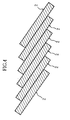
- a protective film 8 is formed on the plurality of substrates 2 simultaneously instead of forming a protective film 8 on each of the substrates 2 in a separate step.
- a protective film 8 is formed simultaneously on the respective substrates 2.
- the substrates 2 are depicted as if they are in close contact with each other. In fact, however, since the glaze layer 3 and the other layers are formed on each substrate 2, a small gap is formed between the adjacent substrates 2 when they are laminated together.
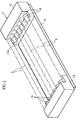
- a jig 11 shown in Fig. 5 may comprise a base member 12 and a pair of mounts 13 provided at longitudinally opposite ends of the base member 12.
- Each of the mounts 13 is formed with a plurality of retreated steps 14 (six steps in this embodiment) each extending to a side surface 13a.
- the retreated steps 14 are formed as part of a continuous serration.
- the pair of mounts 13 are disposed so that the respective serrated portions directed toward each other.
- the substrates 2 are placed so as to bridge between the retreated steps 14 of the paired mounts 13.
- a protective film 8 is formed on the exposed portion of each substrate.
- the protective film may be formed by depositing Ta 2 O 5 or Si 3 N 4 into a thickness of from 2 to 4 ⁇ m through CVD or spattering for example.
- the protective film 8 is formed not only on the anti-oxidation film 7 but also continuously onto the side surface 2a of the substrate 2.
- the spattering may be continued at least until the protective film 8 reaches the boundary between the side surface 2a and the reverse surface of the substrate 2.
- the protective film 8 covers these surface and edges. Therefore, even if the side surface 2a of the substrate 2 or the edges come into contact with a casing or any other object during handling of the thermal printhead 1 such as incorporation thereof into the casing, it is possible to prevent the side surface 2a of the substrate 2 and the edges of the layers 4, 5a, 7 from being chipped or broken.
- the portion to be formed with the protective layer 8 is exposed, whereas the portion not to be formed with such a layer is shielded by another substrate 2 laid thereon. Accordingly, it is unnecessary to form a resist layer on each substrate at a portion not to be formed with a protective layer 8, thereby eliminating the need for etching the resist layer.
- each substrate 2 laid over an adjacent substrate at a portion not to be formed with a protective film 8 is not bonded to that adjacent substrate 2. Accordingly, during the growth of the protective film 8, the edge of each substrate 2 laid over the adjacent substrate is somewhat spaced, allowing the protective film to grow at the overlapping portion. However, the film growth is slower at the overlapping portion of the substrate 2 than at the exposed portion of the substrate. As a result, the other longitudinal edge 8b of the protective film 8 is tapered to have a progressively reducing thickness toward its extremity.
- the edge 64a of the protective film 64 provides a stepped portion.
- the longitudinal edge 8b of the protective film 8 is tapered as shown in Fig. 1. Accordingly, with an image forming apparatus provided by incorporating the thermal printhead 1 in a casing or the like, the tip portion of a recording paper 21 as a recording medium is not caught at the longitudinal edge 8b of the protective film 8 during transfer of the recording paper 21. More specifically, in the image forming apparatus incorporating the thermal printhead 1, the protective film 8 is tapered at the longitudinal edge 8b to allow smooth paper transfer, as clearly shown in Fig. 1. Accordingly, a paper jam due to the provision of the protective film 8 is avoided.
- the protective film 8 is formed simultaneously on six substrates 2.
- the number of substrates 2 to which the protective film 8 is simultaneously formed may be appropriately varied.
- the design of the jig 11 for keeping the position of the substrates 2 may be modified in various ways.
- the present invention is applied to a so-called thin-film thermal printhead in the above embodiment, it is clear that the present invention may be also applied to a thick-film thermal printhead.
Landscapes
- Electronic Switches (AREA)
Abstract
Description
Claims (5)
- A thermal printhead comprising a multiplicity of heating elements formed in a row on an obverse surface of an elongated substrate at a portion which is offset widthwise toward one longitudinal side of the substrate, and a protective film formed on the obverse surface of the substrate at the widthwise offset portion for covering the heating elements,
wherein the protective film is formed to extend on the obverse surface of the substrate continuously from the widthwise offset portion onto one longitudinal side surface of the substrate, and wherein a longitudinal edge of the protective film directed toward the other longitudinal side of the substrate is tapered. - The thermal printhead according to claim 1, wherein the protective film extends to a boundary between said one longitudinal side surface and a reverse surface of the substrate.
- A method of forming a thermal printhead which comprises a multiplicity of heating elements formed in a row on an obverse surface of an elongated substrate at a portion which is offset widthwise toward one longitudinal side of the substrate, and a protective film formed on the obverse surface of the substrate at the widthwise offset portion for covering the heating elements; the method comprising the steps of:forming heating elements on an aggregate board which is divisible into a plurality of substrates; dividing the aggregate board into a plurality of substrates each formed with the heating elements; and forming a protective film on each of the substrates; wherein the protective film is formed to extend on the obverse surface of the substrate continuously from the widthwise offset portion onto one longitudinal side surface of the substrate; and wherein a longitudinal edge of the protective film directed toward the other longitudinal side of the substrate is tapered.
- The method of forming a thermal printhead according to claim 3, wherein the protective film is formed to extend to a boundary between said one longitudinal side surface and a reverse surface of the substrate.
- The method of forming a thermal printhead according to claim 3, wherein the protective film is formed in a state in which the plurality of substrates are laminated in a thickness direction but shifted widthwise from each other so that portions to be formed with the protective film are exposed.
Applications Claiming Priority (3)
| Application Number | Priority Date | Filing Date | Title |
|---|---|---|---|
| JP32423097 | 1997-11-26 | ||
| JP32423097 | 1997-11-26 | ||
| PCT/JP1998/005282 WO1999026787A1 (en) | 1997-11-26 | 1998-11-24 | Thermal print head and method of manufacturing the same |
Publications (3)
| Publication Number | Publication Date |
|---|---|
| EP1043165A1 true EP1043165A1 (en) | 2000-10-11 |
| EP1043165A4 EP1043165A4 (en) | 2001-03-07 |
| EP1043165B1 EP1043165B1 (en) | 2003-03-12 |
Family
ID=18163500
Family Applications (1)
| Application Number | Title | Priority Date | Filing Date |
|---|---|---|---|
| EP98954810A Expired - Lifetime EP1043165B1 (en) | 1997-11-26 | 1998-11-24 | Thermal print head and method of manufacturing the same |
Country Status (8)
| Country | Link |
|---|---|
| US (1) | US6304280B1 (en) |
| EP (1) | EP1043165B1 (en) |
| JP (1) | JP3996347B2 (en) |
| KR (1) | KR100339046B1 (en) |
| CN (1) | CN1108930C (en) |
| DE (1) | DE69812176T2 (en) |
| TW (1) | TW509144U (en) |
| WO (1) | WO1999026787A1 (en) |
Families Citing this family (7)
| Publication number | Priority date | Publication date | Assignee | Title |
|---|---|---|---|---|
| JP3503611B2 (en) * | 2001-04-13 | 2004-03-08 | ソニー株式会社 | Printer head, printer, and method of manufacturing printer head |
| JP4668637B2 (en) * | 2005-02-07 | 2011-04-13 | アルプス電気株式会社 | Thermal head and manufacturing method thereof |
| JP4541229B2 (en) * | 2005-05-18 | 2010-09-08 | アルプス電気株式会社 | Thermal head and manufacturing method thereof |
| JP2009137284A (en) * | 2007-11-13 | 2009-06-25 | Tdk Corp | Thermal head, manufacturing method for thermal head, and printer |
| JP5342313B2 (en) * | 2009-04-23 | 2013-11-13 | 東芝ホクト電子株式会社 | Thermal print head and manufacturing method thereof |
| JP6208607B2 (en) * | 2014-03-26 | 2017-10-04 | 京セラ株式会社 | Thermal head, thermal head manufacturing method, and thermal printer |
| JP2020151890A (en) * | 2019-03-19 | 2020-09-24 | 東芝ホクト電子株式会社 | Thermal print head and thermal printer |
Family Cites Families (12)
| Publication number | Priority date | Publication date | Assignee | Title |
|---|---|---|---|---|
| JPS606478A (en) * | 1983-06-24 | 1985-01-14 | Hitachi Ltd | thermal recording head |
| JPS6186267A (en) * | 1984-10-05 | 1986-05-01 | Toshiba Corp | Thermal head and manufacture thereof |
| JPH0661065B2 (en) | 1988-06-28 | 1994-08-10 | 三菱電機株式会社 | Cache memory control method |
| JP2546120Y2 (en) * | 1988-07-01 | 1997-08-27 | ローム株式会社 | Thermal head |
| EP0395001B1 (en) * | 1989-04-26 | 1993-12-08 | Seiko Epson Corporation | Thermal print head and method of making same |
| US5099257A (en) * | 1989-05-10 | 1992-03-24 | Matsushita Electric Industrial Co., Ltd. | Thermal head with an improved protective layer and a thermal transfer recording system using the same |
| JP2651496B2 (en) * | 1990-04-06 | 1997-09-10 | セイコー電子工業株式会社 | Thermal head |
| JP2801759B2 (en) * | 1990-09-29 | 1998-09-21 | 京セラ株式会社 | Thermal head |
| JPH0592596A (en) | 1991-09-30 | 1993-04-16 | Kyocera Corp | Manufacture of thermal head |
| US5514524A (en) * | 1993-11-22 | 1996-05-07 | Rohm Co., Ltd. | Method of making thermal printhead |
| CN1086639C (en) * | 1994-05-31 | 2002-06-26 | 罗姆股份有限公司 | Thermal printing head, substrate used thereof and method for producing the substrate |
| CN1086640C (en) * | 1994-06-21 | 2002-06-26 | 罗姆股份有限公司 | Thermal printing head, substrate used thereof and method for producing the substrate |
-
1998
- 1998-11-24 DE DE69812176T patent/DE69812176T2/en not_active Expired - Fee Related
- 1998-11-24 EP EP98954810A patent/EP1043165B1/en not_active Expired - Lifetime
- 1998-11-24 CN CN98811515A patent/CN1108930C/en not_active Expired - Lifetime
- 1998-11-24 WO PCT/JP1998/005282 patent/WO1999026787A1/en not_active Ceased
- 1998-11-24 JP JP2000521967A patent/JP3996347B2/en not_active Expired - Fee Related
- 1998-11-24 US US09/530,434 patent/US6304280B1/en not_active Expired - Lifetime
- 1998-11-24 KR KR1020007005107A patent/KR100339046B1/en not_active Expired - Fee Related
- 1998-11-26 TW TW090214716U patent/TW509144U/en not_active IP Right Cessation
Also Published As
| Publication number | Publication date |
|---|---|
| DE69812176T2 (en) | 2004-01-29 |
| US6304280B1 (en) | 2001-10-16 |
| DE69812176D1 (en) | 2003-04-17 |
| CN1108930C (en) | 2003-05-21 |
| KR20010031997A (en) | 2001-04-16 |
| KR100339046B1 (en) | 2002-06-01 |
| CN1279636A (en) | 2001-01-10 |
| EP1043165B1 (en) | 2003-03-12 |
| JP3996347B2 (en) | 2007-10-24 |
| TW509144U (en) | 2002-11-01 |
| EP1043165A4 (en) | 2001-03-07 |
| WO1999026787A1 (en) | 1999-06-03 |
Similar Documents
| Publication | Publication Date | Title |
|---|---|---|
| US6331868B1 (en) | Thermal printhead and method of making the same | |
| US6304280B1 (en) | Thermal printhead and method of making the same | |
| KR20080015837A (en) | Thermal print head | |
| US5680170A (en) | Thermal printhead | |
| EP0829369B1 (en) | Thermal head and method of manufacturing the same | |
| JPWO1999026787A1 (en) | Thermal printhead and method for manufacturing the same | |
| JP4227799B2 (en) | Thermal head and manufacturing method thereof | |
| KR100206622B1 (en) | Method of forming auxiliary electrode layer for common electrode pattern in thermal head | |
| US20070040868A1 (en) | Thermal printhead | |
| EP1077136B1 (en) | Thick-film thermal print head | |
| US7372477B2 (en) | Thermal head and manufacturing method thereof | |
| JPWO1996041722A1 (en) | Method for forming auxiliary electrode layer for common electrode pattern in thermal head | |
| US6753893B1 (en) | Thermal head and method for manufacturing the same | |
| JP3470824B2 (en) | Thermal print head | |
| EP0842783B1 (en) | Head device provided with drive ics, to which protective coating is applied, and method of forming protective coating | |
| JPH0839852A (en) | Thermal head and production thereof | |
| JP3471872B2 (en) | Thermal print head | |
| JP2657915B2 (en) | Manufacturing method of thick film thermal head | |
| JPH04163157A (en) | Thermal head | |
| KR20000071390A (en) | Thermal head and processing method thereof | |
| JPH0939282A (en) | Thermal head and manufacture thereof |
Legal Events
| Date | Code | Title | Description |
|---|---|---|---|
| PUAI | Public reference made under article 153(3) epc to a published international application that has entered the european phase |
Free format text: ORIGINAL CODE: 0009012 |
|
| 17P | Request for examination filed |
Effective date: 20000525 |
|
| AK | Designated contracting states |
Kind code of ref document: A1 Designated state(s): DE FR GB NL |
|
| A4 | Supplementary search report drawn up and despatched |
Effective date: 20010123 |
|
| AK | Designated contracting states |
Kind code of ref document: A4 Designated state(s): DE FR GB NL |
|
| 17Q | First examination report despatched |
Effective date: 20011122 |
|
| GRAH | Despatch of communication of intention to grant a patent |
Free format text: ORIGINAL CODE: EPIDOS IGRA |
|
| GRAH | Despatch of communication of intention to grant a patent |
Free format text: ORIGINAL CODE: EPIDOS IGRA |
|
| GRAA | (expected) grant |
Free format text: ORIGINAL CODE: 0009210 |
|
| AK | Designated contracting states |
Designated state(s): DE FR GB NL |
|
| PG25 | Lapsed in a contracting state [announced via postgrant information from national office to epo] |
Ref country code: NL Free format text: LAPSE BECAUSE OF FAILURE TO SUBMIT A TRANSLATION OF THE DESCRIPTION OR TO PAY THE FEE WITHIN THE PRESCRIBED TIME-LIMIT Effective date: 20030312 |
|
| REG | Reference to a national code |
Ref country code: GB Ref legal event code: FG4D |
|
| REF | Corresponds to: |
Ref document number: 69812176 Country of ref document: DE Date of ref document: 20030417 Kind code of ref document: P |
|
| NLV1 | Nl: lapsed or annulled due to failure to fulfill the requirements of art. 29p and 29m of the patents act | ||
| ET | Fr: translation filed | ||
| PLBE | No opposition filed within time limit |
Free format text: ORIGINAL CODE: 0009261 |
|
| STAA | Information on the status of an ep patent application or granted ep patent |
Free format text: STATUS: NO OPPOSITION FILED WITHIN TIME LIMIT |
|
| 26N | No opposition filed |
Effective date: 20031215 |
|
| PGFP | Annual fee paid to national office [announced via postgrant information from national office to epo] |
Ref country code: DE Payment date: 20081120 Year of fee payment: 11 |
|
| PGFP | Annual fee paid to national office [announced via postgrant information from national office to epo] |
Ref country code: GB Payment date: 20091118 Year of fee payment: 12 |
|
| PG25 | Lapsed in a contracting state [announced via postgrant information from national office to epo] |
Ref country code: DE Free format text: LAPSE BECAUSE OF NON-PAYMENT OF DUE FEES Effective date: 20100601 |
|
| GBPC | Gb: european patent ceased through non-payment of renewal fee |
Effective date: 20101124 |
|
| PG25 | Lapsed in a contracting state [announced via postgrant information from national office to epo] |
Ref country code: GB Free format text: LAPSE BECAUSE OF NON-PAYMENT OF DUE FEES Effective date: 20101124 |
|
| PGFP | Annual fee paid to national office [announced via postgrant information from national office to epo] |
Ref country code: FR Payment date: 20111118 Year of fee payment: 14 |
|
| REG | Reference to a national code |
Ref country code: FR Ref legal event code: ST Effective date: 20130731 |
|
| PG25 | Lapsed in a contracting state [announced via postgrant information from national office to epo] |
Ref country code: FR Free format text: LAPSE BECAUSE OF NON-PAYMENT OF DUE FEES Effective date: 20121130 |